The demand for carrier printed circuit boards (PCBs) is increasing in tandem with the growing complexity and miniaturization of electronic equipment and systems, as well as the need for improved signal integrity, lower power consumption, and higher data rates. Carrier PCBs serve as a stable and reliable platform for configuring and interconnecting multiple electronic components, including microprocessors, memory chips, sensors, and power devices.
The development of carrier PCBs is being driven by several key trends. Firstly, there is increasing adoption of advanced materials and fabrication methods such as HDI (high-density interconnect) and microvia technology, which allow for denser component placements and shorter signal paths. Secondly, the integration of passive and active components directly onto the PCB substrate is gaining prominence, enabling manufacturers to design more compact and efficient electronic systems.
In addition, the importance of Carrier PCB in telecommunication lies in its ability to provide a reliable platform for transmitting and receiving data at high speeds, while also managing power consumption and reducing interference. With the increasing demand for faster and more efficient communication systems, Carrier PCB has become an indispensable part of modern telecommunication technology.
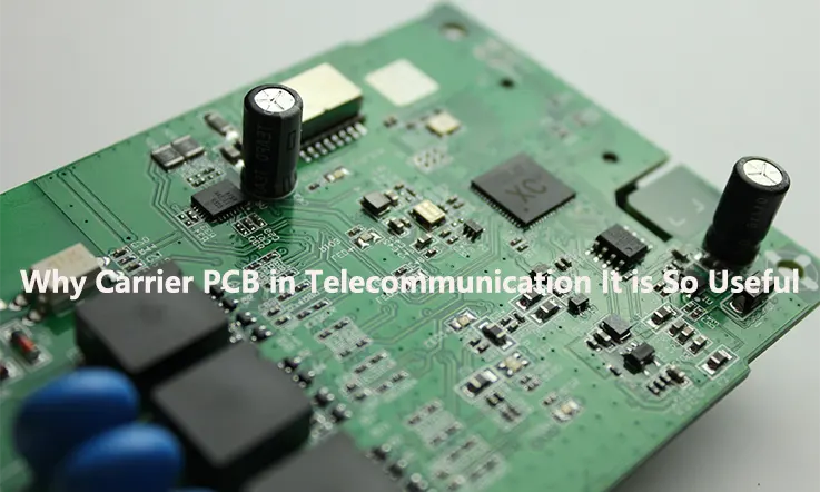
What Is Carrier PCB ?
A Carrier PCB, also known as a Printed Circuit Board, is utilized within the electronics industry to provide a solid platform with the necessary connectivity required to successfully host and integrate a diverse range of electronic components, modules, or circuit boards. This type of PCB simplifies the process of testing, prototyping, and manufacturing by offering a standard interface between the carrying PCB and the components it hosts.
Carrier PCBs can significantly improve the system’s overall reliability and maintainability by providing standardized connectivity between electronic components without requiring extensive customization or modification. Furthermore, these customized boards can be fabricated from a range of materials, such as polyimide, FR-4, or flexible materials, depending on their intended application and specific design requirements.
Advantages and Applications of Carrier PCB in Telecommunication
Carrier PCB is widely used in telecommunication systems due to its numerous advantages and applications, some of which include:
● High Speed Transmission: Carrier PCBs are designed with high-quality materials and advanced features to enable fast and reliable data transmission with reduced signal loss and attenuation.
● Enhanced Signal Integrity: Carrier PCBs are designed to reduce noise and electromagnetic interference (EMI), which helps enhance signal integrity and minimize errors in data transmission.
● Power Management: Carrier PCBs have advanced power management features that help manage power consumption and distribution in telecommunication systems, ensuring that power is utilized efficiently and effectively.
● Noise Reduction: Carrier PCBs are designed to reduce noise and interference from other circuitry and external sources, ensuring that telecommunication systems operate with minimal disruption.
● Versatility: Carrier PCBs can be used in a wide range of telecommunication applications, including cellular networks, internet routers, satellite communication systems, and more.
● Cost-Effective: Carrier PCBs offer a cost-effective solution for telecommunication systems design and manufacturing, providing high-quality performance at a relatively low cost.
How Carrier PCB Is Designed ?
Carrier PCB (Printed Circuit Board) design involves several crucial steps, including material selection, layer stackup configuration, trace routing, and component placement. Here’s a brief overview of each step:
● Material Selection: The choice of materials for Carrier PCB design is critical and depends on factors such as the frequency of operation, thermal management requirements, and cost. Materials commonly used for Carrier PCBs include FR-4, Rogers, and Isola.
● Layer Stackup Configuration: The layer stackup configuration involves determining the number and placement of copper layers in the PCB. The stackup configuration is crucial as it affects signal integrity and the routing of traces.
● Trace Routing: Trace routing involves the routing of copper traces on the PCB to connect components and carry signals. This step requires careful consideration of factors such as trace length, impedance control, and noise reduction.
● Component Placement: Component placement involves the positioning of electronic components on the PCB. Component placement affects signal integrity, thermal management, and the routing of traces on the board.
Factors to Consider for Optimal Carrier PCB Design
For optimal Carrier PCB (Printed Circuit Board) design in telecommunication systems, various factors need to be considered, including:
Signal Loss and Attenuation: Signal loss and attenuation occur when a signal travel along a trace, and its amplitude reduces due to various factors like transmission line impedance, dielectric constant, frequency, and trace routing. Good impedance control and keeping trace routing shorter can help reduce signal loss and attenuation.
Crosstalk and Electromagnetic Interference: Crosstalk and Electromagnetic Interference (EMI) are major sources of signal interference in telecommunication systems. To minimize these effects, Carrier PCB design should incorporate proper ground planes, shielding techniques, and careful trace routing.
Thermal Management: Telecommunication systems often generate significant heat due to high-speed processing and power consumption. Carrier PCB design should incorporate proper heat sinking techniques and the use of materials with high thermal conductivity to manage heat dissipation.
Board Size and Shape: The size and shape of the PCB can affect signal integrity, and board layout can substantially impact trace routing. Careful consideration should be given to board design to optimize board size and shape for efficient signal transmission.
How Does Carrier PCB Technology ?
PCB (Printed Circuit Board) technology is used in a wide range of electronic devices, including carrier PCBs. Carrier PCB technology refers to the design and manufacture of circuit boards that are used to carry or transport other electronic components, such as microprocessors, memory chips, or other integrated circuits.
A carrier PCB is essentially a support structure that provides a physical and electrical connection between the electronic components that are mounted on it. The carrier PCB typically has a number of layers, with each layer containing a network of conductive pathways that are used to connect the various components. These conductive pathways are typically made of copper, and they are etched onto the surface of the PCB using a process known as photolithography.
The process of designing and manufacturing a carrier PCB typically involves the following steps:
PCB Design: The first step in creating a carrier PCB is to design the layout of the circuit board. This involves deciding which components will be mounted on the board, and how they will be connected.
PCB Fabrication: Once the design is complete, the next step is to fabricate the PCB. This involves using a process known as photolithography to create the conductive pathways on the surface of the board.
PCB Assembly: Once the PCB has been fabricated, the next step is to assemble the electronic components onto the board. This involves placing the components onto the board and soldering them into place.
Printed Circuit Boards Testing: Finally, the carrier PCB is tested to ensure that all of the components are properly connected and functioning as intended.
Carrier PCB technology is used in a wide range of applications, including in telecommunications equipment, industrial machinery, and consumer electronics. It provides a cost-effective and reliable way to connect and transport electronic components, and it is an essential component in many electronic devices.
Real-World Applications of Carrier PCB in Telecommunication
There are various real-world applications of Carrier PCB (Printed Circuit Board) in telecommunication systems. Here are some case studies:
● Cellular Networks: Carrier PCBs are extensively used in cellular network base stations, enabling high-speed data transmission with minimal signal loss and EMI. Carrier PCBs also allow for power distribution management, which helps maximize the efficiency of cellular network systems.
● Internet Routers: Carrier PCBs play a significant role in internet routers and switches, enabling efficient and reliable data transmission across networks. For high-speed data routing, advanced Carrier PCB design techniques such as Backdrilling and Blind Via technology are used.
● Satellite Communication: Carrier PCBs are used in satellite communication systems, where high-speed and reliable data transmission is essential. The use of Carrier PCB allows for better impedance control, which helps prevent signal loss due to reflection.
● Military Communication Systems: Carrier PCBs are used in military communication systems such as satellite communication, ground systems, surveillance, and radar systems. The use of Carrier PCB allows for efficient power distribution, precise signal routing, and high-speed communication.
● Industrial Automation and Control Systems: Carrier PCBs are used in Industrial Automation and Control Systems (IACS) to provide stable, high-speed communication, and efficient power distribution. IACS often requires a higher degree of resistance to harsh environmental conditions, and Carrier PCBs with high-temperature capabilities and environmental resistance are used to address this.
Carrier PCB Networks in Phones: Their Purpose
Mobile devices rely on being connected to a network comprised of base stations and interconnections for radio equipment that enable data transmission. These essential components are owned by the carrier PCB network, including the radio spectrum utilized by serviced phones.
Telecommunications firms responsible for maintaining the network infrastructure and radio airwaves facilitate both direct service to end-users and the provision of wireless carrier services to other companies. Wireless carriers may also use other names, such as mobile phone providers or mobile service providers.
Certain mobile phone service providers may only resell the services of larger carriers and lack the necessary infrastructure. Mobile Virtual Network Operators are examples of such companies as they use the networks of established operators to provide services to their customers.
The importance of carrier network resilience is underscored by an ever-increasing demand for cellular data services. 5G-NR, the newest performance standard for cellular technology, offers faster speeds than the current 4G LTE network to wireless broadband routers and mobile devices.
Accommodating this expansion requires additional wireless spectrum and faster backbone connectivity to wireless stations. Otherwise, slow connections and network congestion will occur if capacity fails to keep up with growing demand.
Carrier PCB’s Crucial Role in the Field of Telecommunications
The internet heavily relies on data carrier circuit boards that underpin the transmission of vast amounts of data. Data often passes through numerous carrier networks before reaching the end user. Some networks may choose to waive fees for specific partners, while others may charge fees to transmit data to other networks.
● In the telecommunications industry, carrier boards play a critical role as components incorporated into the carrier system to facilitate the transmission of information, such as voice signals and video signals, through modulation of one or more high-frequency carrier signals above the primary voice frequency and data rate.
● Through multiplexing various carrier signals, a single carrier board is capable of simultaneously transmitting numerous communication channels through a shared medium. Among the different multiplexing techniques, frequency-division multiplexing and time-division multiplexing are the most common, with frequency-division multiplexing being used in cable television networks to transmit various television shows at different frequencies.
● Time-division multiplexing is utilized in public switched telephone networks to route a significant number of calls through a single trunk line. For long-distance phone conversations, frequency-division multiplexing is a viable option, allowing multiple channels to be transmitted via satellite connections. Individual channels can be demultiplexed at a particular receiving node.
Challenges and Future Directions for Carrier PCB in Telecommunication
While the use of Carrier PCB (Printed Circuit Board) has revolutionized the telecommunication industry, various challenges and future directions need to be considered, including:
High-Speed Performance: As telecommunication systems evolve to meet the ever-increasing demand for faster speed, Carrier PCB design must be optimized for high-speed performance. This requires specialized design techniques to minimize signal loss and noise while maintaining signal integrity.
● 5G Technology: The advent of 5G technology presents unique demands for Carrier PCB design, such as higher frequency operation, wider bandwidth, and increasing power consumption. As such, future Carrier PCB designs must address these challenges.
● Power Consumption: Energy efficiency is an important consideration in Carrier PCB design, as telecommunication systems consume a lot of power. Future designs must focus on minimizing power consumption and optimizing power management strategies.
● Miniaturization: The trend towards smaller and more portable telecommunication devices presents challenges for Carrier PCB design, such as the need for smaller traces, denser component packing and more complex routing.
● Cost: Despite its advantages, Carrier PCB production costs can be high, with material costs and production being a significant expense. Future Carrier PCB designs must address cost issues and seek to provide cost-effective solutions.
Therefore, addressing these challenges and focusing on future directions is essential for Carrier PCB innovation and expanding its role in telecommunication systems.
Conclusion
The carrier PCB plays a crucial role in transmitting data either via electromagnetic waves or by enabling frequency division multiplexing. Its capacity for both functions makes it an integral component in many electronic systems.
As a renowned PCB manufacturing and assembly factory in China, Janistech offers a broad range of custom PCB manufacturing services, including Medical Rigid-flex PCB, HDI PCB, Metal Core PCB, Ceramic PCB, and Carrier PCB, among others. To access our services for your upcoming PCB project, please contact us via email at [email protected]. We will respond promptly and offer expert assistance to ensure your satisfaction.
Related Posts:
1. Exceptional Manufacturer of Antenna PCBs
2. JarnisTech – High Quality Bluetooth PCB Manufacturer
3. FAQ Guide About Wireless PCB
5. What Is GPS PCB and How to Use GPS Integration into PCB?
6.The Evolution of 5G PCB Technology: Transforming the Telecommunication Industry