
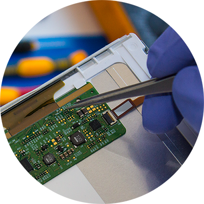
Prototype PCB assembly refers to the meticulous process of constructing printed circuit boards specifically designed for testing and validation prior to mass production. This crucial step enables designers to ensure that electronic devices perform as expected, allowing them to identify and resolve potential issues early in the development cycle. During this assembly, multiple components—such as resistors, capacitors, and integrated circuits—are precisely placed and soldered onto the PCB, forming a complete electronic circuit.
The primary objective of prototype PCB assembly is to produce a limited quantity of units that closely resemble the final product. This allows for thorough testing in real-world conditions, offering valuable insights that can guide design enhancements. For instance, a team developing a new smart thermostat might build a prototype to assess its temperature accuracy and response time under various environmental conditions. By testing this prototype, engineers can gather feedback to improve the final design, ensuring it meets both performance and quality expectations before full-scale production kicks off.
Importance in Electronics Manufacturing for Prototype PCB Assembly
Prototype PCB assembly serves an essential function in the landscape of electronics manufacturing. As devices grow in complexity, the demand for precise and reliable prototypes becomes increasingly apparent. This stage of development goes beyond mere functionality; it also addresses considerations such as manufacturability, cost efficiency, and scalability.
Investing in prototype assembly allows companies to lessen the risks associated with design flaws. For example, a smartphone manufacturer might discover during prototyping that a specific component causes interference with wireless signals. Identifying this issue at the prototype stage can save significant costs by avoiding mistakes during mass production, which could lead to delays, increased expenses, and potential harm to brand reputation.
Moreover, a well-functioning prototype fosters better communication between design and manufacturing teams. Collaboration is essential, as it ensures that the final product aligns with market demands. To illustrate, consider a startup launching a new wearable device. If the design team and assembly unit work closely together, they can streamline the process, adapting quickly to feedback and ensuring the product meets consumer expectations.
In a competitive landscape where time-to-market can greatly influence a product’s success, the responsiveness afforded by prototype PCB assembly becomes a game plan. It equips companies to swiftly adapt to shifts in consumer preferences and technological advancements, allowing them to stay ahead of the pack. Overall, leveraging prototype PCB assembly effectively can distinguish a successful product from one that struggles in the marketplace.
Key Steps in Prototype PCB Assembly
| Step | Description |
| Initial Design Review | Analyze design for manufacturability and identify potential issues. |
| Component Sourcing | Acquire high-quality components necessary for assembly. |
| PCB Fabrication | Manufacture the PCB according to design specifications. |
| Assembly | Place and solder components onto the PCB. |
| Testing | Conduct thorough tests to identify functionality and performance issues. |
| Iteration | Refine design based on testing feedback and retest as needed. |
Key Benefits of Prototype PCB Assembly
Prototype PCB assembly brings several advantages that make it a critical component of the electronics development process. Here are some of the standout benefits:
1.Cost-effective Solutions
One of the main reasons companies turn to prototype PCB assembly is its ability to save money. By detecting and addressing design flaws during the prototyping phase, organizations can sidestep the financial pitfalls that often come with mass production mistakes. For instance, consider a company designing a new handheld device. If they uncover that a particular component is prone to failure only after mass production has begun, they could face hefty expenses related to recalls, redesigns, and wasted materials.
Prototyping offers the flexibility to experiment with various components and designs without the hefty costs tied to full-scale production. This freedom allows companies to fine-tune their designs, ensuring that the final product not only meets high-quality standards but also stays within budget. For example, a manufacturer might test various resistor types in their prototype to find the one that balances performance with affordability, ultimately leading to considerable savings.
2.Quick Turnaround Times
In the competitive landscape of electronics, the ability to bring products to market swiftly can be a game changer. Prototype PCB assembly supports rapid turnaround times, enabling teams to iterate on designs efficiently. This speed is especially beneficial in markets where consumer preferences can shift quickly.
For instance, if a startup is creating a new fitness tracker, rapid prototyping allows them to test and refine their designs in a matter of weeks, rather than waiting months for a final product. This nimbleness empowers businesses to adapt based on tester feedback or emerging trends, significantly boosting their market responsiveness. By utilizing quick turnaround times, companies can roll out products that not only meet functional requirements but also resonate with current consumer interests, helping them maintain a competitive edge.
Benefits of Prototype PCB Assembly
| Benefit | Description |
| Cost-effective Solutions | Mitigates costs related to design flaws and production errors. |
| Quick Turnaround Times | Enables rapid iteration and responsiveness to market changes. |
By recognizing the key benefits of prototype PCB assembly, companies can make informed decisions that enhance their product development process. Focusing on cost-effective solutions and quick turnaround times empowers organizations to optimize their designs and better navigate the complexities of bringing innovative products to market.
Why Should You Choose JarnisTech’s PCB Assembly Prototype Services?
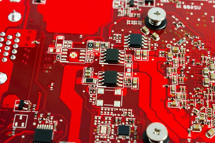 SMT&DIP Prototype PCB Assembly
1.Advantages of JarnisTech’s Services
JarnisTech’s PCB assembly prototype services come with a host of benefits that set them apart in a competitive market. With a strong focus on customer satisfaction, we provide flexible solutions that adapt to various project requirements, ensuring a seamless experience from start to finish.
2.Quality Assurance and Compliance
Quality assurance is at the forefront of JarnisTech’s PCB assembly process. We adhere to strict industry standards and best practices to ensure that every prototype meets the highest levels of performance and reliability. Rigorous testing is conducted at multiple stages of production, allowing for the identification and resolution of potential issues before the prototypes reach clients.
JarnisTech’s commitment to compliance with regulatory requirements adds another layer of trust. Whether it’s adhering to IPC standards or other relevant certifications, JarnisTech ensures that their assemblies not only function as intended but also meet all necessary safety and quality benchmarks. This attention to detail minimizes the risk of costly mistakes and enhances the overall reliability of the final product.
Quality Assurance Steps at JarnisTech
| Step | Description |
| Design Review | Analyze design for manufacturability and potential issues. |
| Component Inspection | Verify that all components meet quality standards. |
| Functional Testing | Conduct tests to ensure each prototype functions correctly. |
| Final Quality Check | Perform a comprehensive inspection before shipping. |
3.Industry Expertise
With over 20 years of experience in prototype PCB assembly, JarnisTech brings a wealth of industry knowledge to the table. Our team of skilled engineers and technicians understands the intricacies of PCB design and assembly, allowing them to provide insightful guidance throughout the project lifecycle.
This expertise enables JarnisTech to tackle a wide range of projects, from simple designs to complex assemblies. Our familiarity with the latest technologies and trends ensures that clients receive cutting-edge solutions that meet modern market demands. Moreover, this experience allows for effective problem-solving and efficient communication, fostering a collaborative environment that benefits clients.
For instance, if a client is developing a sophisticated IoT device, JarnisTech’s team can provide tailored recommendations based on their extensive experience in assembling similar products. This industry insight can significantly streamline the development process, helping clients avoid common pitfalls and achieve their project goals more efficiently.
The PCB Assembly Process
The PCB assembly process is a multifaceted operation that transforms design concepts into functional electronic devices. Understanding the stages involved is essential for achieving successful outcomes and ensuring that the final product meets both quality and performance standards. Below, we explore the key stages of PCB assembly, providing insights into each critical phase.
Stages of PCB Assembly
The PCB assembly process can be divided into several key stages, each contributing to the overall success of the project. These stages include design for manufacturability, component sourcing, fabrication, and assembly.
1.Design for Manufacturability
Design for Manufacturability (DFM) is a critical first step in the PCB assembly process. It involves optimizing the PCB design to ensure that it can be manufactured efficiently and effectively. During this stage, engineers evaluate the design for potential issues that could complicate production, such as trace widths, spacing, and component placement.
A well-executed DFM can reduce manufacturing costs and lead times by minimizing the risk of errors during assembly. For example, if a design incorporates tightly packed components, it may be difficult for automated machines to place them accurately. By addressing these concerns early, designers can create layouts that streamline production processes and enhance overall assembly efficiency.
DFM Considerations
| DFM Consideration | Description |
| Trace Widths | Ensure traces are wide enough to handle required currents. |
| Component Placement | Optimize layout to facilitate automated assembly. |
| Test Point Accessibility | Design for easy access to test points for quality assurance. |
2.Component Sourcing
Once the design has been finalized, the next step is component sourcing. This involves procuring all necessary parts, such as resistors, capacitors, integrated circuits, and connectors, from reliable suppliers. Effective component sourcing is crucial, as the quality of the components directly impacts the performance of the final product.
JarnisTech, for instance, emphasizes the importance of sourcing high-quality components that meet industry standards. We often maintain strong relationships with trusted suppliers, ensuring timely delivery and minimizing the risk of counterfeit or subpar parts. Additionally, JarnisTech’s team assesses alternative components to find the best balance of quality and cost, helping clients stay within budget while achieving their design goals.
3.Fabrication and Assembly
The fabrication and assembly stage is where the magic happens. During fabrication, the PCB is manufactured based on the finalized design, which includes etching the copper layers, drilling holes, and applying surface finishes. After the PCB is fabricated, the assembly process begins, which typically involves the following steps:
●Component Placement
●Soldering
●Inspection
●Functional Testing
Prototype Printed Circuit Board Assembly Process Steps
The prototype printed circuit board (PCB) assembly process involves several critical steps that ensure a successful transition from design to a functional prototype. By following a structured approach, teams can streamline development and improve the reliability of the final product. Below, we outline the key steps in the PCB assembly process.
Step-by-Step Guide to PCB Assembly
The PCB assembly process can be broken down into distinct phases, each essential for achieving a high-quality prototype. The main steps include initial consultation, prototyping and testing, and final assembly and quality checks.
1.Initial Consultation
The initial consultation is a foundational step where the client and assembly team discuss project requirements, objectives, and expectations. During this phase, key aspects such as design specifications, component choices, and project timelines are reviewed.
This collaborative approach ensures that everyone is on the same page and allows the assembly team to provide valuable insights based on their industry expertise. For instance, if a client is developing a wearable health monitor, the team can offer recommendations on component selection that aligns with the device’s intended use and regulatory requirements.
The initial consultation sets the stage for a successful project by clarifying objectives and ensuring that both parties understand the scope and potential challenges.
2.Prototyping and Testing
Once the consultation is complete, the next step is prototyping and testing. This phase involves creating the actual PCB based on the approved design, followed by rigorous testing to validate functionality.
Prototyping: The design is translated into a physical PCB, incorporating all specified components. This stage may involve several iterations as feedback from testing can lead to design adjustments.
Testing: After the prototype is assembled, it undergoes a series of tests to evaluate performance. These tests may include functional checks, thermal assessments, and signal integrity analysis to ensure that the prototype meets the desired specifications.
For example, if the prototype is intended for high-frequency applications, specific testing protocols can be employed to verify that signal quality remains intact. By identifying any issues during this stage, teams can refine the design and enhance overall performance.
3.Final Assembly and Quality Check
The final assembly and quality check phase is where the prototype is prepared for delivery. This stage includes several important steps to ensure that the assembled PCB meets the required standards:
Final Assembly: Any remaining components are added, and the board is prepared for final inspection. This may also include applying protective coatings or encapsulating the PCB to enhance durability.
Quality Check: A thorough quality assurance process is conducted, involving multiple inspections to verify that all components are correctly placed and soldered. Automated Optical Inspection (AOI) systems may be used to detect any defects, while manual inspections ensure that everything meets the specified standards.
Documentation: Alongside the quality check, detailed documentation is created, including test results, assembly records, and compliance certificates. This information is invaluable for clients, as it provides a comprehensive overview of the assembly process and ensures traceability.
Fully Traceable PCB Assembly Procedure
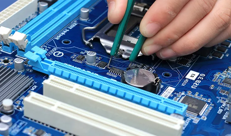 Prototype Turnkey PCB Assembly
In today’s fast-evolving electronics industry, traceability is crucial for ensuring the quality and reliability of printed circuit board (PCB) assemblies. A fully traceable PCB assembly procedure not only enhances accountability but also supports effective problem resolution and compliance with industry regulations. Below, we explore the importance of traceability in PCB assembly and how JarnisTech ensures comprehensive tracking throughout the process.
Importance of Traceability in PCB Assembly
Traceability in PCB assembly refers to the ability to track and verify every component, process, and phase involved in manufacturing and assembly. This aspect of production is beneficial for several reasons:
●Quality Assurance
●Regulatory Compliance
●Process Improvement
●Customer Confidence
Traceability Practices
| Traceability Aspect | Description | Example Impact |
| Quality Assurance | Tracking components for quality verification | Identifies defects swiftly |
| Regulatory Compliance | Meeting industry standards through documentation | Simplifies audit processes |
| Process Improvement | Analyzing data for efficiency gains | Enhances production workflows |
| Customer Confidence | Building trust through transparency | Strengthens customer relationships |
How JarnisTech Ensures Full Traceability?
JarnisTech is committed to implementing a fully traceable PCB assembly procedure, employing various strategies to ensure comprehensive tracking throughout the manufacturing process:
1.Unique Identification Codes: Each component used in the PCB assembly is assigned a unique identification code. This code is linked to detailed records, including supplier information, batch numbers, and inspection results. This system ensures that every component’s history can be easily accessed.
2.Comprehensive Documentation: JarnisTech maintains thorough documentation at every stage of the assembly process. This includes design reviews, sourcing records, assembly procedures, and quality inspection reports. All documentation is stored in a centralized database, allowing for quick access to information when needed.
3.Automated Tracking Systems: JarnisTech utilizes automated tracking systems to monitor the movement of components and assemblies throughout the manufacturing process. This real-time tracking provides visibility into each stage, ensuring that any potential issues can be addressed promptly.
4.Regular Audits and Inspections: To maintain a high level of traceability, JarnisTech conducts regular audits of their traceability processes. These audits verify that all documentation and tracking systems are functioning correctly and that traceability requirements are being met.
5.Client Access to Records: JarnisTech provides clients with access to traceability records for their assembled PCBs. This transparency enhances customer confidence and ensures that clients can verify the quality and compliance of their products.
By prioritizing traceability, JarnisTech not only enhances the quality and reliability of its PCB assemblies but also fosters trust and transparency with its clients. This commitment to traceability reflects a deep understanding of industry demands and a dedication to delivering top-notch products that meet the highest standards.
Quality Assurance in Prototype PCB Assembly
Quality assurance in prototype PCB assembly ensures that electronic devices perform reliably. Making sure each assembly meets high standards is necessary for product success. This section covers quality control, compliance with industry standards, and various testing methods used in PCB assemblies.
1.Importance of Quality Control
Quality control is a fundamental aspect of the prototype PCB assembly process. It involves a series of systematic procedures designed to identify defects, ensure consistency, and maintain high standards throughout production. The significance of quality control can be summarized in several key points:
●Reliability
●Cost Reduction
●Customer Satisfaction
●Continuous Improvement
2.Industry Standards Compliance
Compliance with industry standards is a vital component of quality assurance in prototype PCB assembly. Adhering to recognized standards not only enhances the quality of the product but also assures clients that their assemblies meet specific regulatory requirements. Some of the key standards include:
●IPC Standards
●ISO Certification
●RoHS Compliance
3.Testing Methods for Ensuring Quality
A variety of testing methods are employed in prototype PCB assembly to verify the quality and functionality of the final product. These testing methods include:
●Visual Inspection
●Automated Optical Inspection (AOI)
●Functional Testing
●In-Circuit Testing (ICT)
●Environmental Testing
How to Ask for a Prototype PCB Assembly Quote From JarnisTech?
Requesting a quote for prototype PCB assembly from JarnisTech is a straightforward process designed to facilitate effective communication and ensure that your project requirements are accurately understood. By following the outlined steps and providing the necessary information, you can receive a precise and timely quote tailored to your needs.
Steps to Request a Quote
To initiate the quoting process with JarnisTech, follow these steps:
1.Visit the Website: Start by navigating to the JarnisTech website. Here, you’ll find information about their services, capabilities, and contact details.
2.Access the Quote Request Form: Look for the dedicated quote request section or form. This is typically found under the “Services” or “Contact Us” tabs.
3.Complete the Form: Fill out the quote request form with your details. Ensure that all required fields are completed accurately to avoid any delays in processing.
4.Specify Project Details: Provide specific information about your prototype PCB assembly project, including design files and any relevant specifications. This helps the team understand your requirements better.
5.Submit the Request: After ensuring that all information is accurate and complete, submit the quote request form. You should receive a confirmation acknowledging receipt of your request.
6.Follow Up: If you don’t receive a response within the expected timeframe, consider following up via email or phone to ensure that your request is being processed.
Information Required for Accurate Quotes
To receive an accurate quote for your prototype PCB assembly, it’s essential to provide detailed information. Here’s a breakdown of the key information JarnisTech will typically require:
●Project Overview: Include a brief description of your project, including its purpose, target market, and any specific requirements that may impact the assembly process.
●Design Files: Upload the necessary design files, such as Gerber files, BOM (Bill of Materials), and schematic diagrams. These documents provide the technical specifications required for accurate quoting and assembly.
●Quantity of Prototypes: Specify the number of prototype units you need. This helps JarnisTech assess production costs and timelines.
●Component Specifications: Detail any specific components required for your project, including preferred brands or part numbers. If you have flexibility regarding component sourcing, indicate that as well.
●Assembly Type: Indicate whether you need surface mount (SMT), through-hole, or a combination of both assembly types. This information is crucial for determining the assembly process and equipment needed.
●Testing Requirements: If you require specific testing (e.g., functional testing, in-circuit testing), provide details about these requirements. This helps JarnisTech account for testing costs in the quote.
●Timeline: Share any project deadlines or timelines you have in mind. Understanding your schedule allows JarnisTech to plan accordingly and inform you of possible lead times.
●Budget Constraints: If you have a specific budget in mind, include that information. This helps the team provide options that align with your financial expectations.
Understanding PCB Assembly Costs
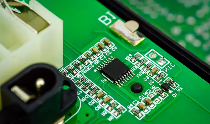 Prototype PCB Assembly
Grasping the costs associated with PCB assembly is key for effective budgeting and financial planning in electronics projects. PCB assembly costs can vary significantly due to various factors. A clear breakdown assists clients in making informed decisions.
Breakdown of PCB Assembly Costs
The costs involved in PCB assembly can be categorized into several key components, each contributing to the overall expense. Here’s a breakdown of the typical costs associated with the assembly of printed circuit boards:
●Design Costs
●Component Costs
●Manufacturing Setup Fees
●Assembly Costs
●Testing Costs
●Packaging and Shipping
●Quality Assurance and Compliance
Factors Affecting Pricing
Several factors influence the pricing of PCB assembly, and understanding these factors can help clients manage costs effectively:
●Volume of Production
●Complexity of the Design
●Component Selection
●Lead Times and Urgency
●Testing Requirements
●Geographical Location
●Quality Standards
Turnkey Solutions for Prototype PCB Assembly
Turnkey solutions in the context of prototype PCB assembly refer to comprehensive services offered by manufacturers that manage the entire process from design to delivery. These solutions are designed to simplify the development process for clients, allowing them to focus on their core competencies while ensuring that their prototypes are assembled efficiently and effectively.
What are Turnkey Solutions?
Turnkey solutions encompass all aspects of PCB assembly, including design, component sourcing, manufacturing, assembly, testing, and logistics. When a client opts for a turnkey solution, they essentially receive a “ready-to-go” product, with the assembly provider handling all the details. This approach minimizes the need for the client to coordinate with multiple suppliers and vendors, thereby reducing complexity and streamlining communication.
Advantages of Turnkey PCB Assembly
Turnkey PCB assembly offers numerous advantages that can significantly enhance the development process for businesses:
●Streamlined Manufacturing Processes
●Integrated Design Support
●Simplified Supply Chain Management
●Time and Cost Savings
Summary Table of Turnkey PCB Assembly Advantages
| Advantage | Description | Example Impact |
| Streamlined Manufacturing | Integrated workflow reduces complexity | 30% faster product launch |
| Integrated Design Support | Immediate feedback during prototyping | Improved robustness of final product |
| Simplified Supply Chain | Consolidated sourcing and manufacturing | 20% reduction in supply chain issues |
| Time and Cost Savings | Reduced overhead and faster turnaround | 15% lower production costs |
Rapid Prototyping Techniques
Rapid prototyping techniques have revolutionized the way companies develop and test new products. These methods allow for quick iterations and testing, enabling designers to validate their concepts and make necessary adjustments efficiently.
Innovations in Rapid Prototyping
Recent innovations in rapid prototyping have introduced various technologies that enhance the speed and quality of the prototyping process:
3D Printing: This technology allows for the rapid production of physical models from digital designs. 3D printing can be used to create enclosures, brackets, and other parts that accompany the PCB, providing a comprehensive view of the final product.
Additive Manufacturing: Additive manufacturing techniques enable the layering of materials to create complex geometries. This is particularly useful for designing custom components that might not be available off-the-shelf.
Advanced PCB Fabrication Techniques: Innovations such as laser-cutting and high-speed machining allow for quicker and more precise PCB fabrication. These techniques reduce turnaround times and improve the accuracy of prototypes.
Summary Table of Innovations
| Technology | Description | Example Impact |
| 3D Printing | Rapid production of physical models | Faster design iterations |
| Additive Manufacturing | Layering materials for complex geometries | Custom components for better performance |
| Advanced PCB Fabrication | Laser cutting and high-speed machining | 25% faster fabrication with improved accuracy |
Enhancing Manufacturing Efficiency
In the competitive electronics sector, boosting manufacturing efficiency is key for the success of prototype PCB assembly. By using specific strategies, companies can streamline their processes, minimize waste, and enhance productivity. Several strategies can enhance efficiency throughout the prototype assembly process:
1.Automation
Automation in PCB assembly involves using technology to perform tasks traditionally handled by people. This shift can lead to faster production times and improved consistency.
Robotic Process Automation (RPA): Incorporating robots for tasks such as component placement and soldering can significantly reduce production cycles. For instance, a manufacturer that integrated automated pick-and-place machines observed a 30% increase in speed and fewer errors.
Automated Inspection Systems: Implementing automated optical inspection (AOI) systems allows for quick identification of defects during assembly. Catching issues early helps minimize rework and scrap rates.
Example Table:
| Automation Type | Benefit | Example Impact |
| Robotic Process Automation | Increased speed | 30% faster production |
| Automated Inspection Systems | Early defect detection | Reduced rework by 25% |
2.Lean Manufacturing Principles
Lean manufacturing focuses on maximizing value while reducing waste. Applying these principles can create a more efficient assembly process.
Value Stream Mapping: This technique helps identify and eliminate non-value-added activities in the assembly process. Mapping the entire workflow can reveal bottlenecks and streamline operations.
Just-In-Time (JIT) Production: JIT practices ensure materials arrive exactly when needed, minimizing inventory costs and storage needs. A company that adopted JIT reduced its inventory holding costs by 20%, allowing for better capital utilization.
Example Table:
| Lean Principle | Benefit | Example Impact |
| Value Stream Mapping | Reduces waste | Identified bottlenecks |
| Just-In-Time Production | Lowers inventory costs | 20% less holding costs |
3.Continuous Improvement Practices
Continuous improvement, often called “Kaizen,” focuses on ongoing enhancements in processes and performance.
Employee Involvement: Encouraging team members to suggest improvements fosters a culture of innovation. Regular brainstorming sessions can lead to practical solutions that enhance efficiency.
Regular Reviews: Implementing scheduled reviews of processes helps teams identify areas for enhancement. A company that conducted quarterly reviews experienced a 15% increase in overall efficiency due to team suggestions.
Example Table:
| Continuous Improvement Practice | Benefit | Example Impact |
| Employee Involvement | Fosters innovation | New solutions for efficiency |
| Regular Reviews | Identifies improvement areas | 15% overall efficiency gain |
4.Data Analytics
Utilizing data analytics can significantly improve decision-making and operational efficiency in PCB assembly.
Real-Time Monitoring: By tracking production metrics in real time, managers can quickly spot issues and adjust processes. For instance, a manufacturer using data dashboards was able to reduce downtime by 40%.
Predictive Analytics: Employing predictive analytics helps anticipate potential equipment failures, allowing for proactive maintenance. This approach can lead to a notable reduction in unexpected downtime.
Example Table:
| Data Analytics Technique | Benefit | Example Impact |
| Real-Time Monitoring | Quick issue identification | 40% reduction in downtime |
| Predictive Analytics | Prevents equipment failures | Significant downtime reduction |
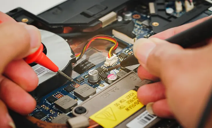 Prototype SMT PCB Assembly Test
Custom PCB Solutions
In today’s fast-evolving electronics landscape, standard solutions often fall short of meeting the unique demands of various applications. Custom PCB solutions allow companies to tailor their products specifically to their requirements, ensuring optimal performance and functionality.
Tailoring PCB Assembly to Specific Needs
Custom PCB assembly involves designing and manufacturing PCBs that cater to the distinct needs of different industries or applications. This process encompasses a variety of considerations, including size constraints, specific component requirements, and unique performance criteria.
1.Design Flexibility: Custom PCB solutions offer the flexibility to design circuits that fit specific size and shape constraints. For example, companies working on wearable technology may require smaller, lighter PCBs that conform to ergonomic designs without sacrificing functionality.
2.Component Selection: Custom assemblies allow for the selection of specialized components that enhance performance for particular applications. Whether it’s high-frequency components for telecommunications or robust materials for automotive applications, the right components can make all the difference.
3.Specialized Features: Many projects require unique features, such as custom connectors, embedded components, or specific thermal management solutions. Custom PCB assembly can integrate these features from the outset, ensuring that the final product meets all necessary specifications.
4.Prototyping for Unique Applications: In industries such as medical or aerospace, where reliability and compliance are paramount, custom prototyping allows for rigorous testing and validation of unique designs before mass production.
Case Studies of Successful Custom Projects
1.Wearable Health Devices: A health tech company approached us to develop a custom PCB for a wearable heart monitor. They required a compact design with low power consumption and integrated wireless communication capabilities. By collaborating closely with their engineering team, we designed a PCB that met all their specifications. The result was a highly efficient device that gained FDA approval and is now widely used in the market.
2.Automotive Safety Systems: Another project involved developing a custom PCB for an automotive safety system. The client needed a robust board capable of operating in high-temperature environments and meeting stringent automotive standards. We utilized high-temperature materials and implemented extensive testing protocols to ensure compliance. The custom solution enhanced the overall safety features of the vehicle and contributed to the client’s success in securing key contracts with automotive manufacturers.
3.Industrial Automation Equipment: A manufacturing company sought our expertise to create a custom PCB for their industrial automation equipment. They required a design that could interface with various sensors and actuators while also providing real-time data processing capabilities. Our engineering team developed a modular design that allowed for easy updates and scalability. This adaptability enabled the client to stay competitive in a rapidly changing market.
4.Telecommunications Infrastructure: We collaborated with a telecommunications provider to design a custom PCB for a new network device. The client needed a board that could handle high-frequency signals and support advanced communication protocols. Our team focused on optimizing signal integrity and minimizing electromagnetic interference. The resulting product improved network performance and reliability, leading to increased customer satisfaction.
Challenges in Prototype PCB Assembly
While prototype PCB assembly is an essential step in the electronics development process, it is not without its challenges. Companies often face various hurdles that can impact timelines, costs, and product quality. Understanding these common issues and their solutions is vital for successful project management.
1.Common Issues and Solutions
●Component Availability: One of the most frequent challenges in prototype assembly is sourcing components. Supply chain disruptions or long lead times can delay the assembly process.
●Solution: Establish relationships with multiple suppliers to diversify sourcing options. Using alternative components or considering local suppliers can also mitigate delays.
●Design Errors: Mistakes in the PCB design can lead to costly rework and delays during the assembly process.
●Solution: Implement rigorous design reviews and validation checks before proceeding to assembly. Using advanced design software with simulation capabilities can help identify potential errors early on.
●Testing Failures: Prototypes often fail during testing due to design flaws or assembly issues, which can lead to significant setbacks.
●Solution: Invest in thorough testing protocols, including functional and in-circuit testing, to catch issues early. Creating a robust feedback loop between testing and design teams can help refine prototypes more efficiently.
2.Lead Time Management
Effective lead time management is crucial for successful prototype PCB assembly. Delays can significantly impact product launch timelines and market competitiveness.
●Setting Realistic Timelines: Underestimating the time required for various stages of the assembly process can lead to rushed projects and subpar quality.
●Solution: Use historical data to create more accurate timelines for each phase of the assembly process. Regularly communicate with all stakeholders to ensure everyone is aligned on expectations.
●Prioritizing Tasks: In a fast-paced environment, it can be easy to lose sight of priorities, leading to inefficiencies.
●Solution: Implement project management tools to help track progress and prioritize tasks. Utilizing Gantt charts or Kanban boards can improve visibility and accountability.
●Buffer Time for Contingencies: Unexpected issues often arise during prototype assembly that can delay progress.
●Solution: Include buffer time in project schedules to accommodate potential setbacks. This practice can prevent delays in overall timelines and allow for more flexibility in addressing issues as they arise.
3.Balancing Quality and Cost
Striking the right balance between quality and cost is a perpetual challenge in PCB assembly. Companies must ensure that they do not compromise on quality while managing budget constraints.
●Cost-cutting Measures: While it may be tempting to reduce costs by opting for cheaper components or less thorough testing, these decisions can compromise the product’s quality and reliability.
●Solution: Focus on cost-effective solutions that do not sacrifice quality. For example, investing in a thorough prototype testing phase can save money in the long run by identifying issues before mass production.
●Supplier Negotiations: Working with low-cost suppliers can sometimes lead to quality issues that can adversely affect the final product.
●Solution: Evaluate suppliers based not only on cost but also on their reputation for quality and reliability. Building long-term relationships with trusted suppliers can lead to better pricing and quality assurance.
●Quality Control Practices: Implementing stringent quality control measures can increase upfront costs but is crucial for long-term success.
●Solution: Develop and adhere to a robust quality assurance framework that includes regular inspections, testing protocols, and compliance with industry standards. This proactive approach can help prevent costly recalls and rework.
Wrapping Up
If you’re ready to take your electronic product to the next level, JarnisTech is here to help. Our expert team is dedicated to providing top-notch prototype PCB assembly services tailored to your specific needs. Whether you require design support, component sourcing, or rapid prototyping, we have the solutions to ensure your project is a success.
Contact Us for Your Prototype PCB Assembly Needs
Don’t hesitate to reach out! Contact us today to discuss your prototype PCB assembly requirements. Our knowledgeable staff is eager to assist you with any questions or concerns you may have. Let us help you bring your ideas to life efficiently and effectively.
Email: [email protected]
Phone: (0755) 230-3465
Website: www.jarnistech.com
Partner with JarnisTech and experience the difference in quality and service for all your prototype PCB assembly needs!
Advanced PCB Assembly
PCBs We Can Assemble
- Min size: PCB whose width/length is less than 30mm should be panelized.
- Max size: single board 500mm*400mm | panel board 310mm*410mm.
- Layer Count: 1-60 layers (1-20 layers for mass production).
- Copper Thickness: 1/2oz – 17oz.
- PCB Types: Rigid PCBs, Flex PCBs, Rigid Flex PCBs, Rogers PCBs, Ceramic PCBs, etc.
- Surface Finishes: Lead/Lead-free HASL, ENIG, ImSilver, OSP, Gold plated, Immersion Gold, etc.
Components We Can Assemble
- SMT sizes: 01005, 0201 or larger.
- BGA pitch: 0.35mm or greater.
- BGA Ball count: 2 – 50.
- Fine pitch: 0.4mm or greater.
- WLCSP pitch: 0.35mm or greater.
- Components Height: 0.1mm – 12mm.
- BGA, micro-BGA, POP, CSP, LGA package, Flip chip, Hard metric connectors, Cable & wire, etc.
- Min. Components Spacing: 0.20mm for SMT parts, no specific demand for Thru-hole parts.
Custom PCB Assembly Capabilities
- Quick Turn.
- IPC III standard compliant.
- Prototype Quantities to Production Quantities.
- Single PCB Assembly and PCB Panel Assembly.
- Single and Double-sided PCB Assembly.
- Leaded Assembly, Lead-free or RoHS Compliant Assembly and No-clean Process Assembly.
- SMT Assembly, Thru-hole (DIP) Assembly, and Combo of SMT and Thru-hole Assembly.
- Consigned PCB Assembly, Partial consigned PCB Assembly and Full turnkey PCB Assembly.


