
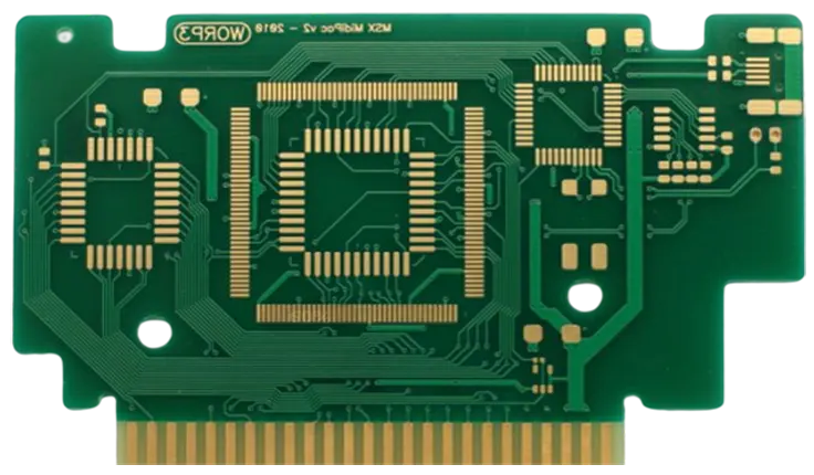
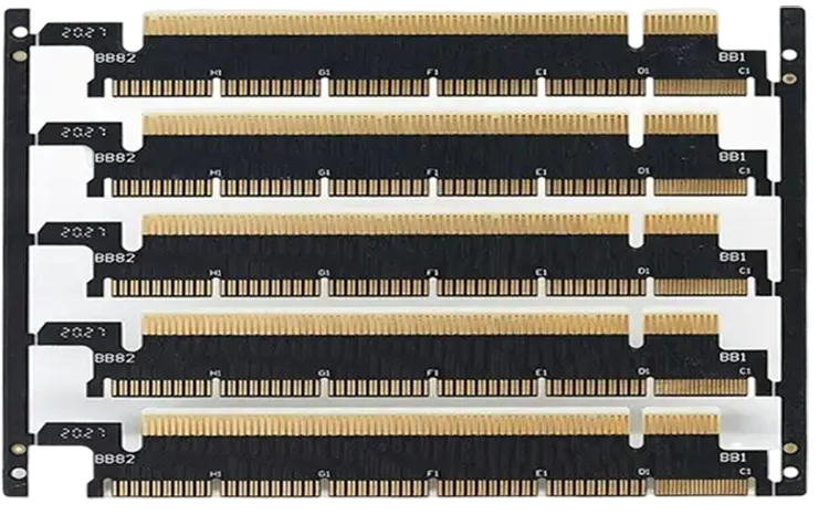
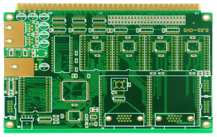
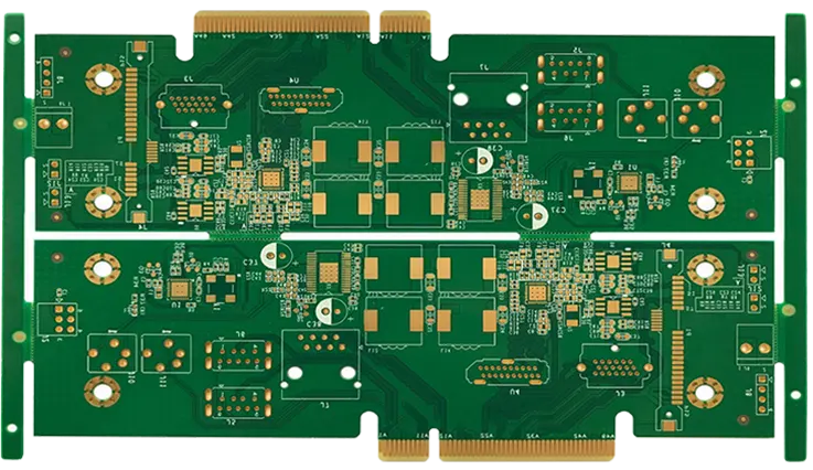
Goldfinger PCBs, known for their unique edge connectors, are a cornerstone of modern electronic design, offering unparalleled durability and seamless connectivity for high-performance applications. From their meticulous manufacturing processes to the choice of premium materials, every step is fine-tuned to meet the rigorous demands of industries such as telecommunications, automotive, and consumer electronics.
This article delves into every aspect of Goldfinger PCB production, from understanding the nuances of gold plating thickness and thermal management to the art of sourcing the right supplier. Through detailed insights, professional tips, and data-backed tables, you’ll uncover how to strike a perfect balance between cost and quality, ensuring that your Goldfinger PCBs perform flawlessly under all conditions. Whether you’re a seasoned PCB designer or new to the field, this guide equips you with the know-how to make informed decisions and optimize your PCB assembly processes. So, let’s jump into the nitty-gritty and explore what makes Goldfinger PCBs the go-to choice for precision and reliability.
Goldfinger PCB: Essential Features and Benefits
One of the defining aspects of Goldfinger PCBs is their adaptability across diverse applications. For example, they’re integral to the modular design of computer hardware, allowing components like GPUs and RAM sticks to communicate efficiently. Additionally, their design, which includes chamfered edges and precise gold-plating thickness, ensures reduced insertion wear and prolonged lifespan.
| Feature | Technical Advantage | Common Application |
| Thick Gold Plating (3-50 µin) | Minimizes resistance, ensures long-term durability | Server motherboards, routers |
| Chamfered Edge Design | Enables smooth insertion and prevents mechanical stress | Gaming consoles |
| High Corrosion Resistance | Maintains performance in high-humidity environments | Automotive electronics |
The Impact of Goldfinger PCB on Advanced Electronics
Goldfinger PCBs enable precise, low-loss signal transmission, making them indispensable for devices requiring consistent performance under demanding conditions. Imagine a high-speed data server processing terabytes of information or a gaming console handling real-time inputs without glitches—these are the scenarios where Goldfinger PCBs truly shine.
As we knon that Industrial automation systems. These setups often include modular units that need to be quickly replaced or upgraded. Goldfinger PCBs ensure robust connections while facilitating hassle-free assembly and disassembly, making them a practical choice for such dynamic environments.
Key Features of Goldfinger PCB for Longevity
The longevity of Goldfinger PCBs is directly linked to their design specifications. Here’s a deeper dive into the features that set them apart:
1.Gold Thickness and Uniformity-
The thickness of gold plating determines the board’s resistance to wear and oxidation. Typically ranging from 3 µin for consumer products to 50 µin for industrial applications, this layer ensures reliable performance even after thousands of insertion cycles.
2.Beveling and Connector Design-
Beveled edges help smooth out the insertion process by cutting down on mechanical friction, keeping both the PCB and the connector in good shape. This feature holds its ground especially in setups that see heavy action, like gaming rigs or testing gear, where wear and tear can rack up fast.
3.Custom Pin Configurations-
Manufacturers can design Goldfinger connectors to fit specific voltage or data transfer requirements. This customization enhances compatibility across devices, ensuring optimal functionality.
| Plating Specification | Primary Application | Insertion Cycles Supported |
| 3–5 µin | Consumer electronics | 1,000+ |
| 30–50 µin | Industrial automation | 10,000+ |
Industries Driving Demand for Goldfinger PCB Technology
●Consumer Electronics: From laptops to gaming consoles, Goldfinger PCBs facilitate fast data and power transmission. In gaming devices, for example, they ensure that controllers and accessories remain responsive, even during prolonged use.
●Medical Devices: Portable diagnostic tools and monitoring systems depend on Goldfinger PCBs for precise data exchange. For instance, patient monitoring devices use these boards to guarantee accurate signal interpretation under constant operation.
●Telecommunications: High-frequency signals in telecommunications systems require minimal loss. Goldfinger PCBs ensure stable signal transmission in base stations and network routers, where reliability is non-negotiable.
How to Design a High-Performance Goldfinger PCB?
Goldfinger PCB design requires precision and adherence to specific standards to ensure seamless functionality and durability. These PCBs are often used in environments demanding high reliability, such as telecommunications, gaming, and industrial automation. Therefore, Designing a Goldfinger PCB requires a precise blend of adherence to industry standards, optimization of electrical performance, and careful physical layout planning. This section delves into practical strategies, standards, and tools that engineers use to achieve high-quality results.
IPC Standards and Guidelines for Goldfinger PCB Design
Crafting a design that aligns with IPC standards lays the groundwork for quality and seamless integration. IPC-2221 acts as the blueprint for general PCB design practices, setting the tone for everything from layout considerations to material selection. On the flip side, IPC-7351 dives into the nitty-gritty of land pattern design, making sure edge connectors in Goldfinger PCBs meet the demands of precision and reliability. Following these guidelines is like having a GPS for your PCB project—keeping you on track and steering clear of costly detours.
Key considerations when following IPC guidelines include-
●Gold Plating Requirements: IPC recommends 3–50 µin plating thickness based on use cases. Industrial designs often lean toward the higher end to withstand wear from repeated insertions.
●Connector Beveling: Chamfered edges between 30° and 45° help with smooth insertion into sockets.
●Surface Finish: ENIG (Electroless Nickel Immersion Gold) is commonly used for uniform gold plating, ensuring a reliable contact area.
| Design Parameter | IPC Recommendation | Reason |
| Gold Thickness | 3–50 µin | Prevents wear and ensures conductivity |
| Bevel Angle | 30°–45° | Minimizes insertion damage |
| Connector Length | 1.0 mm minimum | Ensures stable mechanical connection |
| Clearance from Traces | ≥ 0.5 mm | Prevents accidental short circuits |
Signal Integrity Optimization in Goldfinger PCB Layouts
Keeping signal integrity on point in Goldfinger PCBs requires meticulous attention to high-speed signal design while taming signal loss, crosstalk, and EMI (electromagnetic interference). These challenges crank up the heat in fields like telecom and gaming hardware, where even a small glitch can throw the whole system out of whack. By optimizing trace impedance, deploying proper grounding techniques, and leveraging controlled dielectric materials, designers can dodge these pitfalls. Think of it as tuning a guitar—every adjustment has to be precise to hit the right chord without any distortion.
Key techniques include-
1.Differential Pair Design: For high-speed connections (e.g., PCIe), maintain consistent spacing between differential signal pairs to reduce noise.
2.Impedance Control: Use simulation tools like HyperLynx or Ansys HFSS to achieve the required impedance (e.g., 50Ω single-ended or 100Ω differential).
3.Layer Stackup Optimization: Utilize a 4-layer or 6-layer stackup with dedicated ground planes to isolate signals and reduce EMI.
| Parameter | Recommended Value | Effect on Performance |
| Differential Pair Spacing | 0.15 mm | Reduces crosstalk between signals |
| Impedance | 50Ω (single) / 100Ω (differential) | Ensures clean signal transmission |
| Layer Stackup | 4-layer / 6-layer | Enhances isolation and EMI protection |
Best Practices for Edge Connector Placement in Goldfinger PCBs
The placement of Goldfinger edge connectors directly impacts usability and reliability. Improper placement can lead to mechanical stress or alignment issues during assembly.
Key best practices include-
1.Connector Placement: Position Goldfinger connectors on the edge with the least mechanical load. For double-sided PCBs, stagger the positions to avoid alignment problems.
2.Clearance and Isolation: Maintain at least 0.5 mm clearance between Goldfinger connectors and other traces.
3.Solder Mask: Exclude solder mask from the Goldfinger area to ensure clean electrical contact during mating.
| Design Aspect | Best Practice | Impact |
| Connector Edge | Shortest PCB edge | Minimizes mechanical stress |
| Clearance | ≥ 0.5 mm | Prevents electrical interference |
| Solder Mask Removal | Over Goldfinger area only | Ensures direct and reliable contact |
How Choosing the Best Materials for Goldfinger PCB?
When you’re building a Goldfinger PCB, choosing the right materials is like picking the right tools for a job—it’s all about getting the best performance for the least amount of hassle. Each layer, each laminate, and each trace plays a part in how the board functions and holds up over time. So, let’s break down what really goes into the material selection for these advanced boards and how to make sure you’re choosing the right options for your Goldfinger PCB.
Comparing FR4 and Advanced Laminates for Goldfinger PCB
FR4 is the workhorse of the PCB world, but when it comes to Goldfinger PCBs, you’ll want to ask yourself: Is it the best choice for my application? Let’s break it down.
1.FR4 Material – The Standard Choice-
FR4 is the most common PCB laminate, made from glass-fiber and epoxy resin. It’s reliable, affordable, and performs decently under most conditions. However, for Goldfinger PCBs—especially those used in high-density and high-frequency applications—FR4 might not always be the ideal choice.
Properties:
●Dielectric Constant: Around 4.5 at 1 MHz
●Tensile Strength: Medium to High
●Thermal Conductivity: 0.3 to 0.4 W/mK
When to Use FR4: This material is a go-to when cost is a concern or when the design doesn’t require super high performance. It works fine for most consumer electronics, gaming consoles, and basic communication devices.
2.Advanced Laminates – Upgrading Performance-
When Goldfinger PCBs are tasked with managing intricate designs, high-frequency signals, or challenging environments, advanced laminates like Polyimide and PTFE (Teflon) step up to the plate. These high-performance materials excel in scenarios where maintaining signal integrity, dissipating heat efficiently, and withstanding demanding conditions are non-negotiable. Whether it’s the robust thermal stability of Polyimide or the exceptional dielectric properties of Teflon, these laminates deliver the kind of reliability and resilience that complex systems demand. It’s like upgrading to high-octane fuel for a race car—everything just performs better, even under pressure.
Properties of Advanced Laminates:
●Polyimide: High flexibility, excellent temperature stability, and low dielectric constant.
●PTFE (Teflon): Low loss factor, great for high-frequency circuits.
●Thermal Conductivity: PTFE: 0.3 W/mK, Polyimide: 0.23 W/mK
●Dielectric Constant: PTFE: ~2.0, Polyimide: ~3.0 at 1 GHz
When to Use Advanced Laminates: For cutting-edge designs, like those in aerospace, telecommunications, and high-end computing, advanced laminates should be your first choice. If you’re running at higher frequencies (5 GHz or more), these materials keep signal loss to a minimum.
Example Case Study on Material Comparison:
| Material | Thermal Conductivity (W/mK) | Dielectric Constant | Best Use Case |
| FR4 | 0.3 – 0.4 | 4.5 at 1 MHz | Standard electronics, low-to-mid frequency applications |
| Polyimide | 0.23 | ~3.0 at 1 GHz | High-frequency, flexible designs, harsh environments |
| PTFE (Teflon) | 0.3 | ~2.0 at 1 GHz | Very high-frequency circuits, aerospace, and advanced telecommunications |
Role of Copper Weight in Goldfinger PCB Performance
When it comes to Goldfinger PCBs, copper weight isn’t just a number—it’s about getting the right balance between conductivity, heat dissipation, and mechanical strength. The amount of copper used on the PCB’s layers significantly influences the board’s overall performance.
1.What is Copper Weight-
Copper weight refers to the thickness of the copper that’s used in the PCB manufacturing process. This is usually measured in ounces per square foot (oz/ft²). Common weights are 1 oz/ft² and 2 oz/ft², though you can go up to 6 oz/ft² for more demanding applications.
Effect on Performance:
●Higher Copper Weight: A higher weight typically means better current handling capabilities, better heat dissipation, and more mechanical strength. It’s perfect for power applications where high currents are involved.
●Lower Copper Weight: Ideal for circuits where space is at a premium, but still requires good signal performance without heavy power requirements.
2.Copper Weight and Signal Integrity-
●High-Current Applications: For Goldfinger PCBs used in power delivery or high-speed data, heavier copper ensures that your traces can carry more current without overheating. You can also get better impedance control by using heavier copper on signal traces.
●Thinner Copper: If you’re dealing with smaller form factors or lower currents, 1 oz/ft² copper is often enough. It’s thinner and more flexible, saving space without compromising on performance in low-power applications.
Copper Weight Comparison-
| Copper Weight (oz/ft²) | Thickness (mil) | Best Use Case | Effect on Performance |
| 1 oz/ft² | 35 μm | Standard circuits, low power | Good for most consumer products |
| 2 oz/ft² | 70 μm | Medium-power circuits | Suitable for power delivery and heat dissipation |
| 6 oz/ft² | 210 μm | High-power, heavy-duty designs | Ideal for power-heavy applications like high-end servers or telecommunications |
If you’re dealing with high-speed signals or power-hungry designs, don’t skimp on copper weight. It’s like choosing between a regular bike and a heavy-duty motorcycle—go with what’ll handle the load.”
Importance of Nickel Underlayer in Goldfinger PCB Construction
Nickel acts as the unsung workhorse in Goldfinger PCB construction, ensuring both the durability and efficiency of edge connectors. Its role as a barrier layer protects the gold plating from contaminants, preserving the board’s electrical conductivity. Beyond shielding, nickel’s structural integrity reinforces the connectors, letting them handle the repetitive action of plugging and unplugging without breaking a sweat. Think of it as the quiet backbone of the operation—always reliable, always keeping the connections steady and performance top-notch.
1.Nickel’s Role in Durability-
Nickel serves as the go-to base layer beneath gold plating in Goldfinger PCBs for a host of practical reasons. Acting as a sturdy undercoat, it provides the mechanical muscle needed to withstand constant wear and tear from edge connector use. Its natural resistance to corrosion ensures the gold layer stays intact, maintaining its conductivity over time. Think of nickel as the unshakable foundation—keeping everything in line while handling environmental stressors like humidity and oxidation.
Properties:
●Hardness: Nickel plating is harder than gold, making the edge connectors more durable and resistant to wear and tear.
●Corrosion Resistance: It provides a shield against environmental factors such as moisture or oxidation, which is crucial for long-term durability in harsh environments.
2.Nickel and Signal Integrity-
●Electroplating Compatibility: Nickel provides a smooth interface for the gold plating, which helps ensure that the gold fingers maintain high conductivity while protecting them from degradation over time.
●Gold-Nickel Interaction: The gold-plated surface ensures superior conductivity in signal paths, while the nickel provides structural support and reduces wear, making it perfect for high-frequency applications where the Goldfinger PCB will undergo regular use.
Nickel Underlayer Comparison-
| Nickel Thickness (μm) | Gold Plating (μm) | Best Use Case | Effect on Performance |
| 5 – 10 μm | 0.05 – 0.1 μm | Standard consumer electronics | Enhanced durability, good for low-medium power |
| 10 – 15 μm | 0.1 – 0.3 μm | High-frequency, industrial | Superior wear resistance, improved electrical performance |
| 15+ μm | 0.3 μm | Aerospace, military | Maximum durability, high wear resistance |
Pro Tip: “Nickel is your secret weapon. Don’t skip on this layer, especially for designs requiring frequent insertion and removal of connectors. A thicker nickel underlayer means a longer-lasting board. It’s like building a house on a rock foundation.”
Steps in Manufacturing a Quality Goldfinger PCB
Creating a reliable Goldfinger PCB is all about getting every step right—from the design phase to the final inspection. Each process must be executed with precision to ensure high performance and durability. Think of it as a recipe where every ingredient has to be measured carefully, and each stage is like the next step in a chain reaction. We’ll take a deep dive into the key stages of manufacturing, offering tips to optimize your production.
Preparing the Edge Connector for Goldfinger PCB
The preparation of the edge connector is the first step in the Goldfinger PCB process and lays the groundwork for everything that follows. This phase ensures that the connector aligns perfectly with the devices and systems it’s designed to interface with, whether those are running at high speeds or managing substantial power. Think of it as setting up the foundation of a sturdy bridge—without a solid start, the whole structure could fail. This initial setup guarantees that the Goldfinger connectors not only fit seamlessly but also perform reliably under demanding conditions.
Cleaning the Copper Base-
The process kicks off with a thorough cleaning of the copper edge connector using advanced cleaning agents or ultrasonic technology. Think of it as wiping the slate clean before you start painting; it clears up any oils, dust, or residues that could mess with the plating.
Controlling Copper Thickness-
The copper layer needs to meet strict tolerances to ensure proper conductivity. For example, industrial standards like IPC-6012D recommend copper thickness between 1 oz/ft² to 2 oz/ft² for edge connectors. A deviation here could lead to inconsistent performance, especially in high-speed communication systems.
Surface Preparation-
Before gold deposition, a conditioning treatment is applied to smooth out imperfections and create a uniform surface for better adhesion. Picture it as prepping a canvas before applying the first stroke of paint—it’s all about laying a solid foundation.
| Process Stage | Purpose | Tools Used |
| Cleaning and Preparation | Removes impurities | Ultrasonic cleaners |
| Copper Thickness Control | Ensures consistent conductivity | Thickness measurement devices |
| Surface Conditioning | Promotes even gold adhesion | Chemical baths |
Pro-Tip: Invest in a high-quality copper-thickness tester and keep an eye on IPC standards to avoid nasty surprises during quality checks. Nobody wants a customer callback over a misstep here.
Electroplating Techniques for Goldfinger PCB Production
Electroplating is where the PCB earns its “goldfinger” moniker. This step ensures the board’s edge connector will provide reliable performance over countless plug-in and plug-out cycles.
Nickel as a Barrier Layer-
Before the gold layer is applied, a nickel layer is electroplated onto the copper edge. This nickel layer acts like a buffer, stopping copper atoms from migrating into the gold over time. For heavy-duty applications, a thickness of 100–200 µin is recommended for the nickel layer.
Gold Deposition-
The gold plating can be applied via two methods: electrolytic plating for hard gold or immersion plating for ENIG (Electroless Nickel Immersion Gold). While hard gold is preferred for rugged environments, ENIG offers a more economical option for low-wear applications.
Gold Thickness-
The typical thickness of gold in a Goldfinger PCB ranges from 10 µin to 50 µin, depending on the use case. For instance, gaming devices that require frequent plug-ins may demand a thicker layer compared to a static industrial PCB.
Plating Comparison:
| Type of Gold Plating | Best For | Cost | Wear Resistance |
| Hard Gold (Electrolytic) | Gaming, heavy wear devices | $$$ | High |
| ENIG (Immersion Gold) | Consumer electronics | $$ | Moderate |
Beveling and Chamfering to Enhance Goldfinger PCB Durability
Sharpening the Edge: Beveling and chamfering the PCB edge connector not only improve its fit but also prolong its lifespan. Imagine trying to insert a blunt plug into a snug socket—it’s all friction and frustration. Proper beveling ensures smooth insertion while reducing wear and tear.
Angle Precision-
The most common beveling angles range between 30° and 45°. This depends on the connector type and application. For high-frequency connectors, a steeper angle like 45° is preferred to minimize signal reflection.
Cutting Accuracy-
Using CNC milling machines, PCB manufacturers achieve bevels with a tolerance of ±0.01 mm, ensuring the connector fits snugly without creating excess friction.
Polishing the Edges-
Once beveling is complete, the edges are polished to remove burrs and sharp surfaces. This ensures a frictionless connection and extends the connector’s lifespan.
| Beveling Aspect | Standard Value | Purpose |
| Bevel Angle | 30°–45° | Ensures smooth insertion |
| Cutting Accuracy | ±0.01 mm | Avoids misalignment with connectors |
| Polishing | Burr-free edges | Reduces insertion friction |
Pro-Tip: Think about beveling as sharpening your kitchen knife—precision matters. A poorly executed bevel will have your PCB customers asking, “What were you thinking?”
How Ensuring Consistency and Durability in Goldfinger PCB Production?
When producing Goldfinger PCBs, the consistency and durability of the final product are non-negotiable. Goldfinger connectors are used in high-reliability applications where physical wear, electrical performance, and robustness are crucial. Ensuring that each PCB meets stringent quality standards requires precision at each stage of manufacturing, from the initial design to the final testing and inspection.
One of the most important considerations in Goldfinger PCB production is the gold plating thickness and uniformity. This ensures that the connectors can withstand mechanical stress and maintain conductivity over long periods. As PCBs are used in everything from industrial equipment to consumer electronics, the durability of the edge connectors must be thoroughly tested to ensure they can endure repeated insertions and removals without degradation.
Testing for Gold Plating Thickness and Uniformity:
| Gold Plating Method | Plating Thickness (microns) | Measurement Tool | Target Application |
| Electroplating | 0.5-1.5 | X-ray Fluorescence (XRF) | High-frequency circuits |
| Hard Gold | 1-3 | XRF or Microscopy | Industrial connectors |
| Soft Gold | 0.3-0.5 | Microscopy | Consumer electronics |
Inspection Methods for Goldfinger PCB Edge Connectors
Ensuring the Goldfinger PCB connectors are free from defects is essential to guarantee the performance and reliability of the final product. There are several inspection methods employed to check the structural integrity and functionality of these connectors. These methods help manufacturers detect issues such as poor gold plating, soldering defects, or potential conductivity problems before the PCBs are shipped to customers.
| Inspection Method | Purpose | Typical Equipment Used | Accuracy Level |
| Optical Microscopy | Visual inspection of surface integrity | Optical microscopes | High (for visible defects) |
| Scanning Electron Microscopy (SEM) | Detailed analysis of microstructure | SEM machines | Extremely high (for microscopic details) |
| Electrical Continuity Test | Checking for electrical conductivity | Continuity tester (multimeter) | Very high (for operational validation) |
This table showcases the three most common inspection methods used to validate the performance of Goldfinger PCBs. Optical microscopy is great for spotting visible defects, while SEM can analyze the minute details of the edge connector. The electrical continuity test ensures that the PCB performs electrically as intended.
Standards for Insertion and Removal Cycle Durability in Goldfinger PCBs
A significant challenge in the design and production of Goldfinger PCBs is ensuring that the edge connectors are durable enough to withstand numerous insertions and removals. This is especially true for high-use environments where the connectors are regularly plugged into and removed from slots. IPC standards provide guidelines for testing the durability of connectors under these conditions, ensuring long-term functionality.
| Standard | Insertion Cycles | Removal Cycles | Test Method | Expected Outcome |
| IPC-2221 | 500-1,000 | 500-1,000 | Push-pull test machine | Durability under typical use |
| IPC-2222 | 300-800 | 300-800 | Push-pull test machine | Durability for high-end connectors |
| Industry Standard (mil) | 1,000 | 1,000 | Push-pull test machine | Long-term wear for robust designs |
This table presents the insertion and removal cycle standards defined by IPC for Goldfinger PCBs. The cycle count shows how many times the connectors can be inserted and removed without affecting their function. This is particularly necessary for devices that undergo frequent use, ensuring that the connectors stay reliable even under heavy-duty conditions. By following these standards, PCB manufacturers can ensure that manufacturing Goldfinger PCBs perform consistently, even when subjected to repeated connections and disconnections.
Thermal Management Techniques During Goldfinger PCB Assembly
Managing heat during the assembly of Goldfinger PCBs is a key aspect to ensure the product’s long-term performance. If heat isn’t handled effectively, it can cause damage to sensitive components, interfere with signal integrity, or even result in PCB failure. To prevent this, we can rely on solutions like thermal vias, heat sinks, and thermal pads to enhance heat dissipation. These techniques ensure that excess heat is directed away from critical areas, keeping the board operating efficiently under heavy demands. Proper heat management also helps maintain consistent performance, even in high-stress conditions, ensuring the PCB’s durability over time.
| Thermal Management Method | Description | Use Case | Efficiency |
| Thermal Via Plating | Involves plating vias with conductive materials to transfer heat | Used in high-power PCBs like CPUs | High |
| Heat Sinks | Attach external heat sinks to components to absorb and dissipate heat | High-power devices, military applications | Moderate to high |
| Thermal Pads | Soft pads applied between components and the PCB to help distribute heat | Consumer electronics | Moderate |
The table highlights several thermal management techniques. Thermal vias are especially effective in managing heat at the component level, while heat sinks are used for larger components. Thermal pads are a simpler solution but still effective in distributing heat.
Assembling Goldfinger PCB for Maximum Performance
Assembling Goldfinger PCBs is a high-stakes process that demands precision, technical expertise, and a deep understanding of the PCB’s unique features. It’s not just about putting components on a board—it’s about ensuring every connection and signal pathway is optimized to deliver optimal performance, especially in high-density applications where every micron counts.
Challenges in Handling High-Density Goldfinger PCBs
High-density Goldfinger PCBs are a challenge due to the complexity of their design and the need for precise handling during assembly. These PCBs typically include multiple connectors, small traces, and other intricate components that require special care.
1.Design Complexity-
●High-density Goldfinger PCBs often feature multiple layers and edge connectors packed closely together. This design necessitates highly precise alignment to avoid any short circuits or connection issues. A small misalignment can lead to catastrophic failures.
●Solution: Advanced assembly machines, such as pick-and-place machines with fine-pitch capability, must be employed. These machines use advanced vision systems to guarantee component placement accuracy, ensuring minimal deviation.
2.Space Constraints-
●The compact nature of these PCBs means there’s little room for error. Misalignments, even at the micro-level, can lead to signal degradation or short-circuits.
●Solution: Specialized handling equipment, including laser-guided placement tools, can help mitigate this issue. These tools ensure precise positioning of components within tight tolerances.
Example Case Study of High-Density PCB Assembly:
| Parameter | Standard PCB Assembly | High-Density Goldfinger PCB |
| Alignment Tolerance | ±0.05 mm | ±0.01 mm |
| Connector Pitch | 0.8 mm | 0.5 mm |
| Number of Layers | 4 Layers | 6-8 Layers |
| Assembly Time (per unit) | 30 minutes | 45 minutes |
Pro-Tip: Always go for high-tech placement systems that provide automatic alignment adjustments. It will make your high-density Goldfinger PCB assembly a breeze!
Thermal Management Techniques During Goldfinger PCB Assembly
The performance of Goldfinger PCBs heavily depends on proper thermal management during the assembly process. Excessive heat during soldering or operation can wreak havoc on edge connectors, causing signal degradation or mechanical failure.
1.Preheating the Assembly-
Preheating helps reduce thermal shock during the soldering process. For Goldfinger PCBs, maintaining a preheat temperature of 120°C to 150°C ensures the connectors don’t suffer sudden thermal expansion.
2.Wave Soldering vs. Reflow Soldering-
For high-volume production, wave soldering may be the go-to, but reflow soldering offers finer control for intricate designs. Reflow ovens with zone-based temperature profiling are recommended for achieving uniform solder joints without overheating connectors.
3.Cooling Solutions During Operation-
After putting together the Goldfinger PCB, it’s smart to think about adding heat sinks or thermal vias to manage heat when the system is in use. These methods are especially relevant for devices like gaming consoles or servers, where high data loads generate significant heat. Heat sinks act like a cooling fan, drawing the heat away from critical parts, while thermal vias channel the heat through the layers of the PCB to prevent it from affecting performance. These techniques help keep your board from overheating and ensure it keeps going strong even during heavy use.
Example Temperature Profile for Goldfinger PCBs in Reflow Ovens:
| Zone | Temperature (°C) | Time (Seconds) |
| Preheat | 120–150 | 60–90 |
| Soak | 180–210 | 30–50 |
| Reflow | 230–260 | 20–40 |
| Cooling | <100 | 30–60 |
Compatibility Testing with Assembly Equipment for Goldfinger PCBs
Once the Goldfinger PCB is assembled, it’s essential to conduct compatibility testing with assembly equipment to ensure that it can withstand real-world conditions. Here are the key testing stages:
1.Functional Testing with Edge Connectors-
●Issue: Edge connectors often suffer from poor signal integrity if the PCB’s edge is not prepared correctly during the assembly process.
●Solution: Conduct functional tests on the PCB’s edge connectors after assembly. These tests should include high-speed signal integrity checks to ensure that the connectors are operating optimally without signal loss.
2.Automated Optical Inspection (AOI)-
●Issue: Visual inspection may not catch all potential issues, especially on densely populated boards.
●Solution: Use 3D AOI systems that detect issues such as soldering defects, misalignments, or potential cracks along the edge connectors.
Test Procedure Table-
| Test Type | Purpose | Test Equipment | Key Measurement |
| Functional Test | Verify signal integrity | Oscilloscope, Signal Analyzer | Signal amplitude, reflection loss |
| AOI (Automated Optical Inspection) | Detect soldering issues and defects | 3D AOI System | Misalignment, voids, cracks |
| Mechanical Stress Test | Ensure physical durability | Vibration test setup, Thermal Chamber | Connector integrity, Flexibility |
Pro-Tip: “Always test the edge connectors under real-world conditions using high-frequency signals to simulate operational stresses. The longer the test, the better prepared your Goldfinger PCB will be!”
Balancing Cost and Quality in Goldfinger PCB Production
When it comes to manufacturing Goldfinger PCBs, finding the sweet spot between cost and quality is key to delivering a product that satisfies both budget constraints and high-performance expectations. Goldfinger PCBs are integral to electronics that require reliable edge connectors, and while manufacturers strive to keep costs low, the need for durability and signal integrity often dictates the use of premium materials and processes. Striking the right balance is both an art and a science.
In this section, we’ll dive into the factors that drive Goldfinger PCB pricing, explore how to optimize design for cost-efficiency, and understand the trade-offs that occur when choosing the plating thickness.
Factors Affecting Goldfinger PCB Pricing
The cost of producing Goldfinger PCBs is determined by various factors, including materials, manufacturing techniques, and the complexity of the design. Let’s break down some of the most impactful variables:
| Factor | Impact on Cost | Explanation |
| Material Selection | High cost for premium laminates and copper | FR4 is cost-effective, while high-performance laminates like Rogers are more expensive due to their higher thermal stability. |
| Plating Thickness | Increases with thicker gold plating | Gold plating is a substantial part of the cost. Thicker plating ensures better durability but adds to the price. |
| Design Complexity | Higher complexity increases costs | Designs with finer trace widths or high-density interconnects (HDI) require more precise processes and increase production costs. |
| Volume of Production | Larger batches reduce per-unit cost | Larger production runs typically result in economies of scale, reducing the overall cost per unit. |
| Testing and Inspection | Additional testing drives up costs | Rigorous inspection for factors like plating uniformity and signal integrity adds to the cost of production. |
Material choices, the plating process, design complexity, and the scale of production are the driving forces behind cost. Manufacturers must consider these when designing their PCBs, as they directly impact not just the quality but the price.
Cost-Efficient Design Techniques for Goldfinger PCBs
When designing Goldfinger PCBs, there are several strategies to optimize costs without sacrificing quality. These design techniques focus on reducing material waste, minimizing complex processes, and streamlining the production flow.
| Technique | Benefit | Example |
| Layer Optimization | Reduces the number of layers, minimizing costs | Using fewer layers cuts down on material costs and simplifies the manufacturing process. |
| Using Standardized Components | Lowers component cost and availability issues | Opting for standard components like common connectors can reduce costs associated with custom parts. |
| Design for Manufacturability (DFM) | Streamlines production and reduces defects | Ensuring the design is easy to manufacture minimizes defects, rework, and material waste. |
| Smart Plating Choices | Selective gold plating where needed | Only plating the areas that will undergo heavy use (such as edge connectors) reduces gold usage and cuts down costs. |
The cost-efficient design techniques in this table highlight several approaches to making Goldfinger PCBs more affordable. DFM principles play a significant role in making sure the design is easy to produce, which minimizes delays and reduces the risk of defects. Opting for standardized components and selective plating can cut down on material costs without compromising performance.
Understanding the Trade-Off Between Plating Thickness and Cost
When designing Goldfinger PCBs, one of the big decisions is how thick to make the gold plating on the connectors. Gold plating plays a key role in ensuring that electrical contacts are reliable and that the edge connectors last longer. However, the thicker the gold plating, the more it will drive up costs. This creates a balancing act for manufacturers: they have to weigh performance benefits against the added expense. Getting that balance right means knowing exactly where performance is non-negotiable and where you can afford to scale back to keep costs in check. This trade-off is part of what makes designing Goldfinger PCBs a careful balancing act between durability and budget.
| Plating Thickness | Performance Impact | Cost Impact | Best Use Case |
| Thin Plating (0.3 – 0.5 microns) | Lower durability, less wear resistance | Lower cost, suitable for low to medium-use applications | Consumer electronics, low-power devices |
| Medium Plating (0.5 – 1.0 microns) | Good balance of durability and conductivity | Moderate cost, suitable for moderate-use environments | General industrial applications |
| Thick Plating (1.0 – 3.0 microns) | High durability, excellent conductivity | Higher cost, ideal for high-stress or high-reliability applications | Military, aerospace, high-end equipment |
The table above compares different gold plating thicknesses and their respective impacts on Goldfinger PCB performance and costs. Thin plating is sufficient for lower-power applications but may not stand up to frequent use. Medium and thick plating provide better durability but at an increased cost.
How to Source the Best Goldfinger PCB Suppliers?
Choosing a reliable Goldfinger PCB supplier requires more than just a cursory glance at price tags. To ensure a robust and high-performing product, buyers must delve into the technical capabilities, certifications, and service standards of potential suppliers. By knowing what to evaluate and the right questions to ask, you can build partnerships that lead to long-term success in your projects.
Evaluating Manufacturer Capabilities for Goldfinger PCB Production
Not all PCB manufacturers are equipped to handle the precise demands of Goldfinger PCB production. The following are critical areas to assess when evaluating potential suppliers:
| Capability | Why It Matters | Indicators to Check |
| Plating Technology | Ensures consistent gold plating thickness | Look for advanced plating techniques such as selective electroplating. |
| Beveling Expertise | Affects the durability and usability of connectors | Confirm if the supplier offers precise beveling and chamfering. |
| Material Options | Impacts signal performance and reliability | Verify if the supplier can source high-quality laminates and copper weights. |
| Production Volume Flexibility | Addresses scalability for both prototyping and mass production | Ensure they can handle small and large batches efficiently. |
| Testing and Quality Assurance | Guarantees reliability and compliance | Check for automated testing systems like flying probe or X-ray inspection. |
Practical Tip: Ask for case studies or references that showcase their ability to produce Goldfinger PCBs for applications similar to yours. This is a good way to gauge their experience and expertise.
Importance of ISO and IPC Certification in Goldfinger PCB Selection
Certifications are a hallmark of quality and process reliability. For Goldfinger PCBs, two of the most critical certifications are ISO (International Organization for Standardization) and IPC (Institute for Printed Circuits).
| Certification | What It Ensures | Relevance to Goldfinger PCBs |
| ISO 9001 | Consistent quality management practices | Demonstrates a supplier’s commitment to maintaining high standards. |
| IPC-A-600 | PCB acceptability standards | Ensures the supplier adheres to industry standards for PCB quality. |
| IPC-6012 | Qualification for rigid PCBs | Relevant for applications requiring precise and reliable edge connectors. |
| RoHS Compliance | Restriction of hazardous substances | Ensures environmentally friendly production practices. |
Why Choose Us for Manufacturing Goldfinger PCBs?
At JarnisTech, we specialize in crafting Goldfinger PCBs that align with your design requirements while delivering unmatched quality and durability. Here’s a closer look at how we ensure our PCBs meet the highest standards of performance and reliability.
1.Premium Gold Plating Service
Gold plating isn’t just a feature; it’s a cornerstone of reliable Goldfinger PCBs. JarnisTech provides tailored plating solutions to suit various applications:
●Electroless Nickel Immersion Gold (ENIG): Achieving a gold thickness of up to 4µ”, this plating option ensures exceptional solderability and protection against corrosion, making it perfect for general use cases.
●Hard Gold Plating: For applications where wear resistance is non-negotiable, our hard gold plating delivers thicknesses up to 50µ”. This is ideal for high-contact scenarios such as connectors and edge fingers.
●Simply let us know your plating requirements (ranging from 2µ” to 50µ”) and the number of gold fingers your PCB design includes. We’re ready to provide a detailed and competitive quote within the hour.
| Gold Plating Type | Gold Thickness (µ”) | Application | Advantages |
| ENIG | Up to 4µ” | General-purpose, corrosion-resistant | Enhanced solderability, lower cost |
| Hard Gold Plating | Up to 50µ” | High-contact, wear-resistant areas | Superior durability, longer lifespan |
Example: A customer in telecommunications needed a multi-layer PCB with 30µ” hard gold plating for high-frequency connectors. By tailoring our services, we delivered within 5 days, reducing their downtime and improving product reliability.
2.A Variety of Goldfinger Designs
Diversity in design is key to meeting the unique demands of modern industries. JarnisTech supports:
●Standard Designs: Tried-and-tested layouts for universal compatibility.
●Segmented Goldfingers: For advanced customization in industrial or specialized applications.
●Custom-Length Goldfingers: Perfectly tailored to unconventional or proprietary connectors.
Whether your project involves single-layer, double-layer, or multi-layer PCBs, we provide ENIG, ENEPIG, or hard gold plating to maximize functionality. Each design is meticulously crafted to meet electrical performance goals and durability expectations.
| Design Type | Plating Options | Layers Supported | Common Applications |
| Standard | ENIG, ENEPIG, Hard Gold | Single, Multi-layer | Consumer electronics, telecommunications |
| Segmented | ENIG, Hard Gold | Multi-layer | Medical devices, industrial automation |
| Custom-Length | ENIG, Hard Gold | All | Proprietary systems, custom equipment |
3.Exceptional Quality Assurance
Reliability starts with quality control. At JarnisTech, we don’t leave anything to chance:
●ISO9001:2015 Certification: Our operations meet globally recognized standards for consistent quality.
●UL Certification: Ensures all our PCBs comply with stringent safety requirements.
●Comprehensive Testing: Every PCB undergoes:
1.AOI (Automated Optical Inspection): Detects minute defects with high accuracy.
2.Electronic Testing: Guarantees performance under specified electrical parameters.
| Quality Control Step | Purpose | Outcome |
| ISO9001:2015 Certification | Maintains process consistency | Reliable product performance |
| UL Certification | Compliance with safety regulations | Peace of mind for end-users |
| 100% AOI Testing | Identifies manufacturing defects early | Fewer returns and rework requests |
| Electrical Performance Testing | Verifies operational specifications | Enhanced functionality and trustworthiness |
Case Study: An aerospace client required Goldfinger PCBs with tight tolerances and consistent performance in extreme conditions. Through rigorous quality checks, we delivered PCBs that exceeded their expectations.
4.Our Manufacturing Capabilities
| Feature | Capability |
| Materials | FR4, Rogers, Isola, Ventec, Alron, Teflon Shengyi, Tuc, etc. |
| Max Layers | 1-46L |
| Min. Hole Size | 8mil/0.2mm |
| PCB Thickness/Hole Size Ratio | Maximum: 12:1 |
| Gold Thickness | Hard Gold: 2 to 50µ”; ENIG: 1 to 5µ” |
| Board Thickness | 0.2-8mm |
| Min. Trace Width | 0.08mm |
| Min. Trace Space | 0.08mm |
| Minimum Space Finger to Beveling | 0.15mm (to avoid damage to fingers) |
| Surface Finishing for Goldfinger | Hard Gold , Immersion Gold, ENEPIG, ENIG+OSP, HASL+Plating Hard Gold, ENIG+Plating Hard Gold, OSP+Plating Hard Gold, etc. |
| Solder Mask | Green, Red, Yellow, Blue, White, Black, Purple, Matte Black, Matte Green |
| Silkscreen | White, Black, Red, Purple, etc. |
| Via Process | Tenting Vias, Plugged Vias, Vias Not Covered |
| Test | Fly Probe Testing (Free) and AOI Testing |
| Build Time | 4-8 Working days |
| Lead Time | 1-2 Working days |
| Certifications | ISO 9001:2015, UL, ROHS, REACH |
| Quality Standards | IPC A-600, IPC-6010 |
Why Wait? Get Started Today
JarnisTech isn’t just another manufacturer — we’re a partner dedicated to your success. From premium plating services to unmatched design flexibility and rigorous quality control, we offer the complete package. Send us your specifications, and let’s build something exceptional together.
Contact us now for a free consultation, and receive a competitive quote within one hour! Let JarnisTech help you take your Goldfinger PCB projects to the next level.
FAQs Related to Goldfinger PCB
How does the type of gold plating (hard gold vs. ENIG) affect the longevity of Goldfinger PCBs?
Hard gold is preferred for high-contact applications due to its durability and wear resistance, while ENIG is chosen for its excellent solderability and corrosion resistance in less mechanically demanding environments.
Can Goldfinger PCBs support both digital and analog signals simultaneously?
Yes, but careful consideration must be given to layout design, including isolation techniques and signal integrity management, to prevent interference between digital and analog paths.
What are the typical cleaning methods used after Goldfinger PCB manufacturing?
Cleaning methods include ultrasonic cleaning, deionized water rinsing, and specialized solvents to remove residues that might affect connector performance or solderability.
What is the maximum current capacity for a Goldfinger PCB edge connector?
The current capacity depends on the width of the Goldfinger, the thickness of the plating, and the material’s conductivity. Typically, manufacturers can provide current rating charts based on these factors.
How do environmental factors like humidity and temperature affect the performance of Goldfinger PCBs?
High humidity or extreme temperatures can lead to oxidation and potential degradation of the gold plating. Protective measures such as conformal coatings or controlled environments are often recommended.
What is the difference between segmented and continuous Goldfingers, and where are they typically used?
Segmented Goldfingers allow for selective connection of circuits, making them ideal for modular systems, while continuous Goldfingers provide uniform connectivity for simpler applications.
Are there specific requirements for Goldfinger PCBs used in medical devices?
Yes, Goldfinger PCBs for medical devices must meet strict standards like ISO 13485 and be produced using biocompatible materials to ensure safety and reliability in sensitive applications.


