The arrangement of copper and dielectric layers in a multilayer printed circuit board, commonly known as the PCB stackup, is a foundational design discipline. This layer architecture directly governs the board’s electrical performance, signal integrity, power distribution, and manufacturability. A well-executed stackup is not merely a mechanical consideration but an engineered system that enables complex electronics to function reliably. This comprehensive guide details the principles, planning methodologies, and advanced considerations involved in creating a robust and optimized multilayer PCB stackup.
The Technical Purpose of Multilayer PCB Stackup Design
A multilayer PCB’s physical construction is an electromechanical system where the arrangement of layers defines the performance ceiling for the entire electronic assembly. A comprehensive understanding of this structure is a prerequisite for high-performance design, as the stackup dictates the behavior of the board and its circuits.
Achieving Signal Integrity (SI)
Signal integrity (SI) describes the quality of an electrical signal as it moves from a driver to a receiver. In high-speed digital systems, the stackup architecture is the primary mechanism for preventing signal degradation.
●Controlled Impedance: A well-designed stackup provides stable dielectric properties (ϵr) and layer height (H). This allows for the calculation of specific trace geometries (width and thickness) to produce a target impedance, such as 50Ω for single-ended traces or 100Ω for differential pairs. Matching the impedance across the signal path minimizes reflections that can cause ringing and reduce signal margins.
●Crosstalk Mitigation: By interleaving signal layers with solid ground or power planes, the stackup contains the electromagnetic fields around a trace. This containment drastically reduces unintended energy coupling between adjacent traces, which prevents noise and false switching. Routing adjacent signal layers with orthogonal trace directions (e.g., horizontal and vertical) further minimizes this effect.
Example Data Table – Impedance & Crosstalk Control Parameters
| Parameter | Typical Value | Unit | Notes |
| Dielectric constant (ϵr) | 4.2 | — | FR-4 material at 1 GHz |
| Dielectric height (H) | 0.18 | mm | Between signal and reference plane |
| Trace width (W) | 0.15 | mm | For 50Ω single-ended impedance |
| Trace thickness (T) | 35 | μm | Standard 1 oz copper |
| Target impedance (single-ended) | 50 | Ω | ±10% manufacturing tolerance |
| Target impedance (differential) | 100 | Ω | ±10% manufacturing tolerance |
| Crosstalk (near-end, 100 mm trace) | < 3 | % | With orthogonal routing & reference plane separation |
Establishing Power Integrity (PI)
Power integrity (PI) is the delivery of stable, low-noise voltage to all active components. The stackup is fundamental to creating a low-impedance power distribution network (PDN) that can service sharp, high-frequency current demands.
●Low-Impedance Power Distribution Network (PDN): Using solid power and ground planes placed in close proximity creates a large, distributed parallel-plate capacitor. This embedded capacitance is highly effective for supplying high-frequency transient currents, supplementing discrete capacitors and lowering the overall PDN impedance.
●Stable Voltage Referencing: Solid ground planes offer a continuous, low-inductance return path directly beneath a signal trace. This configuration minimizes the signal’s current loop area, which in turn reduces electromagnetic emissions and improves the circuit’s immunity to external noise.
Managing Electromagnetic Compatibility (EMC) & Interference (EMI)
EMC is a device’s ability to function in its electromagnetic environment without generating or being susceptible to interference. The stackup provides a direct method for controlling electromagnetic interference (EMI) at the source.
●Field Containment: By routing high-speed signals on internal layers enclosed between ground or power planes (a stripline configuration), the electromagnetic fields are largely confined within the PCB’s dielectric. This prevents the fields from radiating and interfering with other devices.
●Noise Segregation: The multilayer structure permits the physical isolation of noise-generating circuits (e.g., switch-mode power supplies) from sensitive circuits (e.g., analog amplifiers). Proper layer assignment and shielding prevent noise from coupling between these distinct areas.
Effective Thermal Management
How heat from electronic components is managed directly influences a product’s long-term reliability. The PCB itself contributes to the thermal dissipation path.
●Heat Spreading: Large, solid copper planes within the PCB act as effective heat spreaders. They draw thermal energy away from hot components and distribute it across a wider board area for dissipation into the environment through convection and radiation.
●Thermal Vias: For high-power components, thermal vias create a direct, low-resistance path for heat to travel from a component’s thermal pad to internal or bottom-side copper planes. These planes then function as internal heat sinks.
From Architecture to Assembly: Bridging Design and Manufacturing
A well-considered stackup architecture is more than a design specification; it is a blueprint for successful manufacturing and assembly. The theoretical performance of a PCB can only be realized when the design is flawlessly translated into a physical, assembled product.
●Design for Manufacturability: The choice of materials and layer thicknesses affects fabrication tolerances. A design that accounts for these manufacturing variables from the outset results in a more predictable and dependable final product.
●Assembly Process Thermal Profile: The same copper planes that manage operational heat also influence the board’s thermal behavior during the soldering process. A proper stackup helps ensure uniform heating, preventing assembly defects like component shift or poor solder joints.
●Final Performance Realization: Ultimately, the PCB stackup and the component assembly form a single, interdependent system. The precision of the assembly process—from solder paste application to component placement—is what activates the performance potential established in the design phase.
A Systematic Guide to Planning a Multilayer PCB Stackup
A structured approach to stackup design prevents costly redesigns and helps the final product achieve performance targets on the first fabrication run. This guide outlines the methodical process for developing a robust and manufacturable multilayer board.
Step 1: Define Circuit Requirements and Layer Count
The process begins with an analysis of circuit complexity. This requires identifying the number and type of signal nets, component density—especially the pin-out specifications for fine-pitch BGAs—and all required power domains. A list of signals needing controlled impedance is also compiled. This information determines the minimum layer count required for the design.
Step 2: Establish Layer Order and Function
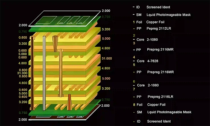
Arrange the layers in a specific sequence. A symmetrical stackup, where the layer arrangement is mirrored across the board’s centerline, should be used. This construction balances mechanical stresses during lamination and soldering, which prevents board warpage. The function of each layer (e.g., high-speed signal, ground plane, power plane) must be explicitly defined.
Step 3: Allocate Signal Layers Strategically
Signal layers should be allocated based on their performance needs. High-speed signals benefit from routing on internal layers adjacent to a solid reference plane, which provides a clean return path and good impedance control. Avoid placing two high-speed signal layers next to each other without a separating reference plane. If this arrangement is necessary, routing the traces orthogonally can help minimize crosstalk.
Step 4: Define Dielectric Materials and Thicknesses
The dielectric material and its thickness directly govern the board’s impedance characteristics and signal loss. Select appropriate materials (such as standard FR-4, high-Tg FR-4, or specialized low-loss laminates) based on the application’s operating frequency and performance requirements. The thicknesses of the core and prepreg materials are then selected to provide the specific dielectric heights (H) needed for impedance calculations.
Step 5: Specify Copper Weights
The thickness of the copper foil for each layer is specified in ounces per square foot (oz). Signal layers typically use 0.5 oz or 1 oz copper. Power and ground planes may use heavier copper (2 oz or more) to handle high currents with minimal voltage drop and to aid in thermal dissipation.
Step 6: Verify with a Field Solver and Document
Before finalization, enter the proposed stackup definition into an impedance calculator or a 2D field solver. This tool uses the specified material properties and dimensions to calculate the precise trace widths required to meet impedance targets. The final, verified stackup must be meticulously documented in a fabrication drawing, detailing every layer’s function, material type, thickness, and copper weight, along with all controlled impedance specifications.
Material Selection for Multilayer PCBs
The materials used in a multilayer PCB are active components that directly influence electrical performance, thermomechanical reliability, and overall cost. An informed material selection is a fundamental aspect of stackup engineering.
Core Dielectric and Substrate Materials
The substrate provides the PCB’s mechanical structure and primary electrical insulation between copper layers.
FR-4 (Flame Retardant 4):
This is the most prevalent substrate material, a composite of woven fiberglass cloth bonded with an epoxy resin. It is widely used due to its low cost, good mechanical properties, and mature manufacturing processes. For signals operating above a few gigahertz, however, its relatively high dissipation factor (loss tangent) can cause significant signal attenuation. Additionally, its dielectric constant can vary with frequency, which complicates precise impedance control in wideband applications.
High-Frequency Laminates:
For RF, microwave, and high-speed digital applications (e.g., >10 Gbps), specialized laminates are specified. Materials from suppliers like Rogers, Taconic, or Panasonic (e.g., Megtron series) offer substantially lower dissipation factors and more stable dielectric constants across a wide frequency range. This attribute ensures minimal signal loss and predictable impedance, which is required for high-performance channels.
Example Data Table – Substrate Material Comparison
| Property | FR-4 (Standard) | Rogers RO4350B | Panasonic Megtron 6 |
| Dielectric constant (Dk @ 1 GHz) | 4.2–4.6 | 3.48 | 3.3 |
| Dissipation factor (Df @ 1 GHz) | 0.015–0.020 | 0.0037 | 0.002 |
| Dk stability (1–10 GHz) | ±0.2 | ±0.05 | ±0.02 |
| Thermal conductivity (W/m·K) | 0.3 | 0.62 | 0.6 |
| Glass transition temperature Tg (°C) | 135–170 | 280 | 185–200 |
| Relative cost (FR-4 = 1.0) | 1.0 | 4.0 | 3.5 |
Prepreg (Pre-impregnated) Sheets
Prepreg is a thin sheet of fiberglass impregnated with partially cured (B-stage) resin. It is used to bond the layers of a multilayer board together.
Function:
During the lamination process, applied heat and pressure cause the resin in the prepreg to flow, cure, and bond the PCB layers into a single structure. The prepreg then serves as a permanent part of the dielectric insulation.
Selection:
The fabricator, in coordination with the designer, chooses the prepreg style and thickness to meet two objectives: first, to create the specific dielectric height needed for controlled impedance on adjacent layers, and second, to achieve the desired final thickness of the PCB.
Example Data Table – Common Prepreg Styles
| Prepreg Style | Glass Fabric Type | Resin Content (%) | Thickness (mm) | Typical Application |
| 106 | Very fine weave | 65 | 0.035 | Very thin dielectric spacing, high-speed SI |
| 1080 | Fine weave | 60 | 0.075 | Controlled impedance layers |
| 2116 | Medium weave | 55 | 0.105 | General-purpose bonding |
| 7628 | Coarse weave | 45 | 0.185 | Mechanical strength, thicker layers |
Copper Foil Types and Characteristics
The conductive layers are formed from copper foil, which is available in different grades that affect both manufacturability and high-speed performance.
Electrodeposited (ED) Copper:
This is the most common and cost-effective type of copper foil. It has a rough surface profile at a microscopic level, which promotes strong adhesion to the dielectric material. At very high frequencies, however, the skin effect forces signal current to flow along the conductor’s surface, and this rough profile can increase conductor losses.
Rolled-Annealed (RA) Copper:
This foil is produced by mechanically rolling a copper ingot, resulting in a much smoother surface profile. It is often selected for flexible circuits due to its superior ductility. For high-frequency rigid boards, its smoothness helps reduce conductor losses related to the skin effect, offering a performance improvement over standard ED copper.
Example Data Table – Copper Foil Comparison
| Property | ED Copper | RA Copper |
| Surface roughness (Rz, μm) | 3–5 | 1–2 |
| Conductivity (% IACS) | 100 | 100 |
| Tensile strength (MPa) | 350–400 | 300–350 |
| Elongation (%) | 5–10 | 15–20 |
| High-frequency loss impact | Higher | Lower |
| Flexibility | Poor | Excellent |
| Relative cost (ED = 1.0) | 1.0 | 1.5 |
Common Pitfalls in Multilayer Stackup Design
Awareness of common design errors is as beneficial as understanding design principles. Many well-intentioned designs are compromised by preventable oversights, and avoiding them is a mark of an experienced engineering process.
Neglecting Stackup Symmetry
This is perhaps the most frequent and consequential rule violation in multilayer design.
●The Issue: An asymmetrical stackup, where layer types, thicknesses, or copper distributions are not mirrored around the PCB’s central plane, creates unbalanced mechanical stresses. During the heat and pressure of lamination and subsequent reflow soldering cycles, these forces cause the board to warp, twist, or bow.
●The Consequence: A warped PCB creates numerous assembly problems. It can prevent proper solder paste screening, cause component misplacement by pick-and-place machines, and lead to unreliable solder joints, especially on fine-pitch components like BGAs. For all practical purposes, a non-symmetrical stackup is an unacceptable design practice.
Creating Return Path Discontinuities
High-speed signals are electromagnetic waves guided by a trace and its reference plane. Interrupting the reference path severely degrades signal integrity.
●The Issue: This error occurs when a high-speed signal transitions via to a different routing layer, but its reference plane changes without a low-inductance bridge for the return current. For example, a signal references a ground plane on Layer 2, then moves to Layer 7, which references a power plane on Layer 8. The return current must find a path from the ground plane to the power plane.
●The Consequence: Without a nearby “stitching” via connecting the two reference planes (a decoupling capacitor is ideal for this), the return current travels a long path to the nearest connection. This creates a large current loop that acts as an antenna, radiating EMI. It also introduces significant noise and timing jitter onto the signal, potentially causing channel failure.
Inadequate Power and Ground Plane Coupling
The power and ground planes are not just for DC distribution; together, they form a high-frequency capacitor that helps stabilize the entire system.
●The Issue: Some designs, particularly in lower layer counts, place the power and ground planes far apart. For instance, a 4-layer stackup of Signal | Power | Ground | Signal is a common but flawed arrangement.
●The Consequence: The capacitance of a parallel-plate structure is inversely proportional to the distance between the plates. Placing the planes far apart results in very low embedded capacitance. This increases the PDN impedance at high frequencies, reducing its ability to supply fast transient currents and making the system more susceptible to noise.
Misunderstanding Material Properties at Frequency
Treating all dielectric materials as perfect insulators with a fixed dielectric constant is an error that becomes more pronounced as signal speeds increase.
●The Issue: A designer might use the standard, low-frequency Dk value of FR-4 (e.g., ~4.5) to calculate trace impedance for a multi-gigabit signal. However, the effective Dk of FR-4 decreases as frequency increases, and its loss tangent (Df) becomes a major factor.
●The Consequence: The actual impedance of the manufactured trace will be higher than calculated, leading to reflections. Furthermore, the high Df of standard FR-4 at gigahertz frequencies will cause excessive signal attenuation (loss). The signal amplitude at the receiver may be too low to be reliably detected, causing a complete link failure. For high-speed designs, it is necessary to use material data that characterizes performance at the target frequency.
Case Study: Designing a 10-Layer Stackup for a High-Speed DDR4 Interface
This case study applies the concepts from this guide to a demanding, real-world application: a high-performance embedded board with an FPGA communicating with a DDR4 SODIMM module. This scenario requires meticulous planning for signal integrity, power integrity, and routing density.
Initial Analysis and Design Goals
The first step is to establish the specific requirements of the DDR4 interface and the overall system.
1.Performance Target: The interface will operate at a data rate of 2400 MT/s (megatransfers per second), corresponding to a 1200 MHz clock speed. This places it firmly in the high-speed design category.
2.Signal Groups: The DDR4 bus consists of several distinct signal groups, each with its own routing and impedance requirements:
●Data Group (DQ/DQS/DM): 64 data lines, 8 differential strobe pairs, and 8 data mask signals. These are point-to-point, high-speed signals requiring tight length matching within each byte lane.
●Address/Command/Control Group (ADD/CMD/CTL): These signals are routed in a multi-drop topology from the FPGA to the SODIMM.
●Clock Group (CLK): A differential clock pair, also routed in a multi-drop topology.
3.Impedance and Power Rails:
●Impedance: The JEDEC standard specifies controlled impedance: 100Ω for differential pairs (CLK, DQS) and typically 40-50Ω for single-ended signals (DQ, ADD/CMD/CTL). This design will target 40Ω for single-ended traces.
●Power: The design requires several power rails: 1.2V (VDDQ) for the I/O, 2.5V (VPP) for word line boosting, and a 0.6V termination voltage (VTT). The VDDQ and VTT rails demand very low PDN impedance.
Layer Allocation and Stackup Strategy
Based on signal density and the need for superior isolation and power integrity, a 10-layer stackup is selected. The strategy prioritizes the DDR4 signals by placing them on optimal layers.
●L1 (Top): Component placement (FPGA). Low-speed signals.
●L2 (Ground): Solid ground plane. Provides a reference for L1 and shields L3.
●L3 (Signal): High-speed DDR4 Data Group (e.g., DQ bytes 0-3). Routing as 40Ω microstrip referenced to L2.
●L4 (Signal): High-speed DDR4 Data Group (e.g., DQ bytes 4-7). Routing as 40Ω microstrip referenced to L5.
●L5 (Ground): Solid ground plane. Shields L4 and L6, providing isolation and a reference.
●L6 (Signal): DDR4 Address/Command/Control and Clock signals. Routing as stripline between L5 and L7.
●L7 (Power): 1.2V VDDQ power plane. This is placed tightly against L8 to create a high-capacitance plane pair.
●L8 (Ground): Solid ground plane. Shields L9 and provides the primary reference for the VDDQ plane.
●L9 (Signal): Non-critical signals, other power routing.
●L10 (Bottom): Component placement (SODIMM connector, decoupling caps). Other signals.
This proposed stackup places the noisiest, highest-speed signals (DQ/DQS) on layers referenced to solid ground. It isolates the data groups from the address/command group and creates a tightly coupled power-ground plane pair (L7/L8) for high-frequency decoupling. The symmetrical placement of signal and plane layers helps ensure mechanical stability.
Implementation and Verification
With the stackup defined, the next steps involve implementation and simulation to verify the design choices.
●Material Choice: A high-performance, low-loss dielectric material like Megtron 6 or Isola I-Speed is chosen over standard FR-4. This is a requirement to minimize dielectric losses at 1.2 GHz and ensure a stable Dk for accurate impedance control.
●Impedance Calculation: Using a field solver and the material properties of the chosen laminate, precise trace widths are calculated. For example, on layer L3, with a specific dielectric height to L2, a trace width of ~4.5 mils might be required to achieve 40Ω.
●PDN Analysis: A Power Integrity simulation is run, focusing on the impedance of the 1.2V VDDQ rail. The analysis confirms that the combination of the L7/L8 plane capacitance and discrete decoupling capacitors meets the target impedance required by the FPGA and DDR4 memory.
●Signal Integrity Simulation: Post-layout simulation of the DQ/DQS signals is performed. Eye diagrams are generated to confirm that the signal eye is wide open at the receiver, indicating sufficient timing and voltage margin after accounting for all channel losses and reflections.
Example Data Table – Implementation & Simulation Results
| Parameter | Value | Unit | Notes |
| Material (Laminate) | Megtron 6 | — | Dk ~ 3.4 @ 1 GHz, low-loss |
| Dielectric height (L3–L2) | 0.18 | mm | For 40Ω microstrip |
| Trace width (L3) | 4.5 | mils | Matches 40Ω target |
| PDN impedance (VDDQ @ 100 MHz) | 22 | mΩ | Below 25 mΩ requirement |
| Eye height (DQ @ RX) | 420 | mV | Meets JEDEC margin |
| Eye width (DQ @ RX) | 0.42 | UI | Passes SI requirement |
Design for Manufacturability and Assembly (DFM & DFA)
A theoretically perfect stackup has no practical value if it cannot be reliably fabricated and assembled. Considering Design for Manufacturability (DFM) and Design for Assembly (DFA) from the outset is a mark of a mature design process, bridging the gap between a schematic and a functional, high-yield product.
DFM: Ensuring High-Yield Fabrication
DFM aims to adapt the design to match the manufacturing capabilities of the PCB fabrication facility, ensuring the board can be produced with high yield and dependable performance.
●Material Availability: Before finalizing a stackup, it is wise to consult with the fabricator to confirm that the specified dielectric materials and thicknesses are standard, in-stock items. Requesting non-standard materials can result in significant cost increases and long lead times.
●Symmetry and Balance: A symmetrical layer stackup, where the layer order and thicknesses are mirrored around the board’s central plane, is a fundamental practice to prevent warpage during lamination and reflow soldering. Furthermore, the distribution of copper on each layer should be as balanced as possible to prevent localized internal stresses.
●Drilling and Aspect Ratio: The ratio of the board’s total thickness to the diameter of the smallest drilled hole is known as the aspect ratio. Every fabricator has a maximum achievable aspect ratio, beyond which the reliability of plating copper inside the via barrel is compromised. The stackup design must respect this constraint.
DFA: How Stackup Influences Assembly
DFA considers how the PCB design, including the stackup, will affect the automated process of soldering components to the board.
●Thermal Profile Management: The number and thickness of copper planes in a stackup determine the board’s overall thermal mass. A board with many heavy copper planes requires a more aggressive thermal profile during reflow soldering to ensure all solder joints reach a liquidus state. The stackup design directly informs the development of this profile.
●Component Placement and Warpage: As noted, an asymmetrical stackup is a primary cause of board warpage during the high temperatures of reflow. A warped board can cause numerous assembly defects, from poor solder paste screening to component shifting, all of which lead to poor solder joint quality.
●Via-in-Pad and Solderability: The practice of placing vias directly in component solder pads (Via-in-Pad) is common in high-density designs. However, an open via can wick solder away from the joint during reflow, leading to a weak or open connection. A proper DFA process includes instructions in the fabrication notes to have these vias filled and plated over, presenting a flat, reliable surface for soldering.
Frequently Asked Questions (FAQ)
1.How can I optimize a multilayer PCB stackup for cost-effectiveness?
●Use standard FR-4 materials, not high-frequency laminates.
●Minimize the layer count to only what is necessary.
●Keep the design symmetrical to improve manufacturing yield.
●Avoid advanced features (e.g., blind/buried vias) unless required for density.
2.Why is a symmetrical multilayer PCB stackup necessary?
A symmetrical stackup is necessary for mechanical stability. It balances stress during production to prevent board warpage that disrupts component assembly and harms long-term reliability.
3.For high-speed signals, what is a primary consideration in a multilayer PCB stackup?
The main consideration is providing a continuous return path. This is done by routing a high-speed trace adjacent to a solid reference plane (like ground) to control impedance and reduce EMI.
4.How does material selection directly impact a multilayer PCB stackup?
●Performance: Use standard FR-4 for lower-frequency signals and low-loss laminates for high-frequency signals to prevent signal degradation.
●Cost: High-performance materials are significantly more expensive, creating a direct trade-off with the product budget.
5.In a multilayer PCB stackup, what is the ideal arrangement for power integrity (PI)?
For best power integrity, place the main power and ground planes as close together as possible. This creates an embedded, low-inductance capacitor that effectively supplies the high-frequency current demanded by modern ICs.
Future Outlook: Trends in Multilayer PCB Technology
The relentless drive for smaller, faster, and more powerful electronic devices is pushing the boundaries of conventional PCB technology. The stackup of tomorrow will incorporate new materials, structures, and design methodologies to meet these future demands. Understanding these emerging trends is fundamental to remaining at the forefront of electronic design.
Embedded Components
The practice of embedding passive (resistors, capacitors) and even active components within the internal layers of a PCB is gaining traction. By fabricating these components directly into the stackup, designers can:
●Achieve significant miniaturization by increasing component density.
●Improve electrical performance by shortening connection paths.
●Enhance reliability by protecting components from environmental factors.
This approach requires a much closer collaboration between circuit design and stackup planning, as the physical layers themselves become functional circuit elements.
AI-Assisted Optimization
Designing an optimal stackup involves navigating a complex problem with trade-offs between cost, signal integrity, and manufacturability. Artificial intelligence and machine learning are being applied to this challenge.
●Future EDA tools are expected to feature AI that can explore thousands of possible stackup configurations, material choices, and layer assignments in minutes.
●This allows the system to present a set of Pareto-optimal solutions that would be impossible for a designer to find through manual iteration.
Optical Interconnects
As data rates push beyond 100 Gbps per channel, traditional copper traces face fundamental physical limits due to signal attenuation. The integration of optical waveguides directly into the PCB stackup represents a new direction.
●These thin, polymer-based channels guide light signals, offering near-zero loss, immense bandwidth, and complete immunity to electromagnetic interference.
●Designing a hybrid electro-optical stackup, which seamlessly integrates both copper and optical layers, will be a defining opportunity for the next generation of ultra-high-speed systems.
While these technologies represent the future, they all share a common requirement: a deeper, more collaborative relationship between design and production. As a partner committed to innovation, we are actively engaged in developing the processes and expertise necessary to bring these next-generation designs to life.
Selecting a Partner for Your Multilayer PCB Manufacturing
A superior multilayer PCB design requires an equally capable manufacturing partner to translate its potential into a reliable, high-performance physical product. The choice of a manufacturer has a direct bearing on the final quality, cost, and time-to-market. The following pillars define a top-tier manufacturing experience.
Uncompromising Quality and Reliability
Quality in multilayer PCB fabrication is a baseline requirement. It is achieved through disciplined adherence to industry standards and rigorous process control. This includes strict compliance with IPC-A-600 Class 2 or Class 3 standards, comprehensive Automated Optical Inspection (AOI) on every layer, and X-ray verification to ensure perfect layer-to-layer registration and via integrity. A commitment to quality is also reflected in the sourcing of traceable, high-grade raw materials, ensuring that the foundation of your board is sound.
Competitive and Transparent Value
The best value is a combination of fair pricing and high first-pass yield, preventing costly redesigns. A transparent pricing model, which provides clear, itemized quotes without hidden fees, is a mark of a trustworthy partner. Furthermore, proactive Design for Manufacturability (DFM) feedback, offered before production begins, helps identify and correct potential issues that could increase cost or compromise quality, delivering a superior product at an optimized price point.
Punctual Delivery and Proactive Communication
In today’s highly competitive market, delivering on schedule is a fundamental requirement for success. A dependable manufacturing partner runs on an efficient, well-organized production process and a comprehensive project management system, ensuring that every stage—from order placement to final shipment—is carefully optimized for swift progress. Proactive communication, including real-time progress updates and a responsive technical support team, offers transparency and reassurance throughout the entire journey.
Dedicated Engineering Support
Exceptional service transcends simple order fulfillment. It involves a collaborative partnership. Access to experienced engineers who can review designs, provide DFM/DFA feedback, and offer expert advice on material selection or stackup optimization adds immense value. Having a dedicated technical point of contact for each project ensures that complex requirements are fully understood and that any challenges are swiftly and effectively resolved.
Advanced Manufacturing Capabilities
The ability to handle complex, high-technology designs is a direct reflection of a manufacturer’s investment in advanced equipment and process expertise. Indicators of a high-capability facility include:
●Experience with high layer counts (e.g., 20+ layers).
●Proficiency with a wide range of advanced materials, including Rogers, Taconic, Isola, and Megtron.
●Advanced HDI capabilities, including sequential lamination, stacked microvias, and via-in-pad processing.
●The ability to achieve fine line widths and spacing (e.g., 3/3 mils).
●A comprehensive offering of surface finishes to meet diverse assembly and environmental requirements.
Our services
Multilayer PCB Manufacturing & Assembly