
The 10 Layer PCB is not just another multi-layer board; it’s a robust solution for modern electronic systems that require both high-speed performance and high-density functionality. 10 Layer PCBs provide more space for routing traces, enabling us to place components closer together, thus increasing circuit density and reducing overall board size. This makes 10 Layer PCBs perfect for devices that demand both complex routing and minimal footprint, such as wearables, smartphones, and medical instruments.
In this comprehensive guide, we’ll delve into the complexities of 10 Layer PCBs, exploring everything from their basic principles to advanced design techniques, and why they are increasingly sought after for a variety of high-tech industries. We’ll break down the design process, manufacturing challenges, and optimization strategies that ensure a reliable and high-performance PCB, while addressing the unique needs of industries like medical devices, 5G telecommunications, and automotive electronics.
What is a 10 Layer PCB and Why is it Necessary for High-Performance Electronics?
A 10 Layer PCB is a sophisticated type of printed circuit board (PCB) made up of ten individual layers of conductive materials, insulating layers, and vias. This design is built to address the growing demand for high-speed performance and high-density interconnections in complex and compact devices. Industries such as medical electronics, consumer electronics, and industrial equipment manufacturing rely on 10 Layer PCBs to manage high-frequency signals, minimize power loss, and ensure that end products function reliably.
Looking into the construction of a 10 Layer PCB, you’ll find that its multi-layer structure supports precise signal routing, optimized grounding, and effective heat dissipation—factors necessary for ensuring the reliability of modern electronics.
Key Features and Advantages of 10 Layer PCBs
One notable feature of 10 Layer PCBs is their capacity to maintain signal integrity. By offering dedicated layers for signal traces and grounding, the design helps ensure that signals are transmitted accurately. In high-frequency applications, this precision is needed for reliable performance.
Another factor in PCB design is electromagnetic interference (EMI), which can disrupt signal clarity. With additional layers, a 10 Layer PCB provides better shielding between inner signal layers, reducing the risk of interference. This shielding allows devices to perform with more consistency, particularly in environments where stable operation is a necessity.
How 10 Layer PCBs Enable High-Density Interconnections?
The demand for high-density interconnections (HDI) continues to rise, particularly in the consumer electronics market. Devices are becoming smaller, yet they need to offer more functions. This trend requires intricate designs that fit more components into smaller spaces.
10 Layer PCBs address this by providing the necessary space to route additional signal traces without expanding the size of the board. This multi-layer approach allows for more components to be connected without sacrificing functionality. As a result, products can be made smaller while increasing the number of capabilities.
The stack-up of a 10 Layer PCB also supports the use of fine-pitch components, which further increases the density of connections. In addition, these layers contribute to heat dissipation, ensuring that the board remains effective in high-density environments where heat management is a core consideration.
The Contribution of 10 Layer PCBs in Miniaturization and Complex Designs
As electronics become more sophisticated, the demand for miniaturization in device design is on the rise. 10 Layer PCBs offer a solution by making it possible to create smaller devices that still contain multiple components and interconnections. The ability to reduce the size of a PCB while retaining its full functionality has become a factor in the development of wearables, 5G devices, and medical equipment.
These applications require compact form factors while maintaining operational performance. A 10 Layer PCB achieves this by allowing more routing layers, making room for more components within the same limited space. Furthermore, high-speed signals can be routed with greater efficiency, and power distribution can be handled more effectively to support the various functions of the device.
Therefore, with 10 Layer PCBs, high-frequency applications can be integrated into compact devices, ensuring that performance is maintained even within limited space.
Key Design Considerations for 10 Layer PCB
Designing 10 Layer PCBs requires attention to several factors that directly affect the board’s ability to perform well in high-speed applications. When creating a 10 Layer PCB, the aim is to balance functionality and complexity to meet the needs of your electronic systems. So, considering the following points during the design process will ensure optimal results.
The design choices made during the 10 Layer PCB process influence signal integrity and impedance control. These factors help avoid problems like signal degradation, crosstalk, and noise. It’s must to carefully consider these aspects to ensure the board performs consistently in demanding environments. Let’s dive into some design factors and explore ways to achieve high performance.
Designing Effective Stack-Ups for 10 Layer PCBs
The stack-up in 10 Layer PCBs plays a central role in determining the board’s behavior. Proper stack-up design ensures that signals are routed efficiently while minimizing problems like interference and cross-talk. Effective stack-up design helps achieve impedance control, contributing to the overall signal integrity of the final board.
A well-designed stack-up includes a sequence of signal layers interspersed with power and ground planes. For instance, positioning signal layers near ground planes helps to minimize the possibility of signal distortion. This arrangement is particularly useful when trying to reduce electromagnetic interference (EMI), as the grounding layers offer a shield to prevent unwanted signals from disturbing the sensitive circuits.
Here’s a basic example of what a 10 Layer PCB stack-up might look like:
Layer 1: Signal (Top Layer)
Layer 2: Ground Plane
Layer 3: Signal
Layer 4: Power Plane
Layer 5: Signal
Layer 6: Ground Plane
Layer 7: Signal
Layer 8: Power Plane
Layer 9: Signal
Layer 10: Ground Plane (Bottom Layer)
By organizing the stack-up in this manner, we can control electrical noise, signal integrity, and heat distribution. This approach ensures stable operations for devices in complex systems.
Standard 10 Layer PCB Stack–Up-
For designers of printed circuit boards, utilizing a 10-layer stack-up is a popular and practical choice. A standard stack-up of 10 layers serves as a common option applicable in most PCB designs.
This configuration of a 10-layer stack-up confers benefits in design versatility, signal integrity, and power distribution. It’s crafted to meet a broad spectrum of design needs and is compatible with a myriad of applications.
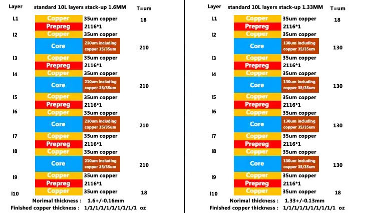
Standard 10L Stacks Up 1.6MM Standard 10L stacks up 1.33MM
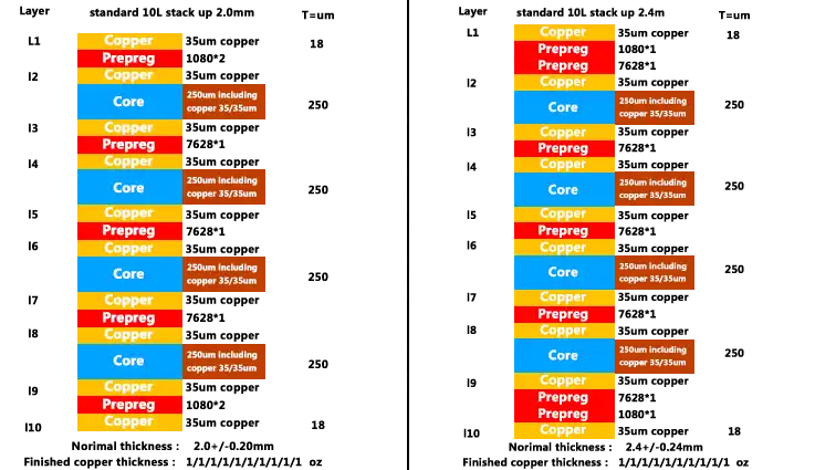
Standard 10L Stacks Up to 2.0MM Standard 10L Stacks Up 2.4MM
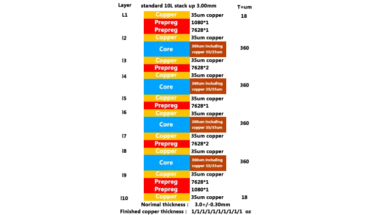
Standard 10L Stacks Up To 3.00mm
Managing High-Speed Signals in 10 Layer PCB Designs
In 10 Layer PCB designs, high-speed signal transmission is a factor to consider. As data transmission speeds increase, it’s necessary to ensure that signals travel efficiently without introducing noise or degradation. Using strategies like differential pairs helps manage high-speed signals effectively.
When designing differential pairs, two traces carry opposite signals to each other. This setup minimizes signal loss and reflections by maintaining a balanced flow of information. Additionally, it helps with the overall signal integrity throughout the board.
In high-speed designs, maintaining a consistent impedance across traces is also important to ensure that signals are transmitted without distortion. By calculating trace widths and spacing accurately, we can avoid impedance mismatch, which could lead to issues such as signal delay and errors in transmission.
Ensuring that differential pairs are properly matched and trace widths are designed according to impedance requirements guarantees smooth transmission of high-speed signals across the 10 Layer PCB.
Power and Ground Planes in 10 Layer PCB Designs
In 10 Layer PCBs, both power planes and ground planes help to ensure the stability of the entire design. The power plane serves to distribute power evenly across the board, while the ground plane maintains the reference level for signals, preventing voltage fluctuations and electrical noise from affecting performance.
Carefully positioning the power and ground planes within the 10-layer PCB stack-up can significantly reduce the chances of voltage spikes and signal interference. The ground plane helps maintain low impedance paths, ensuring that the signals stay clean and clear, especially in high-speed designs. On the other hand, the power plane provides an efficient pathway for delivering power, minimizing unwanted noise between the signal layers. This thoughtful layout results in more stable performance and a more reliable PCB overall.
The strategic placement of decoupling capacitors also plays a role in power distribution. These capacitors are placed near power pins to help manage any fluctuations in the power supply and improve overall signal performance. By ensuring a steady and reliable power source, these capacitors help the 10 Layer PCB maintain stable performance, which is especially beneficial in high-performance electronic systems.
Material Selection for High-Performance 10 Layer PCBs
When designing 10 Layer PCBs for high-speed, high-density applications, the material selection process is a consider factor in achieving optimal performance. The materials chosen directly impact the signal integrity, thermal stability, and overall durability of the board. Selecting the right materials can be the difference between a successful design and a failing one, especially in demanding industries such as medical electronics and consumer devices.
10 Layer PCBs are subject to rigorous demands from both electrical and mechanical perspectives. From high-frequency signals to temperature stability, the material selection must align with the needs of the device it serves. Let’s dive into the considerations for choosing the right material and understand how advanced materials can enhance performance while controlling costs.
Choosing the Right Material for 10 Layer PCBs
The selection of materials for 10 Layer PCBs starts with laminates and substrates that meet the specific electrical and mechanical needs of the application. High-frequency laminates are essential when working with fast signal processing and need to handle data speeds beyond standard PCB requirements. For applications that demand low-loss and high-speed signal transmission, PTFE (Polytetrafluoroethylene) based materials or ceramic-filled laminates are highly recommended. These materials are designed to offer low dielectric constant values, which help reduce signal loss and maintain signal quality.
In contrast, FR4 is one of the most commonly used laminate materials due to its cost-effectiveness and satisfactory electrical properties for general-purpose applications. However, for 10 Layer PCBs dealing with high-speed digital circuits or RF signals, specialized laminates are a must.
Here are some material choices that you should consider:
●PTFE-based laminates: Excellent for high-speed digital circuits.
●Ceramic-based materials: High-frequency, low-loss materials suitable for RF designs.
●FR4 (Standard): The go-to material for a wide range of general-purpose applications.
●Polyimide: Excellent for flexible PCBs where high-temperature resistance is necessary.
These material options support better thermal management, reducing the risks of overheating, which can lead to signal degradation or even circuit failure. For high-speed 10 Layer PCBs, selecting the right laminate material ensures that electrical signals are efficiently transmitted without distortion, even at high frequencies.
Advanced Materials for Medical and Industrial 10 Layer PCBs
Medical devices and industrial electronics operate in demanding environments where durability and reliability are non-negotiable. These applications require materials that can endure extreme temperatures, humidity, and mechanical stress, while consistently performing as expected. When designing 10 Layer PCBs for such devices, selecting high-reliability materials ensures long-term stability and meets the strict regulatory standards necessary for compliance.
For medical PCB designs, it’s essential to use materials that meet biocompatibility and safety standards. Polyimide and Teflon-based materials are frequently selected for their ability to maintain thermal stability in high-temperature settings. This characteristic is particularly useful for medical devices like diagnostic equipment and wearable health monitors, where performance in demanding conditions is a requirement.
In the case of industrial electronics, high-temperature laminates such as ceramic or high-Tg FR4 (which has a high glass transition temperature) are chosen for their resilience in harsh conditions. These materials perform reliably in industrial machinery, automotive electronics, and power systems, where environmental stress can be extreme.
Advanced materials not only ensure the performance of 10 Layer PCBs but also help meet industry standards for electromagnetic compatibility (EMC) and safety regulations. This is particularly necessary in applications such as medical devices and automotive systems, where reliability under demanding conditions is a requirement.
The Impact of PCB Materials on Performance and Cost in 10 Layer PCBs
In any 10 Layer PCB design, balancing performance and cost is a consideration. High-performance materials, while necessary in many cases, come at a higher cost.
High-performance materials like PTFE or ceramics can dramatically improve signal integrity, thermal management, and reliability, but they also come with a higher price tag. On the other hand, FR4 remains the most economical option, but it may not meet the requirements for designs involving high-frequency signals or harsh environmental conditions.
Let’s take a look at the material choices for different applications and how these choices impact performance and cost:
| Material | Advantages | Applications | Cost |
| FR4 | Affordable, easy to source, good for general use | Consumer electronics, low-speed circuits | Low |
| PTFE | Low loss, high-frequency, thermally stable | RF, high-speed digital circuits | High |
| Polyimide | High-temperature resistance, flexible | Wearables, medical devices, flex PCBs | Moderate to High |
| Ceramic | High-performance, low-loss at high frequencies | RF circuits, military, aerospace | Very High |
Choosing affordable materials like FR4 may seem like the best option for budget-conscious projects, but it could lead to performance issues in certain applications. For high-speed, high-frequency systems, using PTFE or ceramic laminates would justify the higher cost by providing better signal quality and thermal management.
On the flip side, a balanced approach that combines high-performance materials for critical layers and standard materials for less demanding layers can help optimize both cost-efficiency and performance in 10 Layer PCBs.
Understanding 10 Layer PCB Manufacturing Process
Manufacturing a 10-layer PCB requires careful planning and specialized equipment. From the design stage through to assembly, every step plays a part in making sure the board meets the demands of high-speed electronics. As high-density interconnects continue to gain traction, understanding the process of 10-layer PCB fabrication and what ensures its reliability and efficiency is must.
In this section, we’ll dive into each phase of the 10 Layer PCB manufacturing process, starting with the design and layer stacking all the way through etching, drilling, and final assembly. With multiple layers packed into a compact space, managing precision and signal integrity is key for getting the most out of these designs. Ready to break it down? Let’s get started.
Step-by-Step Guide to 10 Layer PCB Fabrication
The 10 Layer PCB fabrication process is multifaceted, involving several steps to ensure that the final product can handle high-speed signals, high-density interconnections, and thermal dissipation. Each step must be performed with precision, as even the slightest misalignment or error can affect the board’s performance. Here’s how it’s done:
1.Design and Layer Stacking: The process begins with designing the PCB layout. During this phase, our PCB designer decides the number of layers, the arrangement of signal, power, and ground layers, and other details such as trace width and impedance control. Once the design is complete, the layers are stacked in a specific order based on the signal integrity requirements.
2.Photo-Plotting and Imaging: After the design is finalized, the PCB’s pattern is transferred onto a film using photo-plotting. This imaging technique ensures that the signal traces are accurately represented on each layer of the 10 Layer PCB.
3.Layer Lamination: In the lamination process, individual layers of copper foil and prepreg material are stacked together and subjected to heat and pressure. This forms the rigid base of the PCB. Each layer of copper is then chemically treated to remove unwanted material, leaving behind the intricate circuit patterns.
4.Etching and Drilling: The next step is etching, where copper traces are formed by applying a chemical solution that removes excess copper, leaving behind only the conductive paths. Afterward, drilling is performed to create holes for vias, through-holes, and other connections between layers.
5.Layer Bonding and Final Assembly: Once all layers are etched and drilled, the PCB undergoes a bonding process to ensure that all layers are aligned perfectly. Finally, the PCB is assembled with surface mount technology (SMT) or through-hole components, depending on the design requirements.
6.Testing and Quality Control: After assembly, the 10 Layer PCB is tested to ensure that it meets the required performance standards, including signal integrity, thermal performance, and overall durability. Testing methods include electrical testing, thermal cycling, and visual inspections.
Each of these steps must be performed carefully, ensuring that every aspect of the design is optimized for signal performance, reliability, and cost-effectiveness.
Advanced Drilling Techniques in 10 Layer PCBs
As 10 Layer PCBs are designed for high-density applications, advanced drilling techniques are often required to create precise vias, microvias, and holes for inter-layer connections. Two popular methods in 10 Layer PCB fabrication are laser drilling and microvia technology, both of which are vital to ensure high-density interconnectivity and complex routing.
●Laser Drilling: Laser drilling uses a laser to vaporize copper or other materials, allowing for precise hole sizes and shapes. This technique is highly effective for drilling small holes, such as those used for microvias. Laser drilling is especially useful for high-density designs that require precise and controlled hole placement, which is essential for connecting multiple layers in 10 Layer PCBs. Laser drilling also enables the creation of smaller vias, which helps save space on the board—a advantage when working with compact designs.
●Microvia Technology: Microvias are small holes with a diameter of under 150 microns, commonly used in high-density interconnection designs. These microvias enable us to route signals between layers without requiring large, bulky vias that take up precious board space. Microvias are typically created using laser drilling and then filled with conductive material, enabling fast signal transmission across multiple layers of the 10 Layer PCB. The use of blind vias (which connect outer layers to inner layers) or buried vias (which connect inner layers) in combination with microvias allows for compact designs with complex routing.
These advanced drilling techniques improve signal integrity by reducing the distance signals need to travel between layers, lowering the risk of signal degradation and electromagnetic interference (EMI).
Layer Alignment and Precision in 10 Layer PCB Manufacturing
In 10 Layer PCB manufacturing, layer alignment is a core factor that directly impacts the performance and reliability of the final product. The process involves stacking multiple layers of copper and prepreg material, which must be precisely aligned to ensure that the vias and traces line up perfectly across the board. Even a slight misalignment during this step can cause serious issues such as signal loss, cross-talk, or electrical shorts, which could affect the entire circuit’s performance.
In high-speed applications, precision alignment is a must. It’s all about ensuring that every layer of the 10 Layer PCB is perfectly aligned to keep the signal path clean and uninterrupted. The use of advanced equipment, such as automated optical alignment systems and layer-to-layer registration technology, ensures that each layer is perfectly positioned to maintain the integrity of the via connections and traces.
Some techniques used to ensure precise layer alignment in 10 Layer PCBs include:
●Optical Inspection Systems: These systems use high-resolution cameras and lasers to inspect the alignment of each layer during the manufacturing process. The images are analyzed by computers to ensure that the layers are correctly aligned, minimizing the chance of misalignment.
●Automated Registration Systems: These systems use markers or fiducials to help align layers during the lamination and drilling stages. Fiducials are small reference points placed on the PCB that help the machine identify and register the position of each layer accurately.
●Precision Lamination Presses: The lamination press is essential for maintaining alignment during the stacking and bonding process. It applies consistent pressure and heat to ensure the layers adhere evenly, avoiding any warping or misalignment.
Proper layer alignment not only helps to improve signal integrity and thermal management but also ensures that 10 Layer PCBs can function at their optimal levels in high-speed and high-frequency applications.
Power Distribution and Thermal Management in 10 Layer PCBs
When designing 10 Layer PCBs, achieving proper power distribution and effective thermal management is necessary to ensure consistent performance and long-term reliability. These aspects are particularly emphasized in high-performance circuits found in consumer electronics, medical devices, and industrial systems, where controlling noise and heat is required for smooth operation.
In this section, Let’s explore how 10 Layer PCBs can be enhanced for power distribution and thermal management. This covers design strategies, techniques for minimizing power noise, and methods for controlling heat. As designs shrink and become more complex, especially in high-density interconnection applications, these elements help ensure the board performs as intended.
Design of Power Distribution Networks (PDNs) in 10 Layer PCBs
Designing an efficient Power Distribution Network (PDN) for 10 Layer PCBs involves careful planning of how power is distributed across various layers while maintaining signal integrity. In high-speed circuits, power noise and voltage fluctuations can introduce errors, degrade performance, and affect system stability. That’s why it’s necessary to create a stable PDN to guarantee efficient power delivery and consistent operation.
For high-density boards, especially those with more layers like 10 Layer PCBs, the distribution of power across layers must be balanced to reduce the chances of crosstalk and power noise. This is typically achieved by using dedicated power planes and ground planes. These planes should be solid, uninterrupted by vias or trace interruptions, to ensure an even power supply.
The layer stack-up should be designed so that power planes are well-spaced from ground planes, minimizing impedance mismatches that could result in noise interference. This setup is often backed by simulation software that predicts power delivery issues across layers.
| Design Element | Function | Best Practices |
| Power Planes | Distribute stable power across multiple layers. | Use thick copper for lower impedance. |
| Ground Planes | Provide a stable reference point for signals and power. | Minimize gaps and ensure continuity. |
| Via Integration | Facilitate connection between layers for power delivery. | Use via-in-pad designs for compact routing. |
By placing power and ground planes on inner layers and using precise via placement, manufacturers ensure that the PDN supports high-current loads without introducing excessive voltage drop or noise.
Thermal Management Strategies for High-Density 10 Layer PCBs
As 10 Layer PCBs are used in more advanced and high-performance systems, heat dissipation becomes a major concern, particularly when handling high power levels. Effectively managing the thermal profile in high-density boards is necessary to avoid overheating, which can cause component damage, shorten lifespan, and result in system failure.
In power-intensive applications, such as 5G devices, automotive electronics, and medical equipment, the heat generated by densely packed components requires efficient thermal management solutions. These solutions often involve thermal vias, heat sinks, and thermal spreading strategies.
Thermal vias provide an efficient pathway for heat to escape from the top layers to the bottom layers or to heat sinks. Using copper-filled vias enhances thermal conductivity, ensuring effective heat dissipation.
Another common solution is to integrate heat sinks or thermal pads to draw heat away from sensitive components. Additionally, thermal spreads in the PCB design can help distribute heat evenly across the board, preventing localized hot spots.
| Thermal Management Strategy | Function | Best Practices |
| Thermal Vias | Directs heat from top layers to bottom layers or heat sinks. | Use copper-filled vias for better thermal conductivity. |
| Heat Sinks | Draws heat away from high-power components. | Attach to high-power components for effective heat dissipation. |
| Thermal Spreading | Distributes heat evenly across the PCB to prevent localized hot spots. | Use copper pours on inner layers to help spread heat. |
By implementing thermal management strategies, manufacturers can effectively dissipate heat, ensuring that the 10 Layer PCB remains stable even in high-power environments.
Managing Hot Spots in Power-Intensive 10 Layer PCB Designs
Hot spots occur when specific areas on the PCB accumulate more heat than others, often due to high-power components being densely packed in small spaces. These hot spots can lead to thermal stress, affecting component longevity and system stability.
In power-intensive applications like 5G base stations, automotive electronics, and industrial control systems, managing hot spots is a major concern. To mitigate this, high-performance thermal strategies must be incorporated, such as direct heat paths, thermal vias, and heat management layers.
Using multi-layer thermal management techniques can effectively manage heat distribution and reduce hot spot formation. Adding additional power and ground planes allows for more efficient heat spreading, while thermal vias direct the heat toward areas designed to dissipate it effectively.
| Strategy | Function | Benefit |
| High-Density Thermal Vias | Provides a direct route for heat dissipation across layers. | Reduces localized heat buildup. |
| Thermal Pads | Used to spread heat from sensitive components to wider areas. | Protects heat-sensitive components. |
| Copper Pours | Copper pours on inner layers provide a larger surface area for heat spread. | Reduces thermal gradients across the board. |
Through these practices, designers ensure that hot spots are minimized, which directly impacts the longevity and reliability of the 10 Layer PCB, especially in high-power environments.
Testing and Quality Control for 10 Layer PCBs
Quality control and thorough testing are necessary steps in the 10 Layer PCB manufacturing process, particularly when the boards are used in high-performance electronics. Due to the complexity and precision required for 10 Layer PCBs, ensuring that each board is built accurately and functions as expected is central to the reliability of the final product. Testing procedures should not only check the accuracy of the design but also verify that the board can endure real-world factors like heat, electrical noise, and high-frequency signals. Ensuring the board can handle these conditions is a major factor in supporting the long-term performance of the system.
In this section, we’ll look at the various testing techniques and quality control practices that ensure 10 Layer PCBs meet the stringent standards required for industries such as consumer electronics, medical devices, and industrial equipment.
Essential Testing Procedures for 10 Layer PCBs
For 10 Layer PCBs, the testing process begins long before the board reaches the assembly line. These testing methods help identify potential issues such as short circuits, signal interference, power distribution issues, and mechanical defects.
Electrical Testing is one of the most basic but effective methods to check for continuity and short circuits. This includes testing each connection on the PCB to ensure that there are no unintended paths for current flow that could result in a faulty design. Automated Optical Inspection (AOI) can also be used to detect any visual defects, ensuring the board’s surface and component placement are correct.
X-ray Inspection comes in handy, especially for multi-layer PCBs, to check the vias, plating thickness, and internal connections without damaging the board. This allows us to spot any hidden issues between layers that may affect performance.
For high-performance PCBs, thermal cycling is another testing method. This simulates extreme temperature fluctuations to ensure the PCB can withstand the stresses of real-world environments, particularly in automotive or aerospace applications where temperature ranges can vary significantly. Thermal imaging can be used to spot areas that might be susceptible to overheating.
| Testing Type | Purpose | Application |
| Electrical Testing | Verifies electrical connections and detects short circuits or opens. | Used for all types of PCBs, especially complex layers. |
| X-ray Inspection | Inspects internal layers and vias for integrity. | Critical for multi-layer and high-density boards. |
| Thermal Cycling | Tests the PCB’s ability to endure thermal fluctuations. | Common in automotive, aerospace, and industrial. |
By implementing these tests, we can ensure the board is up to spec before moving forward with production.
Ensuring Compliance and Durability for Medical and Industrial 10 Layer PCBs
When it comes to medical devices and industrial applications, the testing requirements become even more demanding. These sectors rely on 10 Layer PCBs for systems where failure is not an option. For instance, medical equipment must comply with strict regulations such as ISO 13485, which ensures quality management systems for medical devices.
For industrial PCBs, compliance with standards like IPC-2221 (which defines requirements for designing PCBs) and IPC-6012 (which outlines qualification requirements for rigid PCBs) is necessary. These standards help ensure that 10 Layer PCBs meet the necessary durability for environments where they may be exposed to extreme conditions, high voltages, and constant mechanical stress.
Testing also focuses on environmental durability. Environmental testing includes humidity tests, vibration tests, and corrosion resistance. These tests simulate how the PCB will perform under real-world conditions, especially in industrial or medical environments where failure can cause significant risks.
| Test Type | Purpose | Industries |
| ISO Certification | Ensures quality management in manufacturing. | Medical and industrial applications. |
| Environmental Testing | Tests resistance to environmental factors like moisture and temperature. | Used in industrial, medical, and automotive sectors. |
| Durability Testing | Simulates the mechanical and electrical stresses the PCB will face. | Critical for medical and industrial devices. |
By ensuring compliance with these standards, we can guarantee that our 10 Layer PCBs are ready for the rigorous demands of the medical and industrial sectors.
Advanced PCB Testing Methods for High-Speed 10 Layer PCBs
In high-speed applications, such as 5G networks, automotive electronics, or advanced consumer electronics, signal integrity is a primary concern. 10 Layer PCBs used in such applications need to be thoroughly tested to ensure high-frequency signals are transmitted without degradation, noise, or distortion.
High-frequency testing is performed using specialized equipment like vector network analyzers (VNAs) to assess the attenuation and phase shift of signals as they travel through the PCB. This is especially necessary when working with high-speed signals, where precise impedance control is needed to maintain proper signal flow and performance.
Signal integrity analysis involves looking at signal reflection, crosstalk, and electromagnetic interference (EMI). This helps ensure that the PCB can maintain data integrity under real-world conditions.
Furthermore, differential pair testing is essential for high-speed digital signals. We can use differential pair measurement tools to ensure that signals are being routed properly and not interfering with other signal paths.
| Testing Method | Purpose | Industry Application |
| High-Frequency Testing | Measures signal attenuation and phase shifts for high-speed signals. | Used in 5G, automotive, and consumer electronics. |
| Signal Integrity Testing | Analyzes reflections, crosstalk, and EMI issues in high-speed circuits. | Critical in high-speed data and communication devices. |
| Differential Pair Testing | Ensures proper routing and impedance matching in high-speed signals. | Ensures signal integrity in digital circuits. |
Advanced testing methods are indispensable in ensuring the performance of 10 Layer PCBs in applications where high-speed data transfer is a priority.
What Technology is Needed to Make a 10-Layer Circuit Board?
Designing a 10-layer circuit board is no easy feat. It requires a deep understanding of multiple cutting-edge technologies and processes that enable high-performance and high-density designs while maintaining board reliability and functionality. As electronic devices continue to shrink in size while packing more features, the demand for 10-layer PCBs has skyrocketed in industries like consumer electronics, medical devices, and automotive systems.
Creating a 10-layer PCB involves a blend of advanced design techniques and material science. Technologies like microvias, blind vias, and High-Density Interconnect are at the heart of making these designs feasible. Each layer needs to be precisely manufactured and connected to ensure that signals flow without interference and power is distributed efficiently.
In this section, we’ll break down the essential technologies needed to build a 10-layer PCB, focusing on routing solutions, signal integrity, and how emerging applications like wearables and IoT benefit from these advanced techniques.
Microvias and Blind Vias for Efficient Routing in 10-Layer PCBs
When it comes to making efficient use of space and achieving high-density routing in 10-layer PCBs, microvias and blind vias are indispensable technologies. With the push toward smaller, more powerful devices, traditional PCB designs that use through-hole vias can no longer keep up with the demand for compact and efficient designs. So, what’s the solution? Enter microvias and blind vias.
●Microvias: These are tiny vias that are created using laser drilling. Their small size allows them to fit into tight spaces between layers, making them perfect for high-density designs in 10-layer PCBs. The smaller the via, the closer the traces can be placed, and this opens up room for more components without compromising performance. For instance, in devices like smartphones and medical monitoring devices, microvias help maintain signal integrity while maximizing board real estate.
●Blind Vias: Blind vias differ from traditional through-hole vias because they don’t extend all the way through the PCB. Instead, they connect outer layers to inner layers, avoiding the creation of a hole through the entire board. This design choice works well in 10-layer PCBs, allowing for the use of more layers while keeping the board’s size manageable. Blind vias help streamline routing by enabling us to place more components in a smaller area. For instance, automotive control systems often use blind vias to link components without adding excess thickness to the board, a practical solution in applications with limited space.
Both microvias and blind vias enhance routing efficiency, improve signal quality, and reduce the overall size of the design. These features are especially useful in industries where compact, reliable electronics are a must.
High-Density Interconnect (HDI) in 10-Layer PCB Design
High-Density Interconnect technology has revolutionized the way we approach 10-layer PCBs, enabling the design of smaller, more powerful, and highly reliable circuit boards. HDI involves using finer traces, smaller components, and microvias to create PCBs that can handle more signals and higher speeds, all within a reduced footprint.
●Compact and Efficient Design: HDI technology allows us to pack more functionality into a smaller space. By using techniques like microvias and fine-pitch components, HDI makes it possible to integrate more complex features without increasing the overall size of the PCB. This is especially useful in consumer electronics like smartphones, where every square millimeter counts. For example, HDI-enabled PCBs are used in smartphone motherboards to accommodate processors, antennas, and other components in a very compact area.
●Signal Integrity: One of the challenges in high-speed design is ensuring that signals travel without interference or degradation. HDI technology helps mitigate issues like crosstalk and signal loss by minimizing the distance signals travel between layers. With HDI PCBs, medical devices can process signals from sensors accurately and quickly without interference, ensuring reliable performance in applications like heart rate monitors or blood glucose sensors.
●Faster, More Reliable Systems: As systems demand faster processing times, the need for HDI technology increases. In automotive systems, HDI PCBs help power advanced driver-assistance systems (ADAS), providing faster, more accurate communication between sensors and processors. By reducing the size and improving the efficiency of the PCB, HDI supports the development of smarter, faster vehicles equipped with autonomous driving features.
In short, HDI is pushing the boundaries of what can be achieved with 10-layer PCBs, making it the go-to solution for the latest high-performance, high-density electronics.
Role of 10-Layer PCBs in Supporting Flexible Designs and Emerging Technologies
The demand for flexible electronics is skyrocketing as new applications in wearables, IoT, and other emerging fields continue to grow. In response, 10-layer PCBs are evolving to accommodate flexible designs without sacrificing the high performance and reliability that today’s consumers and industries require.
●Flexible Electronics: 10-layer PCBs are increasingly being made with flexible materials, allowing them to bend, twist, and conform to various shapes. This flexibility is especially handy in applications like wearable technology, including smartwatches, fitness trackers, and medical sensors. These devices often need to fit into compact spaces or conform to the body, making flexible PCBs a natural fit. For instance, wearable health monitors, which are often integrated into clothing or adhesive patches, rely on these flexible designs to maintain both functionality and comfort, making them a go-to solution in the industry.
●Wearables and IoT: As wearables become more complex, they require advanced, high-density PCBs to support various sensors, processors, and communication chips. 10-layer PCBs are perfect for these designs, offering the flexibility needed for wearable gadgets while ensuring that components like accelerometers, gyroscopes, and wireless transmitters can fit into a compact form factor.
●Emerging Applications: IoT devices are expected to revolutionize everything from smart homes to industrial applications. With their ability to handle high-speed signals and dense interconnections, 10-layer PCBs enable IoT devices to communicate efficiently and reliably, even in remote or compact locations. Whether it’s smart home appliances or environmental monitoring systems, these PCBs provide the infrastructure needed for the next generation of connected devices.
As technology continues to advance, the versatility and performance of 10-layer PCBs are driving the development of flexible, compact, and powerful electronics. These boards are setting the stage for the future of wearables, IoT devices, and flexible electronics, allowing us to create smaller, more efficient products that keep up with the ever-changing landscape of technology.
10-Layer Board Lead Time – What You Need to Know

When manufacturing 10-layer PCBs, the fabrication lead time depends on various factors like design complexity, required order volume, and the specific processes involved. To ensure optimal results, it’s necessary to understand how these elements influence the production timeline. Factors such as intricate layer configurations, material requirements, or large order quantities can all impact the overall schedule. Being aware of these elements and preparing in advance can help maintain an efficient and well-timed production process, avoiding any unnecessary delays.
At JarnisTech, we offer high-quality PCB manufacturing services, tailoring our lead times to match the unique needs of each client. Our production process is designed to strike a balance between efficiency and quality, ensuring that your 10-layer PCBs meet the highest standards without unnecessary delays. Let’s dive into the details of what affects lead time and how we handle fast-tracked orders to support your project timelines.
Standard Lead Time for 10-Layer PCB Fabrication
For a standard 10-layer PCB production in a typical manufacturing facility, the process usually takes anywhere from 10 to 15 days. This lead time includes steps like:
●Material preparation: Sourcing and preparing high-performance substrates
●Layer stacking and lamination: Precisely aligning the layers to ensure signal integrity
●Hole drilling and via formation: Utilizing advanced machinery to create vias that ensure smooth signal transmission across layers
●Final testing: Ensuring that all the electrical characteristics and mechanical properties meet your design requirements
This timeline can fluctuate based on various factors such as the complexity of the design or the quality of materials involved. At JarnisTech, we have refined our processes to ensure that even complex, high-density designs can be completed efficiently without sacrificing performance or reliability.
Expedited Lead Time – Getting Your 10-Layer PCBs Fast
At times, tight project deadlines can’t wait for the standard fabrication timeline. That’s where JarnisTech’s expedited service steps in. For customers in urgent need of 10-layer PCBs, we offer an accelerated production option that allows us to fulfill orders in as little as one week. This rapid service is perfect for:
●Prototyping and product development: When testing new designs or products, you may need quick turnaround times to validate ideas and meet project milestones.
●Last-minute rush orders: We’ve got you covered when your timeline gets tight and you need your order ready sooner.
●Fast-track production for growing businesses: As your business scales, you need a partner who can match your production speed without compromising quality.
Through our expedited production process, we make sure that 10-layer PCBs are delivered quickly, without cutting corners. Our team of experts leverages state-of-the-art technologies and a streamlined workflow to ensure that every order is produced with the highest precision.
Factors Affecting Lead Time for 10-Layer PCBs
To help you better understand how we manage lead times at JarnisTech, here are a few factors that can influence the fabrication process:
1.Design Complexity: More intricate designs with high-density interconnects or advanced routing requirements can lengthen production time. Complex layouts often require additional steps, such as more precise drilling or custom vias.
2.Material Selection: Premium materials, such as high-frequency substrates or specific copper grades, may take longer to source and process. However, these materials are sometimes necessary for certain applications like high-speed communication or medical devices that require very specific performance characteristics.
3.Volume of the Order: Larger quantities generally take longer to produce. However, we can optimize production schedules to ensure that even high-volume orders meet your deadline.
4.Custom Features: If your design includes custom surface finishes, plating requirements, or solder mask colors, these factors can also add time to the process.
Why Choose JarnisTech for Your 10-Layer PCB Needs?
At JarnisTech, we stand by our commitment to high-quality PCB manufacturing. Here’s why customers trust us with their 10-layer PCB projects:
●Advanced Manufacturing Technology: Our use of cutting-edge manufacturing technologies and techniques ensures that every PCB meets your exact design specifications.
●Precision and Quality Control: With rigorous testing protocols, we ensure that every 10-layer PCB performs optimally, with flawless electrical and mechanical properties.
●Customer-Centric Approach: We understand the importance of timely delivery, especially when deadlines are tight. Our flexible production options cater to both standard and expedited orders.
●Competitive Pricing: While we maintain high standards, we also offer affordable pricing, ensuring you get great value without compromising on quality.
Get Started with Your 10-Layer PCB Order Today
Ready to get your 10-layer PCB order processed? Simply send us your Gerber files with the design specifications, and our team will provide you with a customized quote, including production time and cost estimates. At JarnisTech, we prioritize clear communication and transparent pricing, ensuring you’re always in the loop. Whether you’re looking for a standard timeline or need a rush order, we’re here to help bring your project to life quickly and efficiently.
FAQs related to 10 Layer PCBs:
1.Why use a 10 Layer PCB over a 4 or 6 Layer PCB?
More routing space and better signal integrity for complex designs.
2.Can 10 Layer PCBs be flexible?
Yes, they can be used for flexible or rigid-flex circuits.
3.How does a 10 Layer PCB manage heat?
Through thermal vias, heat sinks, and copper layers.
4.How do I minimize signal loss in a 10 Layer PCB?
Use proper routing, controlled impedance, and microvias.
5.What challenges come with manufacturing 10 Layer PCBs?
Layer alignment, copper plating, and complex fabrication.
6.Does a 10 Layer PCB cost more?
Yes, due to its complexity and production time.
7.Can 10 Layer PCBs support RF applications?
Yes, with proper material selection and design for high-frequency performance.
PCB Fabrication
Multilayer PCB Manufacturing & Assembly


