
The evolution of PCB Functional Electrical Testing (FET) is something no PCB manufacturer or designer can ignore. Over the years, as technology has advanced, the way we approach PCBA Functional Electrical Testing has shifted. From initial manual checks to more automated, high-tech testing solutions, we’ve learned that FET isn’t just a box to check; it’s a crucial part of optimizing product reliability and performance. Today, we dive deep into understanding PCB Functional Electrical Test, shedding light on the innovations and strategies that are driving efficiency in today’s manufacturing processes.
Comprehensive Overview of PCB Functional Electrical Test
The PCB Functional Electrical Test (FET) is an integral component of the quality control process in PCB manufacturing. It ensures that the circuit board meets the necessary electrical specifications for its intended purpose. During this test, the electrical pathways (traces and vias) on the PCB are inspected to ensure they are correctly established, and that the board will perform as expected once powered on.. This test becomes even more important when transitioning to a PCBA (Printed Circuit Board Assembly), where components are soldered onto the board, and the entire system must be verified for functionality.
The purpose of PCB FET is not only to ensure that the board can handle electrical current, voltage, and signal integrity but also to catch issues that could compromise performance in real-world conditions. When done right, this process helps us avoid costly recalls and product failures after the PCB is assembled and shipped.
In this section, we will dive deeper into the definition and purpose of the PCB FET, how it works to ensure quality and performance, and how it compares to PCBA functional testing. Let’s explore these aspects in detail:
Definition and Purpose of PCB Functional Electrical Test
PCB Functional Electrical Test refers to the test conducted to ensure that a PCB will work properly when integrated into a device. The test checks for continuity, electrical connections, and whether the PCB can meet its operational requirements once the device is powered on.
The purpose of PCB FET is to ensure that the printed circuit board does not have any electrical issues that could cause it to malfunction during regular use. This test helps identify problems such as poor solder joints, open circuits, short circuits, and misaligned vias. It is especially necessary for products with high reliability demands, such as medical devices, automotive electronics, and aerospace systems, where electrical issues can lead to severe consequences.
A simplified example of PCB FET would be running a voltage test on a bare PCB to ensure that all the electrical traces on the board are correctly connected, and there are no short circuits. If any trace fails to meet the voltage or current criteria, the board is flagged for correction.
Example of a simple PCB FET checklist-
| Test Type | Test Purpose | Outcome |
| Continuity Test | Verify that all traces and vias are properly connected | Pass or Fail |
| Voltage Test | Ensure the correct voltage is passed through the circuit | Pass or Fail |
| Resistance Check | Verify there is no unintended resistance (e.g., short circuits) | Pass or Fail |
| Signal Integrity Check | Ensure signals travel without distortion | Pass or Fail |
This process can catch early design flaws that might go unnoticed during the earlier manufacturing stages, which could cause significant issues in later stages of the product life cycle.
How PCB Functional Electrical Test Ensures Quality and Performance?
Quality and performance are the two goals of the PCB Functional Electrical Test. By thoroughly testing the electrical pathways on the PCB, we can ensure that the board meets the electrical requirements for its intended function. The PCB FET process checks for several performance parameters, such as the ability to handle specific voltages, current flows, and signal integrity. This makes sure that the board will perform as expected when it is used in its final application.
During a PCB FET, certain conditions are simulated to mimic the environment the PCB will operate in. This includes verifying the voltage thresholds, checking the current resistance, and ensuring the PCB can handle thermal stress from various operating conditions. This way, we can spot any anomalies that could compromise the final product’s functionality and reliability.
A good example here is testing a PCB used in a power supply unit (PSU). Functional tests for a PSU PCB might include running the board under load conditions, testing for current spikes, and ensuring that all components can handle the power surges that might occur during operation. If a circuit isn’t performing correctly, it can lead to voltage instability or power inefficiency in the device.
Sample PCB FET Performance Data-
| Test | Parameter | Test Result | Pass/Fail Criteria |
| Voltage Check | Verify voltage at each trace | 5V DC | Within ±5% tolerance |
| Current Resistance | Check resistance between vias | < 0.5 Ohms | Below 1 Ohm |
| Signal Integrity | Test for signal loss or distortion | No Loss | No distortion or attenuation |
| Load Test | Measure performance under load | Pass at 5A | Must handle 5A without issues |
This table illustrates how specific tests are conducted and the expected results. We can use these tests to verify that every PCB can meet the performance criteria for a given application.
Comparison Between PCB Functional Electrical Test and PCBA Functional Electrical Test
There is a significant difference between PCB Functional Electrical Test and PCBA Functional Electrical Test. While PCB FET is conducted on a bare PCB, PCBA FET is carried out after the PCB has been fully assembled with components. Both tests serve similar purposes, but the complexity increases as more components are added to the board.
1.PCB FET focuses on ensuring that the electrical pathways (traces, pads, vias) are correctly formed and free of defects before the components are added. This test can help catch basic issues like open circuits, short circuits, and issues related to trace routing.
2.PCBA FET, on the other hand, tests the entire assembly, including the components mounted on the board. It ensures that all components, such as resistors, capacitors, and ICs, work as expected when the circuit is powered up. It also checks for issues such as poor solder joints, component placement errors, or defective components.
PCB FET vs. PCBA FET Comparison-
| Test Aspect | PCB Functional Electrical Test | PCBA Functional Electrical Test |
| What’s Tested | Bare PCB, traces, vias, pads | Full PCB assembly with all components |
| Key Focus | Continuity, voltage, and electrical connectivity | Component functionality and overall assembly performance |
| Complexity | Simpler test, focused on bare board | More complex, includes interactions of components |
| Example Failure | A short circuit in the copper trace | A malfunctioning component due to poor soldering |
| Test Environment | Test before components are added | Test once the PCB is fully assembled |
The PCBA Functional Electrical Test is often more comprehensive and is performed after the PCB has been assembled, but both are necessary to ensure the reliability and safety of the final product.
Key Benefits of PCBA Functional Electrical Test in Manufacturing
The PCBA Functional Electrical Test ensures that the PCB and PCBA meet quality standards before they reach customers. Serving as the final check before shipping, this test confirms that the PCBA performs as intended, without defects or issues. In today’s highly competitive electronics market, incorporating PCBA FET into the production process offers measurable benefits. It helps boost product quality, streamlines production workflows, and keeps costs under control. Below, we’ll take a closer look at how PCBA FET supports these goals.
Reducing Faults with Comprehensive PCBA Functional Electrical Testing
One of the primary advantages of PCBA FET is its ability to detect and eliminate faults in the assembly process early, thus reducing the risk of defective products reaching the consumer. By conducting tests such as continuity checks, solder joint verifications, and component functionality assessments, manufacturers can pinpoint issues such as open circuits, short circuits, and misplaced components before they escalate into more significant problems.
This proactive approach minimizes the chances of production defects, lowering the likelihood of costly recalls or field failures. Furthermore, catching these faults early prevents unnecessary rework, saving both time and labor costs.
Fault Detection with PCBA FET-
| Test Type | Fault Identified | Impact of Issue | Outcome of FET |
| Continuity Test | Open circuit in trace | Device won’t power on | Fault detected, board rewired |
| Solder Joint Check | Cold solder joint | Poor connection, component not activated | Reflow soldering fixes the issue |
| Component Placement Check | Misplaced capacitor | Incorrect functionality | Components repositioned, re-soldered |
| Short Circuit Test | Short between components | Potential failure under operation | Fault detected, components replaced |
By employing PCBA FET, we ensure that faults are identified and addressed in the early stages of production, improving the overall quality of the final product.
Enhancing Efficiency in Electronics Manufacturing with PCBA FET
In electronics manufacturing, time is money. PCBA FET contributes to manufacturing efficiency by reducing delays in the production cycle. Instead of waiting until later stages or post-production to identify defects, PCBA FET detects issues as they occur in the assembly process. This approach allows us to address problems sooner and streamline their workflow, preventing bottlenecks and reducing downtime.
Implementing PCBA FET as part of a continuous inspection process also prevents the need for extensive rework or additional testing later in the production cycle. By catching errors at the functional testing stage, we can speed up their overall production time while ensuring that the product meets quality standards.
Efficiency Gains Through PCBA FET-
| Stage of Manufacturing | Issue Detected | Impact of Delay | Efficiency Improvement |
| Component Placement | Misalignment of components | Assembly had to be reworked | Reduced rework time by 40% |
| Soldering | Cold solder joints | Caused intermittent product failures | Fewer rework cases by 25% |
| Functional Testing | Faulty connections | Delays during final inspection | Faster assembly line turnaround |
| Final Inspection | Overlooked defective components | Return to production for fixing | Improved final inspection speed |
With PCBA FET, we can improve throughput, reduce the time spent addressing defects, and ultimately optimize the production process.
Increasing Product Reliability Through Advanced PCBA Functional Tests
The reliability of a product directly impacts its success in the market. Consumers expect products that maintain consistent performance over time, and PCBA reliability is central to meeting these expectations. Advanced PCBA Functional Electrical Testing simulates real-world conditions, assessing how the assembly can withstand factors such as temperature variations, voltage surges, and mechanical stress. This process ensures the PCBA’s durability and dependability, helping it deliver steady performance throughout its lifecycle.
By simulating these conditions, PCBA FET verifies that the assembly can perform under extreme conditions without failure. This helps us guarantee that our products can withstand operational challenges, ensuring long-term customer satisfaction and reducing the risk of costly product returns or recalls.
Advanced PCBA Functional Tests for Reliability-
| Test | Test Condition | Component Tested | Test Result |
| Thermal Cycling | Extreme temperature fluctuations | Capacitors, resistors | Test board handles -50°C to 150°C without failure |
| Vibration Testing | Simulated high vibration environments | Solder joints, microchips | No component shifts or loses functionality |
| High Voltage Test | Voltage surge conditions | Power transistors | Power transistor remains functional under 100V surge |
These advanced tests help us ensure that PCBA assemblies can perform reliably across various operating environments, ensuring higher quality and a more durable product.
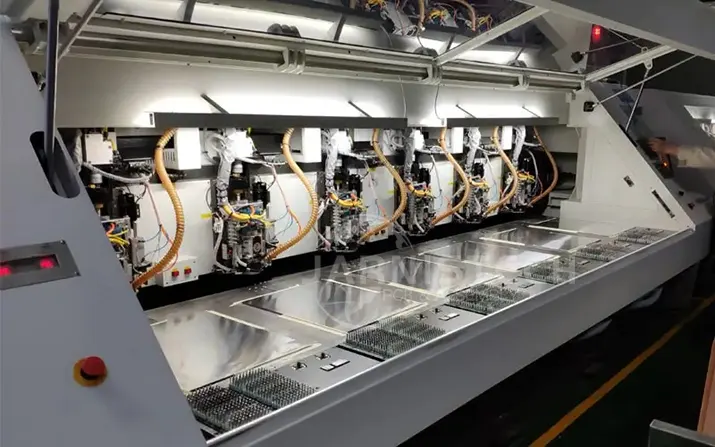
Essential Tools and Equipment for Functional Electrical Testing
Functional Electrical Testing requires a wide range of specialized tools and equipment to ensure the effectiveness and accuracy of the test. The proper tools not only streamline the testing process but also help us maintain high-quality standards. Whether you’re testing PCBs or PCBAs, selecting the right tools is a game-changer in achieving optimal results. Let’s dive into the essentials, from test benches and fixtures to automated equipment that can transform your testing workflow.
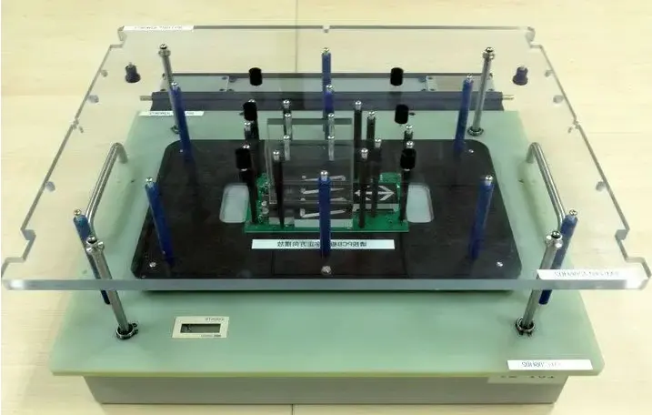
Test Benches and Fixtures for PCB Functional Electrical Test
When discussing PCB Functional Electrical Testing, test benches and fixtures are core components that ensure the entire process runs smoothly. These setups provide the physical connection between the PCBA and the testing system, replicating real-world conditions for accurate testing. A well-designed test bench or fixture can make a world of difference in enhancing test precision, speeding up the process, and minimizing the chances of human error. By using a thoughtfully constructed testing environment, we can ensure they get consistent, reliable results—without the guesswork. So, whether you’re troubleshooting or ensuring quality, having the right test bench in place makes all the difference!
The best practices for designing these platforms include incorporating adjustable mounting systems, efficient routing for electrical connections, and temperature control mechanisms. The test bench should be built with flexibility in mind to accommodate different board sizes and configurations. Moreover, features like built-in power supplies, oscilloscope integration, and programmable controllers are elements that enhance functionality.
Key Elements for PCB Test Bench Design-
| Component | Purpose | Impact on Testing Process |
| Adjustable Mounting | Supports various PCB sizes and shapes | Provides flexibility and reduces setup time |
| Oscilloscope Integration | Monitors signal integrity during testing | Helps to identify faults in real time |
| Programmable Controllers | Automates test cycles for efficiency | Increases repeatability and accuracy |
| Temperature Control | Simulates environmental testing conditions | Ensures reliability under varying conditions |
With a well-designed test bench, you’ll not only improve the speed of testing but also ensure the accuracy of the results. It’s all about optimizing your workflow for smoother operations!
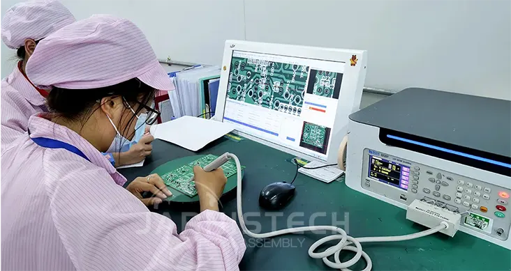
Selecting the Right Tools for PCBA Functional Electrical Testing
Selecting the right tools for PCBA Functional Electrical Testing is a major factor in accurately assessing the performance of your assemblies. The tools you use should align with the specific needs of the testing process, ensuring precise measurements and reliable component testing. Proper equipment helps detect issues with circuit connections, component functionality, and overall assembly performance. Without the right tools, it’s easy to miss potential flaws. By using high-quality, well-suited tools, you can identify problems early and ensure your PCBA functions as intended.
A few essential tools for PCBA FET include:
●Multimeters: Used to measure voltage, current, and resistance, multimeters are basic but indispensable in PCBA testing.
●Automated Test Equipment (ATE): These systems are used to conduct extensive, repeatable tests on PCBA. With ATE, testing can be done on multiple boards simultaneously, drastically reducing testing time.
●Signal Generators: These are used to simulate the operating conditions for components on the PCBA to verify their functionality under various frequencies.
By using specialized testing equipment tailored to PCBA FET, we can ensure more accurate, reliable results, while minimizing human intervention and errors.
Recommended Tools for PCBA FET-
| Tool | Function | Benefits for Testing |
| Multimeter | Measures voltage, current, resistance | Provides quick checks of basic electrical properties |
| Automated Test Equipment | Conducts repeated tests on multiple boards | Saves time and reduces manual errors |
| Signal Generators | Simulates real-world operational conditions | Verifies circuit functionality across frequencies |
It’s all about selecting the tools that are up to the task—no shortcuts, just solid equipment for optimal performance!
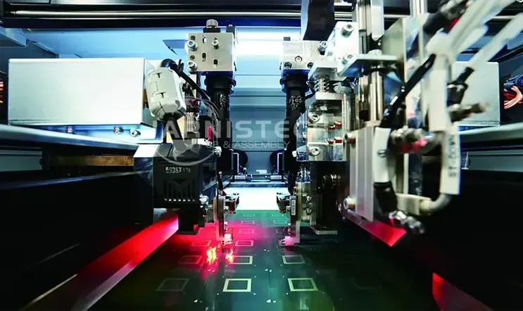
Innovations in Automated Testing Equipment for Functional Electrical Test
The testing landscape is rapidly evolving, and automated testing equipment has become a player in PCBA Functional Electrical Testing. These innovations streamline the process, allowing for more precise testing with minimal human input. By automating the testing procedures, we can achieve consistent results and speed up the testing phase, all while reducing the likelihood of error.
One such innovation is in-circuit testing (ICT) systems, which can conduct electrical tests on individual components of a PCBA while it is still on the assembly line. Another notable advancement is the flying probe tester, which uses probes to directly access specific points on the PCBA for detailed testing without the need for custom fixtures.
Additionally, automated optical inspection (AOI) systems are becoming increasingly popular for visual testing, using cameras and machine vision software to check for defects like solder joint issues, component misalignment, and incorrect component placements.
Automated Testing Innovations-
| Technology | Advancements | Impact on Testing Process |
| In-Circuit Testing (ICT) | Tests individual components in real time | Allows for quick detection of faults before the board moves further down the line |
| Flying Probe Testers | Direct testing of PCBA with no custom fixtures | Reduces setup time and increases flexibility |
| Automated Optical Inspection (AOI) | Visual inspection using cameras and software | Ensures no defects are overlooked, improving accuracy |
These innovations aren’t just about speed—they’re about getting the job done right, every time, while pushing the boundaries of PCBA FET!
Step-by-Step Implementation of PCB Functional Electrical Test
When it comes to ensuring the quality and reliability of your PCB or PCBA products, having a well-planned and executed Functional Electrical Test process is a must. A successful PCB Functional Electrical Test ensures that each board meets the necessary electrical standards before it’s sent out for final assembly or used in production. Let’s walk through the process of implementing FET, from preparation to testing procedures, all the way to post-test analysis. Each step plays a role in perfecting the test process for the highest quality outcome.
Preparing for a Successful PCB Functional Electrical Test
Preparation is half the battle. When setting up for a PCB Functional Electrical Test, a few core elements need to be in place to ensure everything runs like a well-oiled machine. You want to make sure that both the physical and technical environment is set up to allow for smooth testing without any hitches.
Set up your testing station by ensuring all tools, equipment, and safety measures are ready to go. Keep the area tidy and organized, free from unnecessary items that might get in the way. Make sure your workspace includes essentials like power supplies, multimeters, and the specific fixtures needed for PCBA FET. Double-check that the PCBA design documents and specifications are readily available, as they’ll act as your roadmap during the process. A well-prepared environment minimizes errors, saves time, and keeps the workflow running like a well-oiled machine. This proactive approach ensures you’re geared up to tackle testing tasks efficiently and effectively.
●Environmental Conditions: Temperature and humidity levels can affect the performance of the components, so control these factors to avoid skewed results.
●Test Setup: Verify that your test fixtures and equipment are correctly configured and ready to handle different board types and complexities.
Key Preparation Steps for a Successful PCB FET-
| Step | Action | Expected Outcome |
| Confirm Test Specifications | Review design and performance specs | Ensure accuracy in test setup |
| Prepare Testing Area | Clear workspace, set up equipment | Prevent test interruptions |
| Ensure Correct Environmental Conditions | Control temperature and humidity | Reliable and repeatable results |
By taking the time to set everything up properly, you’ll avoid delays and get more accurate results during the actual testing phase. It’s all about setting the stage for success!
Common Procedures in Functional Testing for PCB and PCBA
The core of Functional Electrical Testing lies in the methods used to evaluate various features of a PCB or PCBA. Mastering these techniques ensures that the testing process delivers reliable insights into the performance of your assemblies. The specific procedures may vary between PCB and PCBA testing, influenced by factors such as the complexity of the design and the characteristics of the components involved. By tailoring the approach to fit the assembly’s requirements, you can pinpoint issues effectively and make informed decisions about product quality. When it comes to nailing the details, understanding these processes is like having your ducks in a row—everything flows smoother and faster.
1.Initial Power-on Testing: After assembly, applying power to the board is the first step. This tests whether the PCBA powers up as intended and whether the voltage and current measurements match the expected values.
2.Signal Integrity Testing: This checks if the electrical signals pass through the circuit as expected, without distortion or interference. Common tools for this include oscilloscopes and signal analyzers.
3.Functional Verification: At this stage, the board is tested in real-world conditions to ensure each component performs according to its specifications. This step may involve using automated test equipment (ATE) to simulate operational scenarios.
Typical PCB FET Procedures-
| Test Phase | Action | Purpose |
| Initial Power-on Test | Apply power to the board and check voltages | Ensure basic functionality |
| Signal Integrity Test | Use oscilloscope to check signal quality | Identify any electrical faults |
| Functional Test | Verify each component’s operation | Confirm full circuit functionality |
These tests are often automated for efficiency, but the underlying principles remain the same: identify and resolve any faults that might impact the PCBA’s overall function. This is where your investment in good test tools pays off.
Post-Test Analysis and Reporting for Improved Quality Assurance
After the testing wraps up, the spotlight shifts to diving into the data and crafting detailed reports. This post-test analysis sheds light on how the PCB or PCBA held up under scrutiny and highlights areas that could use some fine-tuning. This stage is where all your quality checks come together, translating raw test results into actionable insights. Think of it as connecting the dots to see the bigger picture—every tweak you identify here lays the groundwork for a smoother ride down the production line.
Start by reviewing the test results and comparing them to the PCBA specifications. If any discrepancies are found, it’s essential to investigate further to determine whether there are issues with the design or manufacturing process. Often, failures in testing can point to weak points in the production chain, which can then be addressed for future runs.
●Data Interpretation: The test data needs to be interpreted in light of your design and performance specifications. If your results deviate from the expected, it might indicate a flaw in the PCBA’s design or component choices. This requires a deep dive into both the test results and the production line to figure out what went wrong.
●Continuous Improvement: The ultimate goal of post-test analysis is to improve future testing procedures and production runs. You may need to adjust the test protocols, refine the PCB design specifications, or even upgrade your testing equipment to achieve better results over time.
Post-Test Actions for Enhanced QA-
| Action | Purpose | Impact on Quality Assurance |
| Analyze Test Results | Compare against specifications | Spot deviations and pinpoint issues |
| Investigate Design or Manufacturing Issues | Identify root causes of failures | Enhance future design and production processes |
| Update Testing Procedures | Refine test methods based on analysis | Improve accuracy and efficiency for future tests |
This stage is where quality assurance steps in, ensuring that any issues are identified and corrected, setting the stage for even higher-quality products in the future.
Challenges and Solutions in PCBA Functional Electrical Testing
Conducting PCBA Functional Electrical Tests can bring about a variety of challenges that interfere with the workflow and product dependability. Issues such as physical defects, inconsistent outcomes, or limitations in testing equipment can lead to setbacks and disruptions. Identifying the underlying causes of these problems and implementing practical solutions is the way to keep everything on track. Let’s explore common challenges in testing and outline straightforward strategies to address them effectively.
Identifying Common Failures During PCBA Functional Tests
One of the most challenging aspects of PCBA Functional Electrical Testing is identifying the various failures that may occur during the test process. Failures can either be electrical (circuit faults, signal integrity issues) or physical (component placement, soldering defects). Both types can lead to inaccurate test results and ultimately compromise the quality of the PCBA.
●Electrical Failures: These typically involve issues like poor connections, signal interference, and incorrect voltages. Common culprits include damaged traces, faulty components, or poor soldering that doesn’t create a solid connection between the components and the PCB.
●Physical Failures: These failures are often related to improper component placement or defects in the solder joints. A misaligned component or a weak solder connection can lead to inconsistent performance or total failure during the test.
Common Failures in PCBA FET-
| Failure Type | Cause | Impact on Test Results |
| Electrical Faults | Broken traces, faulty components | Inaccurate voltage/current readings |
| Signal Integrity Issues | Cross-talk, poor connections | Distorted signal readings |
| Component Placement Errors | Misaligned or missing components | Board failure to function correctly |
| Soldering Defects | Cold joints, excessive solder | Poor electrical connection, unreliable test |
Tip: If you’re dealing with physical or electrical failures, check the assembly process. In many cases, issues stem from improper manufacturing practices. Ensure thorough inspection of the PCBA before it goes through testing.
Strategies for Overcoming False Positives in Functional Electrical Test
False positives—where a PCBA passes the test despite having underlying issues—can cause serious problems down the line. These false readings typically occur due to limitations in the test setup or due to improper calibration of test equipment. Tackling this issue requires a more advanced approach.
1.Test Fixture Design: Ensure your test fixtures are properly aligned and capable of accurately detecting faults. Poorly designed fixtures can cause inconsistent contact with the PCBA, leading to false positives. Invest in high-quality, precision test fixtures that can provide stable and reliable connections to the board.
2.Improved Test Equipment: Use more advanced automated testing equipment that can simulate real-world conditions. This reduces the likelihood of missing subtle defects that can cause issues later in the product lifecycle.
3.Test Coverage Expansion: Ensure that all necessary circuits are tested, including the most critical ones that directly affect performance. Expanding the test coverage can help catch failures that might otherwise go unnoticed.
Strategies to Reduce False Positives-
| Strategy | Action | Result |
| Test Fixture Improvement | Upgrade test fixtures for better accuracy | Reduces false positives from poor connections |
| Advanced Test Equipment | Use ATE (Automated Test Equipment) for more thorough testing | Improves fault detection capability |
| Expanded Test Coverage | Test all critical circuits and components | Increases the chances of detecting hidden defects |
These steps, although time-consuming, are necessary to improve the test’s precision. Remember, it’s about quality over speed!
Enhancing Test Accuracy with Calibration and Maintenance
The reliability of PCBA Functional Electrical Test outcomes heavily depends on the condition and calibration of the testing equipment. If the tools aren’t fine-tuned or kept in good shape, the results can easily deviate, leading to a skewed understanding of the assembly’s actual performance. Regular calibration ensures that measurements align with real-world benchmarks, while consistent upkeep of fixtures and tools prevents inconsistencies from creeping into the process. Neglecting these steps can turn what should be a smooth operation into a troubleshooting marathon, adding unnecessary headaches to your workflow.
1.Regular Calibration: Calibration ensures that your test equipment provides accurate readings. Over time, test instruments can drift, leading to skewed results. By regularly calibrating your equipment, you ensure that readings remain reliable throughout the entire testing process.
2.Routine Maintenance: Test equipment and fixtures wear out over time, leading to decreased performance. Regular maintenance checks can identify issues such as worn-out cables or malfunctioning probes, which can impact test accuracy.
3.Environment Control: The conditions in which PCBA Functional Electrical Tests are performed can have a big impact on the reliability of the results. Variations in temperature, exposure to static electricity, and other environmental factors can interfere with both the test equipment and the assembly under evaluation. To avoid any hiccups, it’s essential to create a controlled environment that minimizes these disruptions. Think of it like giving your tests the perfect stage to perform—consistent temperatures, proper grounding, and a setup free from outside interference help ensure the results truly reflect the PCBA’s capabilities.
Calibration and Maintenance Best Practices-
| Practice | Action | Benefit |
| Regular Calibration | Calibrate equipment at specified intervals | Ensures accurate test results |
| Routine Equipment Checks | Inspect and replace worn parts | Prevents faulty test equipment |
| Environmental Control | Control temperature and humidity in test areas | Minimizes test result discrepancies |
By staying on top of these practices, you’re ensuring that your PCBA Functional Electrical Test remains as accurate and reliable as possible, thus protecting the integrity of your final product.
Trends in PCB and PCBA Functional Electrical Testing
As the electronics industry pushes forward, PCB and PCBA Functional Electrical Testing (FET) must evolve to meet the demands of advanced technology. The trends in testing are continuously changing, and manufacturers must stay ahead of the curve to keep up with new challenges. Today, we’re diving into three of the most significant trends that are reshaping the landscape of PCB FET—artificial intelligence (AI), sustainability, and high-frequency testing.
The Role of AI and Machine Learning in Functional Electrical Test
AI and machine learning (ML) are no longer just buzzwords; they’re becoming a fundamental part of the PCB and PCBA testing process. These technologies are changing the way tests are performed by automating data analysis, improving accuracy, and enhancing test efficiency.
●AI-Powered Automation: In PCB FET, AI is used to analyze vast amounts of test data quickly. This allows the system to predict potential failures based on patterns and trends detected in previous tests, providing our engineers with insights they wouldn’t have been able to identify manually. The result? Faster identification of flaws and a reduction in the number of false positives.
●Machine Learning Models: Through machine learning, testing equipment can “learn” from past tests and adapt its testing parameters to improve future test results. For example, an ML model could identify trends in failures, enabling automatic adjustments to test conditions that better simulate real-world scenarios.
●Predictive Maintenance: With AI, maintenance schedules for test equipment can be predicted based on performance data, reducing downtime and ensuring the reliability of PCBA FET equipment.
Benefits of AI and Machine Learning in PCB Functional Electrical Testing-
| Technology | Benefit | Impact |
| AI-Powered Data Analysis | Faster data processing, improved fault detection | Reduces test time and increases accuracy |
| Machine Learning | Adapts to test results, learns from failures | Improves future test performance |
| Predictive Maintenance | Anticipates equipment failures | Minimizes unplanned downtime |
Sustainable Approaches to PCB Functional Electrical Testing
Sustainability isn’t just a buzzword—it’s a reality in the PCB testing industry. As environmental concerns grow, green technologies are becoming more prevalent in PCBA Functional Electrical Testing. These methods not only contribute to environmental conservation but also align with global regulations aimed at reducing e-waste.
●Energy-Efficient Test Equipment: Manufacturers are increasingly turning to energy-efficient test equipment that consumes less power, reducing the environmental impact of testing. This includes low-energy systems for data acquisition, power supplies, and automated test systems.
●Waste Reduction: With a focus on reducing waste, testing equipment now uses fewer consumables, such as disposable test leads and materials that wear out after several uses. Instead, reusable and recyclable options are becoming the norm.
●Green Testing Practices: In PCBA FET, manufacturers are focusing on reducing harmful chemicals and materials used during testing. Lead-free soldering and reducing hazardous substances in the testing process are key goals for many companies today.
Sustainable Approaches in PCBA FET-
| Green Practice | Action | Environmental Impact |
| Energy-Efficient Testing | Use of low-power automated testing equipment | Reduces overall energy consumption |
| Waste Minimization | Adoption of reusable test fixtures and materials | Decreases landfill waste |
| Lead-Free Soldering | Implement lead-free testing procedures | Decreases harmful material use |
Pro Tip: Going green in your testing processes not only helps the environment but can also enhance your brand’s reputation as a responsible manufacturer. So, why not take the first step toward a more sustainable future?
High-Frequency and RF Testing Techniques in Modern PCB Designs
As PCB designs evolve to handle faster data transfer speeds, higher frequencies, and more complex signal processing, the need for high-frequency testing has become a necessity. Whether it’s a RF PCB, 5G components, or high-speed circuits, new testing methods are required to ensure that these advanced designs meet their specifications.
●High-Frequency Signal Testing: In high-frequency PCB designs, traditional testing techniques often fail to accurately detect signal issues like reflections, loss, or interference. Advanced techniques such as time-domain reflectometry (TDR) and network analyzers are becoming increasingly popular for measuring high-speed signals.
●RF Testing Equipment: For PCBA FET, RF test systems are used to evaluate the integrity of PCB traces and components in the high-frequency spectrum. These systems are designed to test the RF performance of PCBs in conditions that simulate real-world RF environments, such as 5G networks.
●Minimizing Signal Loss: High-frequency testing also involves analyzing signal loss and ensuring that PCB designs are optimized for minimal signal degradation. This includes carefully monitoring trace impedance, via design, and component placement to prevent signal loss in RF circuits.
High-Frequency Testing in PCB FET-
| Testing Technique | Action | Impact |
| Time-Domain Reflectometry (TDR) | Measures signal reflections to detect faults | Identifies impedance mismatches and losses |
| Network Analyzers | Tests RF circuit performance across frequencies | Ensures signal integrity in high-speed designs |
| Impedance Control | Optimizes trace layout to minimize signal loss | Reduces signal degradation in high-frequency circuits |
Tip: As PCBA designs evolve and tackle higher frequencies, incorporating specialized RF testing equipment is a must. If you’re dealing with high-speed designs, don’t skip out on advanced test techniques—they’ll save you from issues down the road.
Ensuring Long-Term Reliability with Functional Electrical Test
When it comes to PCB and PCBA Functional Electrical Testing (FET), it’s not enough to simply pass initial tests. The ultimate goal is to ensure the long-term reliability of the product. Whether it’s through stress testing, lifecycle testing, or IoT and wearable device adaptations, these methods are designed to simulate real-world conditions and ensure your PCB or PCBA functions flawlessly throughout its lifespan. In this section, we’ll explore key testing strategies that guarantee a product’s durability and dependability over time.
Stress Testing During PCB Functional Electrical Tests
Stress testing in PCB Functional Electrical Testing involves pushing components and circuits beyond their usual operating limits to evaluate how they perform under tough conditions. This type of testing helps to uncover any potential weaknesses that may not show up under normal circumstances. Whether it’s dealing with high temperatures, humidity, or extreme electrical loads, stress testing ensures the PCB can handle the real-world pressures it will face once deployed. It’s all about making sure that when the heat is on, your PCB is tough enough to take it, ensuring long-term durability and reliable performance.
●Environmental Stress Testing: This includes thermal cycling and high/low temperature tests to simulate extreme temperature shifts, which could occur in applications like automotive electronics, or devices exposed to outdoor elements. The PCB is subjected to high temperatures, freezing conditions, and rapid temperature changes to evaluate performance under stress.
●Electrical Stress Testing: Components on the PCB are tested under electrical loads that exceed normal operation levels, ensuring that they can handle surges, spikes, or other unforeseen electrical conditions.
●Mechanical Stress Testing: Flexing, vibration, and shock tests simulate conditions in which the PCB might experience physical stress, whether from transportation, device usage, or manufacturing processes.
Stress Testing Procedures-
| Test Type | Test Condition | Impact |
| Thermal Cycling | Subject PCB to extreme temperature changes | Identifies weaknesses in solder joints and materials |
| Electrical Overload | Simulate power surges or voltage spikes | Ensures components can withstand electrical extremes |
| Vibration/Shock Testing | Expose PCB to mechanical shock and vibrations | Assesses structural integrity and robustness |
Don’t let your PCBA fail when it counts most. Incorporate stress testing into your routine to catch hidden flaws before they become a problem. Test harder to ensure reliability!
Lifecycle Testing in PCBA Functional Electrical Tests
Lifecycle testing ensures that a PCBA can withstand the wear and tear of its entire service life. From the moment a product leaves the factory to its final days of operation, lifecycle testing verifies that it will perform consistently under different environmental and electrical conditions.
●Accelerated Life Testing (ALT): ALT involves subjecting the PCBA to conditions that speed up the aging process, such as high temperatures, constant electrical loads, or repetitive mechanical stress. This helps engineers predict the product’s longevity and identify potential failure points.
●Long-Term Exposure Testing: This type of testing involves placing the PCBA in real-world environments over extended periods to simulate the actual wear and tear a device experiences. This includes everything from environmental exposure to human interaction, to ensure that the device performs consistently over time.
●Corrosion Testing: For PCBA that may be exposed to moisture or harsh chemicals, corrosion testing helps simulate long-term exposure to these factors, ensuring that the board’s components remain functional despite adverse environmental conditions.
Lifecycle Testing Considerations-
| Test Type | Test Method | Benefit |
| Accelerated Life Testing | High-temperature, constant electrical load exposure | Identifies potential weak points before product release |
| Long-Term Exposure | Real-world environmental and usage simulations | Predicts product lifespan and durability |
| Corrosion Testing | Exposure to moisture or chemicals | Ensures longevity of products in harsh environments |
Pro Tip: Don’t cut corners when it comes to lifecycle testing—ensure your PCBA lasts as long as your customers need it to. A little extra testing now can save you big-time repairs and customer complaints later!
Enhancing Reliability for IoT and Wearable Devices Through FET
The surge in IoT (Internet of Things) and wearable devices has introduced a host of new challenges for PCBA Functional Electrical Testing. These devices face various conditions, such as body heat, sweat, humidity, and dust. As a result, ensuring their long-term durability through comprehensive testing is more pressing than ever. Through thorough FET (Functional Electrical Testing), we can reinforce the reliability of these devices, ensuring they withstand demanding environments. Rigorous testing helps minimize unexpected failures and boosts overall product quality, ensuring these devices continue to meet user expectations no matter the circumstance.
●IoT Device Testing: As IoT devices become more integrated into daily life, it’s necessary to conduct thorough tests for connectivity, energy efficiency, and durability in challenging conditions. These tests should focus on aspects such as signal integrity, RF interference, and battery longevity, ensuring the device meets real-world demands. The goal is to guarantee that your product performs consistently, without unexpected issues, over time. By executing these tests properly, you set your product up for long-term success, with no surprises down the road.
●Wearable Device Testing: Wearables are exposed to unique conditions—body motion, perspiration, temperature fluctuations, and even drops or shocks. To ensure these devices perform reliably, PCBA FET must include mechanical stress testing, moisture resistance, and power management testing.
●Durability Testing for Small Form Factor Designs: Since IoT and wearable devices often feature compact PCBA designs, testing the durability of these small form factors is a must. Rigorous testing ensures that delicate components can handle constant movement, bending, and exposure to a variety of conditions. These tests simulate real-life scenarios to make sure the assembly can stand up to everyday wear and tear. It’s about making sure that no matter what life throws at the device, it keeps performing as expected.
IoT and Wearable Device FET-
| Device Type | Test Focus | Goal |
| IoT Devices | Connectivity, low-power operation, signal integrity | Ensures reliable performance in diverse environments |
| Wearable Devices | Moisture resistance, mechanical shock, power efficiency | Optimizes performance during everyday use |
| Small Form Factor | Durability of miniaturized components | Ensures longevity and robustness in tight spaces |
Whether it’s an IoT device or a wearable, the goal is to test these products under real-world conditions to ensure they perform well in the long run. To stay ahead of the competition, it’s important to conduct PCBA Functional Electrical Tests that factor in the full user experience. By evaluating how the product behaves in real-life scenarios, you ensure it’s prepared for anything and will meet expectations under various conditions.
Best Practices for Functional Electrical Test Optimization
Optimizing Functional Electrical Testing (FET) for PCB and PCBA involves striking the right balance between cost efficiency, test coverage, and performance. When done right, FET not only guarantees product reliability but also streamlines production processes, reducing unnecessary costs. In this section, we will dive into key best practices for optimizing your FET process, ranging from balancing costs with quality to embracing automation and continuous improvements.
Balancing Cost and Quality in PCB Functional Electrical Testing
In PCB Functional Electrical Testing, finding a sweet spot between cost and quality can be tricky, especially when you want to ensure comprehensive testing while keeping production costs in check. Here’s how to balance the two without compromising performance:
●Test Prioritization: Begin by evaluating the most critical aspects of the PCB’s functionality. Focus on high-risk areas that could cause failure down the line, such as power circuits, high-speed traces, and sensitive components. Testing only these high-priority elements can significantly reduce costs while ensuring the device functions as intended.
●Test Coverage vs. Cost: Sometimes, less is more. Instead of testing every possible function, concentrate on the most vital features. It’s tempting to run exhaustive tests, but in high-volume manufacturing, optimizing test coverage to ensure core functionality can be a more cost-effective approach. For example, boundary scan tests and automated functional tests can pinpoint the most common failures without excessive testing time.
●Testing Technology: Using in-circuit testers (ICT) or flying probe testers in conjunction with functional tests helps lower initial investment while still providing accurate results. These tools allow for faster test execution and easier adaptation to different designs, minimizing downtime and testing expenses.
Cost vs. Quality in PCB FET-
| Factor | Optimized Approach | Impact |
| Test Prioritization | Focus on critical components and high-risk areas | Reduces testing time and costs |
| Test Coverage | Limit tests to the most vital functions | Ensures quality while reducing unnecessary tests |
| Test Technology | Use automated and flexible testing equipment (ICT, flying probes) | Increases speed and reduces operational costs |
When you’re juggling cost and quality, always start by understanding what truly matters for your PCBA. Pinpoint the high-stakes areas and optimize your testing for speed and accuracy. Less can be more if done strategically!
Automating PCBA Functional Electrical Test in High-Volume Production
In high-volume production settings, automation is the secret sauce for boosting efficiency while keeping the accuracy of PCBA Functional Electrical Tests on point. Automation helps eliminate human error, speeds up testing cycles, and ensures that every unit is tested consistently. . Here’s how automation technology can streamline the process:
●Automated Test Equipment (ATE): ATE systems are designed to automate PCBA testing, from initial setup to data collection. These systems provide high-speed testing while minimizing human error. Automated test fixtures, coupled with pick-and-place machines, offer fast, reliable, and repeatable results.
●Test Integration: In a high-volume scenario, automated test systems can integrate directly with production lines. This means that tests are conducted automatically as PCBs are assembled and moved along the production line, ensuring real-time verification of quality. Integration helps eliminate delays and reduces the risk of defective units slipping through.
●Data Analytics for Continuous Improvement: With automated testing, data analytics become an integral part of the process. Automated tests generate a wealth of performance data that can be used to identify patterns, troubleshoot issues, and make real-time adjustments to the process. Over time, this feedback loop results in continuous improvement of both the product and the production process.
Automation in High-Volume FET-
| Aspect | Benefit of Automation | Impact |
| Automated Test Equipment | High-speed, reliable testing with minimal human intervention | Reduces labor costs and increases throughput |
| Test Integration | Real-time testing during assembly | Prevents defects and improves quality control |
| Data Analytics | Real-time monitoring and performance adjustments | Continuously optimizes the testing process |
Pro Tip: Implement automation where it makes the most sense: on the production line. Automated PCBA FET minimizes delays, prevents human error, and ensures that quality is maintained at scale. Don’t wait—automate to dominate!
Continuous Improvement Strategies for Functional Electrical Tests
No process is ever perfect, which is why continuous improvement is a must when it comes to Functional Electrical Testing. Here’s how to use feedback and data to optimize your FET process over time:
●Root Cause Analysis: When a failure occurs during testing, it’s important to go beyond simply fixing the issue. A detailed root cause analysis helps identify underlying patterns or systemic issues that may be affecting the testing process or the PCB design itself. This approach helps prevent recurring problems and ensures long-term quality.
●Closed-Loop Feedback: Use the data generated during functional testing to make continuous improvements. Establish a closed-loop feedback system where test results inform adjustments in the design, production, or testing processes. By integrating testing results into every stage of development, you can continuously refine the product and improve overall quality.
●Employee Training and Best Practices: Ensure that the team conducting the tests is trained in the latest techniques and technologies. Employees should be equipped with the skills to interpret test data, adjust parameters, and spot issues that could affect testing accuracy.
Continuous Improvement in PCB FET-
| Strategy | Benefit | Impact |
| Root Cause Analysis | Identifies underlying issues that affect quality | Prevents recurring failures and improves testing reliability |
| Closed-Loop Feedback | Data from testing informs continuous product/process improvements | Ensures ongoing optimization and quality refinement |
| Employee Training | Trains testers in advanced techniques and process improvement | Enhances test accuracy and ensures long-term success |
Final Tip: The best way to keep your FET process efficient is by always iterating. Continuously collect data, train your team, and adjust your testing methods based on insights. Continuous improvement isn’t just a strategy—it’s a mindset!
Why Choose Us to Become Your High-Quality PCB Manufacturer?
When it comes to PCB manufacturing, there’s no room for error. Precision and quality are non-negotiable. With JarnisTech, you’re not just choosing a vendor—you’re picking a reliable partner who gets the fine balance between top-notch quality, sharp precision, and speed. We’re here to bring your designs to life with accuracy and dependability, so you can move forward without a hitch.
Choose JarnisTech for PCB Testing
PCB testing is an integral part of the design and manufacturing process. Whether you’re running tests to validate a new prototype or scaling up for high-volume production, the testing phase is where errors get caught before they cause costly production delays. Selecting a manufacturer for PCB testing can make a real difference, and JarnisTech already bring the precision and know-how to meet your needs.
Why JarnisTech?
1.Reliability You Can Trust-
At JarnisTech, we understand that the quality of your PCBs directly impacts the success of your products. That’s why we are committed to delivering top-quality prototypes and small-scale production runs with meticulous attention to detail. From functional electrical tests (FET) to stress testing, we make sure that every unit that leaves our facility meets or exceeds your expectations.
2.Proven Expertise in High-Quality Prototyping-
We offer rapid prototyping services that speed up the testing process without compromising on quality. Our seasoned engineers and advanced equipment ensure that every prototype we produce is exactly as per your design requirements, guaranteeing smooth testing in the next phase.
3.Transparent Pricing—No Hidden Fees-
We believe in being straightforward with our clients. There are no surprises, no hidden charges—just competitive pricing for unparalleled quality. This transparency ensures you can confidently plan your budget and timelines without worrying about unexpected costs.
4.Streamlined Production Process-
Our optimized manufacturing processes are designed to save you both time and money. By choosing JarnisTech, you’re partnering with a team that values efficiency as much as you do. Our automated testing systems provide fast, accurate results with minimal manual intervention, helping to move your designs to the next stage faster.
5.Comprehensive Testing Services-
Whether you’re dealing with high-frequency PCBs, IoT devices, or wearable technologies, we tailor our testing protocols to your specific needs. Our services include electrical testing, signal integrity testing, thermal cycling, and more, ensuring your PCBs will perform flawlessly under real-world conditions.
How We Can Help You Achieve Success?
●Fast Turnaround Times: In today’s competitive market, timing is everything. With JarnisTech, expect fast and accurate testing that helps you meet tight deadlines without compromising on quality.
●Flexible Production Runs: From prototype to small-batch production, we offer flexibility to meet the unique needs of each project. Whether you’re scaling up for mass production or need a quick batch for specialized testing, we’ve got you covered.
●Advanced Technology at Your Service: Our state-of-the-art testing and manufacturing facilities are equipped with the latest technology to guarantee the highest level of precision and efficiency. We stay at the forefront of industry advancements to ensure your PCBs are built using the most up-to-date techniques and tools.
Get Your Prototype Today—Start the Testing Process Right!
When you choose JarnisTech, you’re not just selecting a PCB manufacturer; you’re choosing a partner that’s dedicated to your success. We understand the value of accurate, efficient testing in delivering high-quality PCBs that work flawlessly every time.
Request a quote today and see how JarnisTech can help streamline your PCB testing process, saving you time and money, while ensuring your products are production-ready without the headaches. Don’t settle for less—partner with the best.


