
In order to increase the quality of PCBA production, producers must inspect the boards thoroughly. PCB (Printed Circuit Board) SMT (Surface Mount Technology) assembly inspection equipment should be utilized for a thorough and efficient in-depth board inspection.
The information provided by SPI, AOI, ICT, and AXI will allow you to optimize your boards and correct any problems for the maximum output quality possible. This article contrasts SPI, AOI, ICT, and AXI.
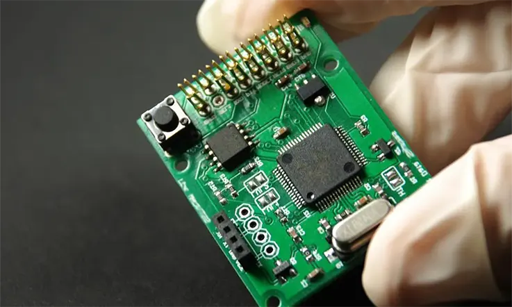
PCB Assembly Inspection and Testing: SPI, AOI, AXI, and ICT
PCB assembly inspection and testing engineers face far more challenges today than they did previously. The complexity of PCB boards is increasing as more components are mounted on board, more joints are added, densities are increased, and new package technologies such as area array packages and 0402 and 0201 chip components are introduced. Because of the higher component and joint numbers, there are more potential for defects, which results in lower yields for a given defect level.
At the same time, modern technologies like Automatic Optical Inspection (AOI), Solder Paste Inspection (SPI), and Automatic X-ray Inspection provide more inspection and testing options (AXI). These well-established inspection technologies offer genuine options for capabilities and advantages.
In addition to the In-Circuit Test (ICT) and Functional Test, Boundary-Scan Test Technology has also evolved as a prominent electrical testing method in recent years (FCT). During the process of PCB assembly, these key inspection and testing procedures provide more options for improving PCB assembly quality in prototypes and volume production.
Process for SMT, Inspection, and PCBA Testing
The process of assembling printed circuit boards (PCBs) normally consists of two stages: surface mount technology (SMT) and inspection, and printed circuit board assembly (PCBA) testing.
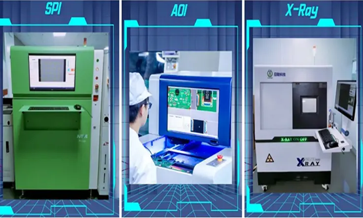
SPI Test (Solder Paste Inspection)
The application of solder paste is a step that plays a critical role in the manufacturing of printed circuit boards (PCBs). According to the findings of the research that was carried out, inappropriate solder paste application is responsible for more than 60 percent of all errors that arise during the period of mass manufacturing. It is possible that the “lifespan” of the system will be shortened or that it will not function correctly if the material is not distributed evenly.
Therefore, SPI tests make use of specialized technology that permits exact 3D and 2D image processing. By verifying the paste application technique in this manner, automated production line equipment may be configured more effectively. By doing this, you can cut the amount of flaws by as much as 60%. Therefore, it is not surprising that a huge number of manufacturers employ specialized tools and software for SPI testing.
AOI Test (Automated optical inspection)
Automated optical inspection, also known as AOI, is an automated visual inspection that is performed during the manufacture of printed circuit boards (PCB) (or LCDs, transistors). During this inspection, a camera performs a self-guided scan of the device being evaluated to look for both catastrophic failure (such as a missing component) and quality defects (e.g. fillet size or shape or component skew).
Because it is a form of testing that does not involve physical contact, it is frequently utilized in the production process. It is implemented at several stages throughout the manufacturing process, including bare board inspection, solder paste inspection (SPI), pre-reflow, and post-reflow, as well as other stages.
After solder reflow, often known as “post-production,” has traditionally been the principal location for automated optical inspection (AOI) devices. The primary reason for this is that post-reflow AOI systems can inspect for a wide variety of different types of flaws (including component placement, solder shorts, missing solder, and so on) at a single point in the assembly line using just a single system. In this manner, the boards that were found to be defective are reworked, and the boards that were not found to be defective are moved on to the subsequent stage of the process.
AOI and SPI Testing :What Are the Benefits ?
● Massive financial losses can be incurred by the manufacturer as a result of undetected flaws in the design and assembly of printed circuit boards (PCBs). When the elements are taken beyond the production stage, the potential costs increase by a factor of ten and may put the good reputation of the brand in jeopardy.
● Proven methods for finding even the tiniest faults include using advanced AOI and SPI testing. The limited capabilities of the human eye are no match for the precision and accuracy of specialized equipment. The potential for errors to occur during the PCB assembly process can be reduced to a minimum by carefully carrying out the tests. And as a consequence of this, the producer is able to keep manufacturing costs to a minimum, save time, and speedily offer new items to markets, all of which contribute to a maximizing of profits.
ICT Test (In-Circuit Testing )
The In-Circuit Test (ICT) gives us the ability to look for a variety of different types of failures, such as openings, shorts, continuity tests, and so on. There are two primary techniques for accomplishing it.
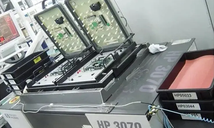
Flying probe test: This technique enables us to conduct tests with smaller diameters; we can attain a minimum test pitch of 0.2 mm. The PCB is placed in an environment for testing in which the various probes will make contact with the pads and vias. In addition to scanning for shorts and openings, the device is equipped with a camera that examines the size and shape of electronic components. It allows us to manage the absence of elements. Allows us to study the values of components such as resistance and capacitance, for instance. Additionally, it is possible to assess the polarity of the elements.
Bed of nails: This is a traditional test. It attempts to generate multiple contact points in the circuit using small spring-loaded pogo pins that, when viewed from a distance, resemble a bed of nails, hence the name. Each pogo pin will make contact with a cricut node, applying pressure to the Device Under Test (DUC) and testing hundreds of connections at the same time. Using this technique, we can detect component defects as well as parameter deviation, solder joint bridging, displacement, opens, shorts, continuity tests, and so on.
This kind of test is quick, cheap, and appropriate for both mass production systems and simple PCBAs. On the other hand, if we try to apply it to high-density components or large-scale integrated PCBs in which miniaturization has taken a leading role, we will discover that there are technological challenges that cannot be solved. Because of this, over the course of time, many methods have been developed to replace these types of examinations.
AXI Test (Automated X-ray Inspection)
AXI performs exceptionally well in electronics fabrication for printed circuit boards with visible joints. However, many modern PCBs include technologies such as BGA, BGA integrated circuits (ICs), and chip scale packages (CSPs) in which the solder connections are not visible by visual inspection methods such as naked eye and AOI. This is a result of the requirement for more interconnections in integrated circuit packages, as well as the general increase in complexity. In these and numerous other circumstances, X-ray technology is required for inspections.
Automated Optical Inspection (AOI) is extremely similar to Automated X-Ray Inspection (AXI), with the primary difference being that AXI processes X-Ray images using computer vision rather than optical images. Because of this, the test will be able to confirm all of the solder connections on the board once it has been assembled. This includes the solder joints that are hidden behind a component. This is useful for ensuring that ball grid array (BGA) components have been assembled correctly.
Comparing AOI, ICT, AND AXI
● The advantages of AOI include a great degree of flexibility and an enormously reduced amount of time spent programming tests. AOI is also capable of aggregating the manufacturing quality of each link as well as the type of defect that will be used by technology control engineers for analysis and management. The most significant drawbacks of AOI systems are an inability to detect invisible solder joints, a failure to detect circuit flaws, and the inability to inspect for problems that can only be observed with visual examination.
● ICT offers a number of benefits, including rapid test speed and high defect observation rates, among other advantages. Users that need huge volume products are the most likely to make use of it because of the speedy features and convenient design it offers. On the other hand, businesses that require a low volume of a varied range of products may not value ICT due to the fact that bed nails need to be changed frequently and it may be difficult to discover problems in complicated circuits that have a higher density.
● The AXI system is able to inspect solder junctions thoroughly, even those that are invisible to the human eye. The rate of manufacturing defects in their products might reach as high as 97%. A significant drawback is that AXI is unable to test for flaws in terms of its electrical performance. The capturing of images for the purpose of inspection is a category that AXI and AOI both fall under, making them part of the same category of structural testing and inspection. However, the most significant distinction is that AOI machines rely on light sources, whereas AXI machines rely on X-rays to acquire images.
Consequently, What Method of Inspection Should You Select? ICT, AOI, or AXI?
First, we have to keep in mind that we do not have to pick one over the other; rather, we just need to determine how and when we will combine the two of them, as well as for what purposes each of them will be used individually. This will be determined by the level of complexity of our PCB as well as the type of defect that we intend to check for.
Comparison of the Major Detection Capabilities of AOI, X-Ray and ICT | |||
| Defect Type | AOI | X-Ray | ICT |
| Soldering Defects | |||
| Open Circuits | Y | Y | Y |
| Soldering Openings | Y | Y | Y |
| Solder Shorts | Y | Y | Y |
| Insufficient Solder | Y (not heel of joint) | Y | N |
| Solder Void | N | Y | N |
| Excess Solder | Y | Y | N |
| Solder Quality | N | Y | N |
| Component Defects | |||
| Lifted Lead | Y | Y | Y |
| Missing Component | Y | Y | Y |
| Misaligned or Misplaced Component | Y | Y | Y |
| Incorrect Component Value | N | N | Y |
| Faulty Component | N | N | Y |
| BGA and CSP Defects | |||
| BGA Shorts | N | Y | Y |
| BGA Open Circuit Connections | N | Y | Y |
It is essential to have a thorough understanding of the many kinds of flaws that can be found using different kinds of inspections. This is demonstrated quite clearly in the table.
Noting that certain faults are only detectable through ICT, this test becomes essential.
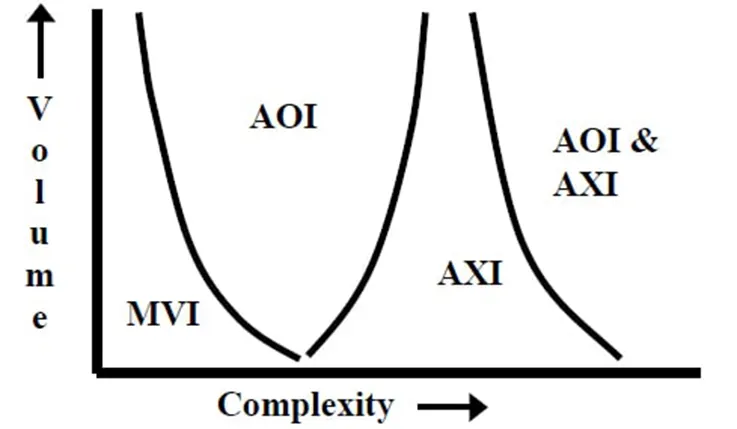
As a result, our choice of strategies will consist of either utilizing AOI, AXI, or a combination of the two. The graph that is currently being displayed can serve as a general guideline for us. It is important to note that a printed circuit board (PCB) need not be complicated so long as it contains BGA devices and you keep in mind the following: if the PCB has a BGA component, we can only study it in depth using X-ray technology. Manual Vision Inspection is what we refer to as MVI.
We also need to keep in mind that time is money, and as XAI is a slower inspection method in comparison to AOI, the cost of the pcba will be higher if we use it.
Final Words
PCB manufacturing requires a high level of quality control and uniformity, both of which can be ensured by utilizing our automated inspection solutions. The full spectrum of system solutions offered by us, including SPI (Solder Paste Inspection), AOI (Automated Optical Inspection), ICT (In-Circuit Test), and AXI (Automated X-ray Inspection) technologies, are able to fulfill the comprehensive inspection requirements of any PCB fabricate and assembly.


