Single-sided flexible printed circuits (FPCBs) facilitate the development of compact and dynamic electronic products. This guide is structured for product developers and procurement specialists, presenting a methodical examination of the full FPCB lifecycle—from material specification through to final assembly.
The contents cover:
●Material Selection
●Advanced Design Rules
●Manufacturing Processes
●Assembly Considerations
Fundamentals of Single-Sided Flexible PCBs
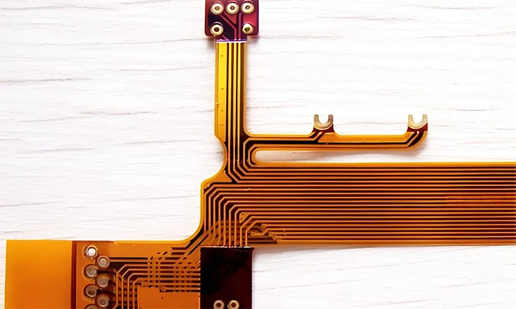
A single-sided flexible PCB is an interconnection device composed of a single conductive layer on a pliable polymer film. This construction is specifically engineered for applications where electronics must conform to non-planar spaces or withstand mechanical movement, providing a definite alternative where rigid boards are impractical.
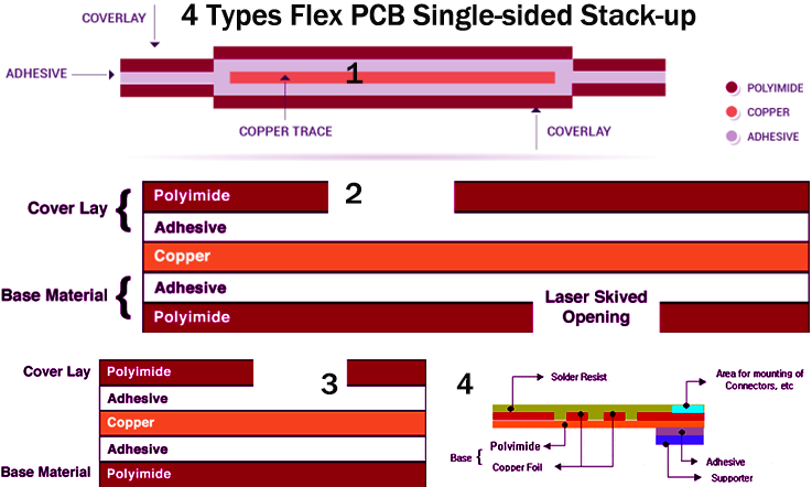
Core Construction and Layer Stack-up
The structure of a single-sided FPCB is a layered composite. The selection and arrangement of these materials govern the circuit’s mechanical properties, electrical performance, and manufacturability.
Structure of a Single-sided Flexible PCB:
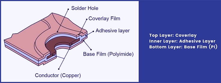
Base Dielectric Substrate:
This polymer film is the foundation of the circuit, providing mechanical support and electrical insulation. Polyimide (PI) is a common material choice due to its thermal resilience and robust physical properties.
Adhesive Layer:
In many designs, an adhesive bonds the copper conductor to the substrate. The characteristics of this adhesive influence the circuit’s flexibility, thermal behavior, and performance during assembly soldering processes. Adhesiveless constructions, which directly bond copper to the substrate, are available for applications requiring enhanced thermal or mechanical performance.
Conductor Layer:
A single sheet of thin copper foil forms the electrical pathways. This foil is chemically etched to produce the specified pattern of traces and pads. The copper’s type and thickness are selected based on current-carrying requirements and the needed flex endurance.
Cover Layer (Coverlay):
This protective polyimide film is laminated over the etched copper, serving a purpose similar to a flexible solder mask. It insulates the conductors from the operational environment and prevents solder bridging during the assembly phase. Openings are precisely created in the coverlay to provide access to solder pads.
Table: Single-Sided Flexible PCB Layer Composition
| Layer | Material Example | Typical Thickness | Primary Function |
| Base Substrate | Polyimide (PI) | 12–50 µm | Mechanical support, insulation |
| Adhesive Layer | Acrylic/Epoxy | 12–25 µm | Bond copper to substrate |
| Conductor Layer | RA or ED Copper | 9–35 µm | Electrical conduction |
| Coverlay | Polyimide + adhesive | 25–50 µm | Protection & insulation |
Comparison with Single-Sided Rigid PCBs
The choice between a flexible and a rigid circuit is dictated by the application’s physical and mechanical requirements. The comparison highlights distinct differences in form factor, performance, and total system cost.
Form Factor and Weight:
Flexible circuits have an exceptionally low profile and mass. This attribute is a determining factor in weight-sensitive applications, such as portable electronics and aerospace systems, capable of reducing interconnect weight substantially compared to traditional board-and-wire solutions.
Dynamic Flexing:
The capacity for repeated bending is a primary differentiator. A properly specified FPCB can endure a high number of flex cycles without conductor failure, a capability that rigid materials do not possess. This makes them suitable for devices with hinged or moving elements.
Three-Dimensional Packaging:
The ability to be folded and shaped to fit complex geometries enables highly integrated product assemblies. This can eliminate the need for separate components like connectors and cables, simplifying a device’s internal architecture.
Cost Dynamics:
While the initial unit price of a flex circuit can be higher than that of a simple rigid board, its use can result in a lower total system cost. This reduction is achieved by simplifying the assembly process, lowering the component count in the bill of materials (BOM), and removing potential points of failure associated with discrete wiring.
Table: Flexible vs. Rigid Single-Sided PCB Comparison
| Parameter | Flexible PCB (Single-Sided) | Rigid PCB (Single-Sided) |
| Thickness (typical) | 0.05–0.2 mm | 0.6–1.6 mm |
| Weight | Very low | Higher |
| Flex Durability | High (≥1 million cycles possible) | None (brittle under bending) |
| 3D Assembly Capability | Yes, foldable & shapeable | No, fixed flat form |
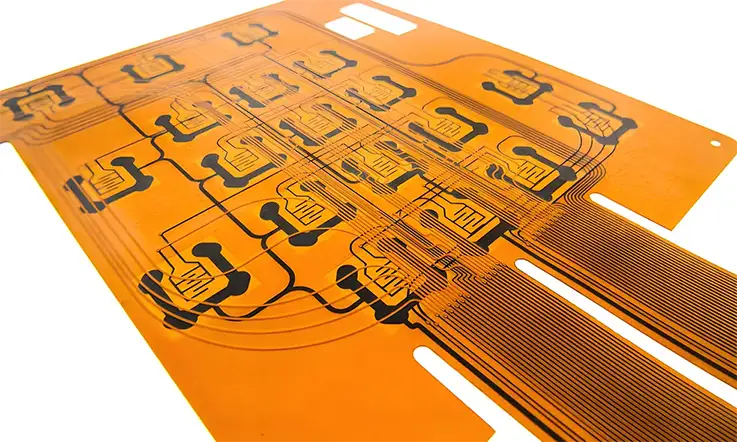
Single-Sided vs. Multilayer Flex: A Technical Comparison
Placing single-sided FPCBs in contrast with their multilayer counterparts helps define the specific application for each technology. The comparison clarifies the trade-offs in complexity, mechanical properties, circuit density, and cost.
Complexity and Layer Count
This is the fundamental structural difference. A single-sided FPCB has one conductive copper layer. In contrast, a multilayer FPCB integrates two or more conductive layers, separated by flexible dielectric material. These layers are interconnected with plated through-holes (vias) that pass through the substrates.
Thickness, Flexibility, and Bend Radius
The addition of copper and adhesive layers makes multilayer FPCBs thicker and less pliable, which directly affects their mechanical performance.
●Single-Sided: Offers the greatest flexibility and the tightest bend radius due to its minimal thickness. This makes it the superior selection for applications with continuous, dynamic flexing.
●Multilayer: Exhibits reduced flexibility from its composite structure. The minimum bend radius is larger, and its design requires careful management of internal stresses to prevent delamination or via failure during flexing.
Circuit Density and Routing Capability
The advantage of a multilayer construction is its increased capacity for complex circuitry.
●Single-Sided: All conductive traces must reside on a single plane, limiting routing density and potentially requiring a large surface area for high pin-count components.
●Multilayer: Enables highly complex and dense routing, as traces can cross on different layers. This allows for the interconnection of advanced processors and high-density connectors in a compact footprint. Dedicated inner layers can serve as ground and power planes, improving signal integrity and providing EMI shielding.
Cost and Manufacturing Process
The fabrication of a multilayer FPCB is substantially more involved, which is reflected in its cost.
●Single-Sided: Represents the most straightforward and cost-effective flexible circuit to produce, involving a single lamination and etching cycle.
●Multilayer: Requires multiple, precise steps such as via drilling (mechanical or laser), plating to form through-hole connections, and multi-stage lamination cycles, all of which increase production complexity and cost.
Application Profile
The selection is based on a clear balance of design requirements and performance needs.
1.Single-Sided Flex is the designated solution for:
●Simple point-to-point interconnections.
●Applications involving high-frequency or continuous dynamic flexing.
●Designs where minimal weight and thickness are specified.
●Projects where cost-effectiveness is a primary consideration.
2.Multilayer Flex is specified for:
●Complex circuit designs with a high density of components.
●Applications requiring controlled impedance with ground/power planes.
●Products that demand a high degree of EMI shielding.
Material Science: The Building Blocks of a Single-Sided Flex PCB
The performance and reliability of a single-sided FPCB are directly governed by the materials used in its construction. Each material choice represents a trade-off between cost, thermal properties, electrical characteristics, and mechanical durability.
Substrate Materials: Polyimide (PI) and Alternatives
The substrate material forms the physical structure of the flex circuit and dictates many of its performance characteristics.
●Polyimide (PI): As the industry standard, PI offers a superior combination of thermal stability (withstanding solder reflow temperatures), excellent dielectric strength, and high mechanical durability for dynamic applications.
●Polyethylene Terephthalate (PET): A lower-cost polymer, PET is suitable for applications that do not require high-temperature soldering and where cost is a primary consideration. Its flexibility is good, but its thermal and mechanical stability are lower than PI.
●Polyethylene Naphthalate (PEN): Offering performance characteristics between PET and PI, PEN provides better thermal stability than PET, making it a viable mid-range option for certain applications.
●Liquid Crystal Polymer (LCP): For high-frequency circuits, LCP is an exceptional choice. It exhibits a very low and stable dielectric constant, minimal moisture absorption, and is inherently flame-retardant, making it suitable for RF and microwave applications.
Table: Substrate Materials Comparison
| Materials | Thermal Stability (°C) | Dielectric Constant (1 MHz) | Tensile Strength (MPa) | Moisture Absorption (%) | Relative Cost |
| PI | ~260 | 3.4 | 231 | 1.5 | High |
| PET | ~150 | 3.2 | 200 | 0.4 | Low |
| PEN | ~180 | 3.2 | 210 | 0.3 | Medium |
| LCP | ~240 | 2.9 | 200 | 0.04 | High |
Conductor Foils: Rolled-Annealed vs. Electro-Deposited Copper
The manufacturing method of the copper foil dictates its grain structure, which in turn defines its suitability for flexing.
●Rolled-Annealed (RA) Copper: This foil is produced by mechanically rolling a copper ingot, creating a smooth surface and an elongated, horizontal grain structure. This structure is highly resistant to the stresses of repeated bending, making RA copper the standard selection for dynamic flex applications.
●Electro-Deposited (ED) Copper: This foil is created by electroplating copper onto a rotating drum, resulting in a vertical, crystalline grain structure. This structure is more susceptible to fatigue fractures under repeated flexing but is a cost-effective and acceptable choice for static “flex-to-install” applications.
Adhesives, Coverlays, and Protective Finishes
These materials bond the circuit layers and protect the conductors from the operating environment.
●Adhesives: Typically acrylic or epoxy-based, adhesives must maintain their bond strength across a range of temperatures and mechanical stresses. The choice affects the overall thickness and stiffness of the circuit.
●Coverlays: As the outer protective layer, the polyimide coverlay must be robust enough to withstand handling and environmental factors while maintaining flexibility. The precision of coverlay openings directly affects solderability and yield during the assembly process.
●Surface Finishes: Exposed copper pads require a metallic finish for solderability and to prevent oxidation. Common selections include Electroless Nickel Immersion Gold (ENIG) for its flat surface and long shelf life, Immersion Silver or Tin as more cost-effective options, and Organic Solderability Preservative (OSP) for high-volume applications.
Stiffeners and Reinforcements
To support components and connectors, specific areas of the flex circuit are often made rigid.
●FR-4 Stiffeners: Small sections of rigid FR-4 material are bonded to the FPCB to provide solid mounting platforms for heavy components or connectors that require mechanical stability during assembly and use.
●Polyimide Stiffeners: Layers of thicker polyimide can be laminated to specific areas, such as the insertion point for a ZIF (Zero Insertion Force) connector, to increase the local thickness and stiffness to meet that connector’s specifications.
Table: Stiffener Materials Comparison
| Stiffener Type | Material Properties | Typical Thickness (mm) | Common Uses |
| FR-4 | High rigidity, low flexibility, good dimensional stability | 0.2–1.6 | Mounting components, connectors |
| Polyimide | Flexible yet locally stiff, heat-resistant | 0.1–0.5 | ZIF connector support, selective thickness control |
Advanced Design for FPCB Reliability and Performance
The design of a durable flexible printed circuit transcends simple schematic capture; it is an exercise in electromechanical engineering. Foresight during the layout stage directly affects manufacturing yield and the prevention of field failures.
Bend Radius Management
Controlling the bend radius is a fundamental mechanical design rule for flexible circuits. An overly tight bend will induce stress and can lead to conductor failure.
●Minimum Bend Radius: An accepted guideline is a minimum bend radius of 10 to 15 times the circuit’s total thickness for dynamic applications. For static “flex-to-install” scenarios, a radius of 3 to 6 times the thickness is often sufficient. The calculation must account for the total thickness of all layers.
●Bend Location: Bends should be located away from component mounting pads and solder joints to avoid stress on these connection points. For improved reliability, conductors should traverse the bend area perpendicular to the bend line.
Conductor Trace and Pad Geometry
The routing and shape of copper features have a direct influence on the circuit’s mechanical lifespan.
●Curved Traces: All changes in trace direction should use smooth, curved radii rather than sharp 90-degree angles. Sharp corners act as stress concentrators where cracks can initiate.
●Staggered Conductors: When routing multiple traces through a bend area, staggering the conductors on either side of a central axis helps distribute mechanical strain more evenly across the material.
●Teardrop Pads: The transition from a thin trace to a larger pad can be a weak point. Adding a filleted “teardrop” shape at this junction reinforces the connection and improves its resistance to fracture from vibration or flexing.
●Hatched Ground Planes: In areas that must flex, using a cross-hatched grid for ground planes instead of a solid copper pour maintains an electrical reference while substantially increasing the flexibility of that area.
Design for Manufacturability (DFM): A Strategy for Production Success
Design for Manufacturability (DFM) is a methodology focused on creating a product that is efficient to fabricate and assemble. For flexible circuits, where material properties and mechanical function are intertwined, DFM is a practice that aligns the design with a fabricator’s capabilities. A collaborative DFM review before design finalization is the most effective way to prevent costly revisions and production delays.
Panelization and Material Utilization
The arrangement of individual circuits on a production panel directly affects material waste and per-unit cost.
●Array Layout Optimization: This involves arranging circuit outlines to maximize the number of units per panel. It requires attention to the material’s grain direction for RA copper foils and ensuring proper spacing for de-panelization methods like laser cutting or die-punching.
●Process Coupons and Fiducials: A panel design must incorporate test coupons for quality verification and fiducial marks for machine alignment. These fiducials are reference points for automated assembly equipment, and their clear placement is a requirement for precise component placement.
Defining Tolerances for Features
A robust DFM process specifies feature tolerances that are achievable with standard fabrication processes, avoiding the higher costs of non-standard requirements.
●Trace and Space Rules: Designing with the largest possible trace widths and spaces that electrical needs permit will increase manufacturing yield and reduce costs.
●Annular Ring and Pad Sizes: The annular ring—the copper ring around a drilled hole—must be large enough to accommodate drill-to-pad registration tolerances. Specifying an adequate annular ring prevents “breakout,” a potential reliability issue.
●Coverlay Opening Tolerances: Openings in the coverlay are designed to be slightly larger than the solder pads (a “coverlay swell”). This ensures the entire pad is exposed for soldering, even with slight lamination misalignments.
Streamlining Data and Documentation
Clear and complete documentation prevents ambiguity during fabrication. A comprehensive DFM check verifies all information is present and correct.
●Complete Gerber/ODB++ Data: Design files should include all layers: copper, coverlay, stiffeners, solder paste, and silkscreen, each clearly defined.
●Fabrication Drawing: A detailed drawing should specify all materials, the layer stack-up, impedance requirements, surface finish, and any special manufacturing instructions. This drawing serves as the definitive technical agreement between the client and the fabricator.
Ultimately, a thorough DFM process yields a product that is cost-effective to fabricate and reliable to assemble.
The Manufacturing Workflow: From Digital File to Physical Circuit
The transformation of a digital design into a physical flexible circuit is a sequence of chemical, mechanical, and photolithographic processes. Each stage is subject to stringent controls to ensure the final product conforms to all specifications.
Key Manufacturing Stages
●Pre-production and Imaging: The process begins with a DFM review of the client’s design files. Once approved, the data is used to generate a high-resolution phototool—a film negative of the circuit pattern. Panels of copper-clad laminate are then cleaned with extreme care to ensure proper adhesion of subsequent layers.
●Etching and Pattern Definition: A light-sensitive film (photoresist) is applied to the copper surface. The phototool is aligned over the panel, which is then exposed to UV light, hardening the resist in the areas that will remain as the circuit. The unhardened resist is washed away, and the panel is submerged in an etchant solution that dissolves the exposed copper. Finally, the hardened resist is stripped, revealing the finished copper pattern.
●Lamination and Finishing: The coverlay film, with its pre-fabricated openings, is aligned over the circuit pattern. This assembly is placed in a lamination press where heat and pressure permanently bond the layers. After lamination, the panel undergoes the specified surface finishing process (e.g., ENIG) to make the exposed pads solderable. Stiffeners are also typically applied at this stage.
●Depanelization and Final Inspection: Individual circuits are precisely cut from the production panel, commonly using a laser for complex shapes or a steel rule die for high volumes. Every circuit then undergoes a final visual and electrical test to verify its integrity and confirm its readiness for component assembly before being packaged.
Component Assembly (PCBA) on Flexible Circuits
Assembling components onto a non-rigid substrate demands specialized tooling and exacting process control. The ability to manage these unique requirements is a mark of a capable electronics manufacturing partner.
Specialized Process Considerations
The nature of a flexible circuit introduces several considerations not present in rigid board assembly.
●Dimensional Stability: FPCBs are not rigid and require support throughout the assembly workflow. They are mounted in rigid carrier pallets that hold the circuit flat and secure, particularly during solder paste printing and component placement.
●Thermal Management: The low thermal mass of a flex circuit means it heats and cools quickly. Reflow soldering profiles must be developed with precision to ensure proper solder joint formation without thermally damaging the thin substrate or the components.
A Controlled Assembly Sequence
The assembly process follows a carefully managed sequence to address these considerations.
●Solder Paste Printing: Using the carrier pallet as a solid base, solder paste is applied through a stencil onto the exposed pads of the flex circuit.
●Component Placement: Automated pick-and-place machines use the circuit’s fiducial marks for alignment and place surface-mount components onto the solder paste deposits.
●Reflow Soldering: The entire assembly, still in its carrier, passes through a multi-zone reflow oven where the solder paste melts and solidifies, creating permanent electrical and mechanical connections.
●THT and Manual Assembly: Any through-hole components are typically added after the reflow stage, often soldered by hand or with a selective soldering system.
Successfully executing this sequence with precision ensures the mechanical and electrical integrity of the final assembled product.
Quality Assurance and Reliability Testing
A comprehensive quality assurance program is essential for delivering reliable flexible circuits. It involves inspection and testing at multiple points in the manufacturing and assembly workflow.
Inspection Methodologies
Visual and automated inspection techniques are used to identify defects.
●Automated Optical Inspection (AOI): AOI systems are used to scan both the bare copper traces after etching and the final assembled board. They compare an image of the board against the design data to detect defects such as shorts, opens, solder bridges, and component misalignment.
Electrical and Mechanical Testing
This testing verifies the circuit’s function and durability.
●Electrical Test (E-Test): Every bare circuit is tested for opens and shorts using either a flying probe tester (for prototypes) or a bed-of-nails fixture (for production volumes).
●Functional Test: After assembly, the complete PCBA may undergo a functional test to ensure the entire system operates as intended.
●Mechanical Flex Testing: For dynamic applications, samples are subjected to repeated bending in a test apparatus to validate their mechanical lifespan and ensure they meet the product’s reliability requirements.
Yield Optimization and Process Control in High-Volume Production
For products manufactured in high volumes, the manufacturing yield—the percentage of conforming parts from a production run—directly affects the economic viability of a project. Optimizing this yield is a continuous effort founded on robust process controls, data analysis, and a deep understanding of potential defect sources.
Methodologies for High-Yield Production
●Statistical Process Control (SPC): SPC is a data-driven methodology for monitoring and controlling manufacturing processes. For example, during etching, parameters like chemical concentration and temperature are continuously tracked. Control charts visualize this data, and any deviation from established limits can signal a potential issue before it results in defective parts, allowing for proactive adjustments.
●Data-Driven Feedback Loops: Modern manufacturing uses data from automated inspection systems to fine-tune upstream processes. Information from AOI (Automated Optical Inspection) systems after etching can identify subtle, recurring defects. This feedback is used to adjust the photolithography or etching parameters, creating a closed-loop system of continuous improvement. Similarly, solder paste inspection (SPI) data helps optimize the printing process to prevent soldering defects during assembly.
●Cleanliness and FOD Control: In the fabrication of fine-pitch flexible circuits, microscopic contamination is a frequent cause of yield loss. Manufacturing is performed in cleanroom environments with strict protocols for air filtration and operator gowning. An effective Foreign Object Debris (FOD) control program is also implemented to prevent stray particles from causing shorts or opens in the circuitry.
These interconnected systems work together to maximize throughput, lower per-unit costs, and deliver a consistently dependable product for final assembly.
The Collaborative Path from Design to Production
Transforming a circuit concept into a reliable, mass-produced product is a journey that benefits from early and continuous collaboration between a client’s technical team and the manufacturing facility. Selecting a fabrication and assembly house is not merely a procurement decision; it is the establishment of a technical relationship. A capable manufacturing operation distinguishes itself by moving beyond order-taking to provide proactive guidance and support throughout the development lifecycle.
Evaluating a Manufacturing Partner
1.Technical Capabilities: A prospective partner should readily demonstrate technical depth. This includes providing clear specifications on manufacturing tolerances. Inquire about their specific experience with the materials your application requires, particularly for high-frequency or high-temperature use cases. For projects involving assembly, proficiency in handling flexible substrates—evidenced by the use of carrier pallets and specialized reflow profiles—is a clear indicator of competence.
2.DFM and Collaboration: A defining characteristic of a top-tier fabricator is a robust Design for Manufacturability (DFM) feedback process. The manufacturer should perform a thorough analysis of the design files before production begins, offering specific and actionable suggestions to improve yield, reduce cost, and enhance reliability. This collaborative review is a sign of a genuine technical engagement focused on mutual success.
3.Quality Systems and Traceability: A commitment to quality should be verifiable through certifications and documented procedures. Inquire about their quality management system (e.g., ISO 9001 registration) and their protocols for material traceability. For industries like medical or aerospace, the ability to trace every component and material back to its source is a standard practice. Such rigorous process oversight helps maintain repeatable outcomes from prototype builds through to large-scale production..
The JarnisTech Standard for Flex PCB Fabrication & Assembly
Choosing a manufacturing partner is a defining moment for a product. The decision requires trust, technical alignment, and proven performance. A suitable fabrication service delivers not just a physical circuit, but also a seamless experience that enhances a design’s value and respects project timelines. Expect the following standards of performance.
1.Uncompromising Quality:
Your project receives circuits fabricated in strict adherence to industry specifications, such as IPC-6013 for flexible PCBs. Every board undergoes rigorous automated optical inspection (AOI) and 100% electrical testing to confirm zero defects. This discipline is supported by a certified ISO 9001 quality management system, providing complete material traceability and process control. This results in a final product with dependable, repeatable performance.
2.Cost-Effectiveness Without Compromise:
True value is found in the Total Cost of Ownership (TCO), not just an initial unit price. Through comprehensive Design for Manufacturability (DFM) feedback, potential cost drivers are identified and optimized before production begins. High-yield manufacturing processes minimize material waste and rework, which translates into a competitive price point for a superior-quality product.
3.Predictable Scheduling and On-Time Delivery:
Your project timelines are respected through transparent and reliable scheduling. From prototype runs to high-volume production, you receive clear communication on expected delivery dates. A proven track record of on-time delivery, managed through a robust production planning system, provides the dependability needed to keep your product development on schedule.
4.Responsive Technical Partnership:
You gain more than a supplier; you gain a responsive technical ally. Direct access to application support ensures that your questions are answered promptly and accurately. The service model is built on collaborative problem-solving, providing guidance on everything from material selection to complex assembly requirements.
5.Advanced Manufacturing Capabilities:
Your designs are brought to life using modern technology and deep fabrication expertise. The facility is equipped for laser cutting and drilling, automated optical inspection, and specialized assembly lines designed specifically for flexible circuits. A comprehensive inventory of standard and high-performance materials ensures the ideal solution for your application is readily available.
To start a project or learn more, contact a JarnisTech specialist today.
Frequently Asked Questions (FAQ)
Q: What is “dual access” on a single-sided flex PCB?
A: A design feature where openings in the base polyimide allow access to the single copper layer from both sides of the circuit. It enables component mounting on either side without adding a second copper layer.
Q: What is the typical lead time for single-sided FPCB prototypes?
A: Typical prototype lead times range from 3 to 5 business days. This can vary based on factors like surface finish, stiffener requirements, and the complexity of the circuit’s outline.
Q: Can flexible PCBs be repaired?
A: Repairs are challenging and best performed by skilled technicians for minor issues like solder pad fixes. Repairing cracked traces in dynamic bend areas is not recommended for long-term reliability; replacement of the circuit is the safer solution.