
You may be interested in understanding the concept of a multilayer flex PCB or a flex circuit and how the layers are incorporated into the PCB design. In this discussion, we delve into the terminologies and construction methodologies inherent in multilayer flex PCB. Facilitated by clarified cognizance of these elements, the ability is provided to make well-informed choices when identifying the optimal multilayer flex PCB for your end product.
In addition, armed with this information, you will be in a position to sidestep prevalent problems inherent to this genre of PCB. Let’s probe further into the particulars to accumulate an all-inclusive insight into multilayer flex PCB.
Definition of Multilayer Flex PCB
Multilayer FPC involves the lamination of three or more layers of single-sided or double-sided flexible circuits. This process incorporates metallized holes created through drilling and electroplating to establish conductive paths between different layers. As a result, the need for complex soldering processes is eliminated. Multi layer flexible circuits offer significant advantages such as enhanced reliability, improved thermal conductivity, and simplified assembly performance.
Multilayer flex PCBs possess key characteristics including thinness, flexibility, high wiring density, lightweight construction, and exceptional flexibility. The breadth of their applications span across numerous products including, but not limited to, handheld devices, computing systems, digital imaging tools, domestic gadgets, telecommunications apparatus, next-gen electric vehicles, and aerospace technologies.
In multilayer flex circuit designs, shielding techniques and surface mount techniques are often utilized to meet specific requirements. These techniques contribute to the overall functionality and performance of the multilayer designs.
Materials Used to Manufacture Multi layer Flexible PCB
The main raw materials involved in the production of multi layer flexible PCB include base materials, cover films, reinforcing materials and other auxiliary materials.
Base Materials:
Base materials for multi layer flexible PCB can be categorized into adhesive and adhesive-free substrates. The composition of adhesive substrates includes copper foil, adhesive layers, and PI. These can be further stratified into categories such as mono-faced adhesive substrates or bi-faced adhesive substrates.
On the contrary, non-adhesive substrates do not incorporate adhesive layers. These types of substrates present benefits like decreased thickness, exceptional dimensional constancy, augmented thermal resilience, fortified flexure resistance, and superior chemical durability. Thus, adhesive-free substrates are widely utilized in current applications.
Cover Film:
The cover film consists of three components: release paper, adhesive and PI. During the production process, the release paper is peeled off, leaving behind only the adhesive and PI on the flexible circuit board.
Reinforcing Materials:
Reinforcing materials play a crucial role in strengthening specific areas of the flexible PCB. They compensate for the inherent flexibility of FPC. Commonly used reinforcing materials include FR4, steel sheet, PI, and aluminum sheet.
Other Auxiliary Materials:
Various other auxiliary materials are employed in the manufacturing of multi-layer flexible PCB. These include adhesives (pure glue used for bonding soft and rigid boards, as well as bonding FR-4 or steel sheet reinforcement materials), electromagnetic protective film, and pure copper foil (primarily employed in the production of hollow flexible PCB).
Common Constructions of Single, Double and Multilayer Flex PCB
Flexible Printed Circuit Boards find extensive application in electronic devices that necessitate flexibility and compactness. They provide numerous benefits, including space efficiency, lightweight construction, and the capacity to conform to irregular shapes. Single-layer, double-layer and multilayer flex PCB are constructed in several common configurations to meet specific requirements and design constraints.
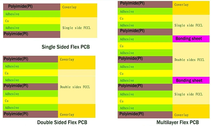
Single-Layer Flex PCB:
A single-layer flex PCB comprises a single conductive layer, usually copper, positioned between two flexible polymer layers, commonly made of polyimide. This conductive partition furnishes the mandated traces and pad areas for component coupling. This type of flex PCB is suitable for simpler designs with relatively low complexity, or when bending in a single direction is required.
Double-Layer Flex PCB:
Double-layer flex PCB consist of two conductive layers separated by an insulating layer. Usually composed of copper, the conductive layers are connected through plated through-holes . The insulating layer can be a flexible material like polyimide or a rigid material such as FR-4. The top and bottom layers may have separate circuitry or be interconnected through vias. Double-layer flex PCB offer increased design flexibility, allowing for more intricate circuit layouts and the option to accommodate components on both sides.
Multi-layer Flex PCB:
Multi-layer flex PCB incorporate three or more conductive layers, with insulating layers in between. The synergy within the conductive layers is achieved via a conglomerate of PTHs and vias. Insulating substrates could intermingle flexible and rigid materials, selected predicated on design requisites. Multi-layer flex PCB provide the highest degree of complexity and functionality, enabling dense circuitry, multiple component mounting options, and advanced signal routing. Such PCB are prevalently seen in applications where spatial economy is vital, such as in smartphones, tablets and wearables.
It’s important to recognize that the specific construction of flex PCB can vary depending on factors such as the manufacturer, design specifications, and application. The number of layers, materials utilized, and fabrication techniques employed may differ. Nevertheless, the previously mentioned tenets disseminate a rudimentary comprehension of the usual fabrications pertaining to single layer, double sided and multilayer flexible PCB.
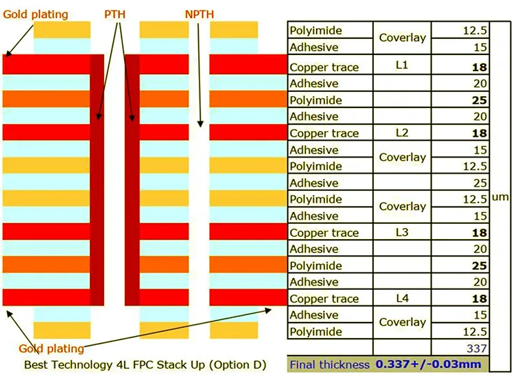
Multilayer Flex PCB Stack-up
Here is stack up of a normal 4-layer flexible circuit:
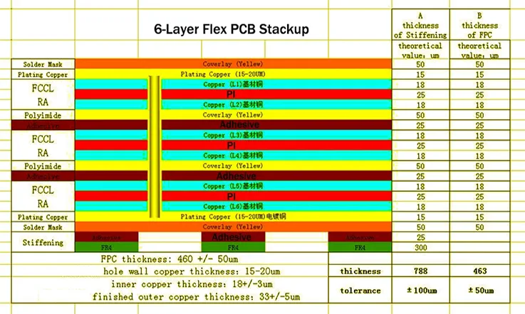
The proposed design is a 6-layer flexible circuit that incorporates an FR4 material stiffener in its stack-up. The Hole Wall Copper thickness measures between 15-20 micrometers. The customer’s specified impedance value is approximately 90 Ohms with a tolerance of +/-10%.
Types of Multilayer Flex PCB
Flexible Copper Clad Laminate (FCCL) is a crucial component used in the fabrication of flexible PCB, including rigid-flex PCB. It consists of alternating layers of copper foil and polyimide or polyester. The choice of copper foil and PI directly affects key attributes of multi-layer flex PCB, including thickness and flexibility.
There are two main categories of FCCL based on the PI used: glued and adhesive-free multilayer flex PCB. Additionally, different types of copper foils, namely Rolled Annealed (RA) copper and Electrodeposited (ED) copper, are used in FCCL for multilayer flex PCB.
Glued multilayer flex PCB:
Glued multilayer flex PCB are manufactured by bonding copper foil and adhesive-coated PI films. However, the adhesive employed in this process exhibits limitations in terms of heat resistance, dimensional stability, and chemical resistance. These PCB cannot endure temperatures above 200°C, and their tear strength significantly decreases at temperatures of 120°C or higher.
Consequently, glued FCCL is unsuitable for rigid-flex PCB, which often undergo lamination temperatures exceeding 200°C. These adhesive-based FCCLs are primarily used in flexible PCB operating at temperatures below 200°C.
Adhesive-free Multilayer flex PCB:
Adhesive-free FCCL can be produced in two ways. The first method involves using a PI film as the carrier and coating copper foil onto its surface. The second technique utilizes copper foil as the carrier, with liquid PI applied to its surface and subsequently cured. Adhesive-free multilayer flex PCB exhibit minimal dimensional changes even at high temperatures. At 300°C, the dimensional change rate remains within 0.1%. The exceptional dimensional stability of adhesive-free multilayer flex PCB enables fine lines to be achieved.
This is of particular importance in high-end electronic products like LCDs, PDPs and COF boards that require fine lines, high density, dimensional stability, and high-temperature resistance. Consequently, adhesive-free multilayer flex PCB are increasingly preferred. For example, JarnisTech offers adhesive-free multilayer flex PCB with a minimum trace width/space of 1.6mil/1.6mil.
Copper foil options in FCCL: FCCL for multilayer flex PCB employs two types of copper foil: Rolled Annealed (RA) copper and Electrodeposited (ED) copper.
RA copper multilayer flex PCB:
RA copper is obtained by heat and rolling processes to achieve the required thickness on FCCL. RA copper exhibits excellent resistance to bending, making it suitable for rigid-flex PCB and flexible PCB subjected to frequent movement. The price of RA copper multilayer flex PCB increases as the copper thickness decreases (below 0.5oz). The surface of RA copper foil is smooth, typically allowing circuit generation through laser technology. JarnisTech offers RA copper flex PCB with a minimum copper thickness of 25μm.
ED copper multilayer flex PCB:
ED copper is applied to FCCL through physical sputtering or electroplating processes, based on the desired thickness. The price of ED copper FCCL increases with higher copper thickness. JarnisTech provides ED copper multilayer flex PCB with a maximum copper thickness of 3oz. Although ED copper is less resistant to bending, it facilitates easier etching. Consequently, ED copper multilayer flex PCB are primarily used in static applications, such as connecting circuits and transmitting signals in lithium battery system covers, LED light PCB beauty masks, and various automotive lights (e.g., walling lights, door lights, position lights, marker lights).
Comparing Multi-layer Flexible PCB and Multi-layer Rigid PCB
Multi-layer Flexible PCB and Multi-layer Rigid PCB are both types of printed circuit boards used in electronic devices. Here’s a comparison between the two:
Flexibility: Multilayer Flexible PCB confer a key attribute of pliability, empowering them to flex, modify and adjust to varied geometries or reside within narrow confines. In juxtaposition, Rigid PCB possess an inherent rigidity, denying them the capability to cannot be bent.
Design: Flexible PCBs are optimally adaptable for design confronted with spatial limitations or intricate shapes. They bear the capacity to be folded, contorted, or wound to fit particular design parameters. On the contrary, Rigid PCB are better for designs that require a solid and stable structure.
Weight and Size: Flex PCB are generally lighter and thinner compared to their rigid counterparts. Their reduced weight and size make them ideal for lightweight and portable devices.
Durability: Rigid PCB typically demonstrate superior durability and imperviousness to impairment, insusceptible as they are to any forms of bending or flexing. While Flexible PCBs can endure a certain extent of bending and torsion, their susceptibility but may be more prone to wear and tear.
Cost: In general, rigid PCB are more cost-effective due to their simpler manufacturing processes and widespread use. Flexible PCB involve additional manufacturing steps and specialized materials, making them relatively more expensive.
Assembly: Rigid PCB are typically easier to assemble due to their rigid structure, which provides stability during the soldering process. Flexible PCB may require specialized assembly techniques to ensure proper alignment and connection of components.
Both types of PCB have their own advantages and are suitable for specific applications. The selection among them is contingent on the exclusive prerequisites of the electronic apparatus, encompassing aspects like dimensional constraints, flexibility demands, and budgetary assessments.
Design Considerations for Multi layer Flex PCB
Designing a multilayer flexible PCB summons meticulous attention to diverse parameters to secure peak functioning and dependability. A few crucial design contemplations to register include:
Layer Stack-up:
The layer stack-up is a critical aspect of multi-layer flex PCB design. It determines the number of layers, layer thickness and material selection. The objective is to strike a balance between flexibility, durability and functionality. The stack-up must be optimized to minimize stress on the flex circuit during bending and ensure proper signal integrity.
Trace Routing:
Precise trace routing is vital to maintain signal integrity and prevent crosstalk in a multilayer flex PCB. Close attention should be paid to trace width, spacing, and impedance to ensure reliable signal transmission. It is important to avoid sharp bends or acute angles in trace routing since this can induce stress on the flex circuit and lead to failures.
Component Placement:
Thoughtful component placement is crucial when designing a multilayer flex PCB to accommodate the circuit’s bending and folding requirements. Components should be situated in areas where they won’t impede the movement of the flex circuit. Secure mounting of components is imperative to prevent damage during flexing.
Material Selection:
Choosing suitable materials for a multilayer flex PCB is critical for achieving optimal performance and reliability. Materials must be selected based on their ability to withstand bending and flexing without cracking or breaking. Thermal and electrical properties should also be considered to ensure proper signal transmission and effective heat dissipation.
Manufacturing Difficulties of Multi-layer Flexible PCB
Flexible Printed Circuit Boards are becoming increasingly popular due to their adaptability and space-saving features. Conversely, the fabrication route of multi-layer Flexible PCB is intricate and can confront numerous challenges. Presented here are some regularly encountered challenges in the production of multi-layer Flexible PCB:
1. Material Handling: Delicate materials such as polyimide, used in flexible PCB, can be easily compromised during the fabrication process. This necessitates specialized handling and storage protocols to avoid any potential damage.
2. Alignment: Multi-layer PCB require precise alignment of each layer. This is more challenging with flexible PCB because they can bend and distort, which can lead to misalignment.
3. Lamination: The lamination process requires high temperatures and pressure, both of which can potentially damage the flexible materials. It is crucial to carefully control over these conditions is essential to preclude distortion or layer separation.
4.Drilling and Plating: Drilling holes for vias on flexible PCB can be difficult due to the material’s softness. The plating process can also be challenging because of the need to ensure a uniform copper layer.
5. Soldering: Flexible PCB exhibit a higher vulnerability to thermal damage during the soldering operation. Excessive heat can prompt the materials to warp or distort, subsequently impacting the all-encompassing performance of the circuit board.
6. Circuit Design: Flexible PCB often find application in domains demanding intricate, 3D circuit designs. This can make the design and manufacturing process more challenging.
7. Cost: The materials employed for flex PCB, such as polyimide, carry a heavier price tag compared to those chosen for rigid PCB. The complexity of the manufacturing process further escalates the comprehensive cost.
8. Testing and Inspection: Testing flexible PCB can be challenging due to the potential for damage during handling.The pliability of the PCB can also render certain testing methods, like automated optical inspection, more arduous.
To overcome these challenges, manufacturers often need to use specialized equipment and techniques. They must also invest in training their staff to handle flex PCB materials properly. Despite these difficulties, the advantages of flex PCB, like their lightness, flexibility and ability to fit into small or awkward spaces, and make them an attractive option for many applications.
When to Use Multilayer Flexible PCB?
The Multilayer Flexible PCB board finds its suitability in various applications due to its distinct advantages and capabilities. Here are some specific areas where this type of PCB is often utilized:
Ground and Power Plane Applications:
Multi layer Flex PCB are well-suited for incorporating ground and power planes, which provide stable and efficient power distribution throughout the circuit. The flexibility of the board enables it to adapt to different shapes and fit into confined spaces, making it an excellent choice for these applications.
Shielding Applications:
The flexibility of Multi-layer Flexible PCB allows them to be effectively utilized for shielding applications. They can be designed to provide shielding and EMI/RFI protection, ensuring proper isolation and minimizing electromagnetic interference.
High Circuit Density:
When the circuit density and layout requirements exceed the limitations of a single-layer PCB, Multi-layer Flexible PCB become an ideal solution. The additional layers allow for increased routing options and interconnected complexity, accommodating intricate designs with high component density.
Controlled Impedance with Shielding:
Multi layer Flexible PCB can be designed with controlled impedance characteristics while incorporating shielding layers. This combination enables reliable signal transmission while minimizing signal distortion and external interference.
Increased Circuit Density:
Applications that demand compact form factors and increased circuit density can benefit from Multi layer Flexible PCB. Their ability to stack multiple layers of circuitry in a flexible format allows for space-efficient designs without compromising functionality.
Crosstalk Elimination:
Multi layer Flexible PCB offer the advantage of reducing crosstalk between traces. With careful design considerations, such as controlled spacing and proper layer arrangement, they can minimize signal coupling and ensure signal integrity.
These applications highlight the versatility of Multi layer Flexible PCB, but their potential usage extends beyond these examples. For a comprehensive understanding of how this board can meet your specific requirements, we recommend contacting us to explore further possibilities and specifications.
How to Choose A Multi-layer Flexible PCB Manufacturer?
Selecting for a dependable and appropriately fitted manufacturer for multilayer flexible PCB is fundamental to guarantee the superior quality, efficiency and prompt delivery of your electronic commodities. Below are some key factors to consider when picking a multilayer flexible PCB producer:
Experience and Expertise:
Find a manufacturer boasting demonstrable success and substantial proficiency in producing multilayer flexible PCB. Scrutinize their professional background, the longevity of their operation, and their specialization in crafting superior-quality flexible PCB.
Quality Standards and Certifications:
It is critical to ensure that the manufacturer adheres to stringent quality control procedures and possesses pertinent endorsements, such as ISO 9001 or ISO 13485. These accreditations reflect an unwavering dedication to uphold premium manufacturing standards.
Manufacturing Capabilities:
Assess the manufacturer’s manufacturing capabilities, including their equipment, facilities, and production capacity. Make sure they have the necessary resources to handle the complexity and volume of your multilayer flex PCB requirements.
Design and Engineering Support:
A reputable manufacturer should offer design and engineering support to assist you in optimizing your multilayer flexible PCB design. They should be able to review your design files, provide design for manufacturability (DFM) feedback, and offer technical expertise throughout the manufacturing process.
Material Selection:
Verify that the manufacturer uses high-quality materials suitable for multilayer flexible PCB. The choice of materials, including the flexible substrates and adhesives, can impact the performance and reliability of the finished PCB.
Production Lead Time and Flexibility:
Consider the manufacturer’s production lead time and their ability to accommodate your production schedule. Flexibility in terms of order quantity and quick turnaround times can be advantageous, especially if you require rapid prototyping or have changing production requirements.
Quality Assurance and Testing:
Inquire about the manufacturer’s quality assurance processes, including the testing and inspection methods they employ. They should conduct rigorous testing to ensure the reliability and functionality of the multilayer flexible PCB.
Cost and Pricing:
While cost should not be the sole factor, it’s important to consider the manufacturer’s pricing structure and whether it aligns with your budget. Request detailed quotations, including any additional costs for tooling, testing, or customized requirements.
Communication and Support:
Evaluate the manufacturer’s communication channels and responsiveness. Clear and open communication, along with responsive customer support, is crucial for addressing any concerns, providing updates and resolving issues throughout the manufacturing process.
By considering these factors and conducting thorough research, you can identify a multilayer flexible PCB manufacturer that meets your specific requirements and can deliver high-quality products within your timeline.
Conclusion
Multilayer flexible printed circuit boards offer distinct advantages that make them highly suitable for a wide array of electronic applications. In comparison to traditional rigid PCB, they provide superior flexibility, durability, and space efficiency.
The growing demand for smaller and more intricate devices has significantly contributed to the increasing popularity of multilayer flex PCB. These boards find ideal application in industries such as medical devices, aerospace, and military equipment, where space constraints are prevalent, and reliability is paramount.
To ensure an optimal design tailored to specific application requirements, it is crucial to collaborate with an experienced manufacturer like JarnisTech. Our expertise ensures that factors like the number of layers, choice of materials, and overall board size and shape are meticulously considered during the design process.
In conclusion, multilayer flex PCB are a compelling choice for creating electronic devices that prioritize high quality and reliability. Given their myriad advantages and growing prominence, they are poised to remain a vital component in the electronics industry for years to come.


