
The PCB industry remains committed to delivering products that offer exceptional performance and the lowest possible signal loss. A smooth copper foil layer represents one of the factors that contribute to the highest PCB board performance. Notably, in high-frequency PCB designs, different copper foil types having varying levels of surface roughness are utilized. Furthermore, the thickness of copper foil varies based on its intended application.
In this regard, it is essential to gain a more in-depth understanding of copper foil and how it is employed in the manufacturing of printed circuit boards (PCBs).
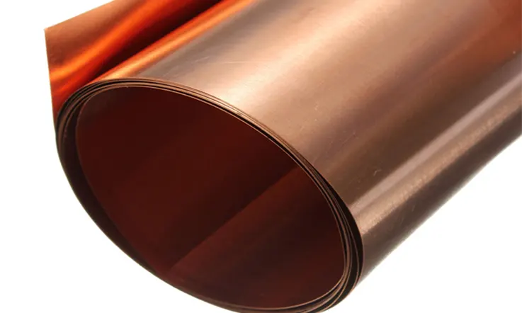
What Is Copper Foil in Printed Circuit Boards ?
Copper foil is a material exhibiting a negative electrolytic charge. It serves as a vital element in the production of printed circuit boards (PCBs), where it is deposited onto the base layer to create a continuous metal foil, also referred to as a conductor. Through a process of etching, copper foil can form a circuit pattern that may be printed with a protective layer, and bonded to the insulating layer with ease.
Copper foil is renowned for having a low surface oxygen rate and can be affixed to different substrates, such as metals and insulators. This material is most commonly used for electromagnetic shielding and antistatic applications. To achieve optimal continuity and exceptional electromagnetic shielding, the conductive copper foil is situated on the substrate surface and integrated with the metal substrate.
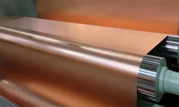
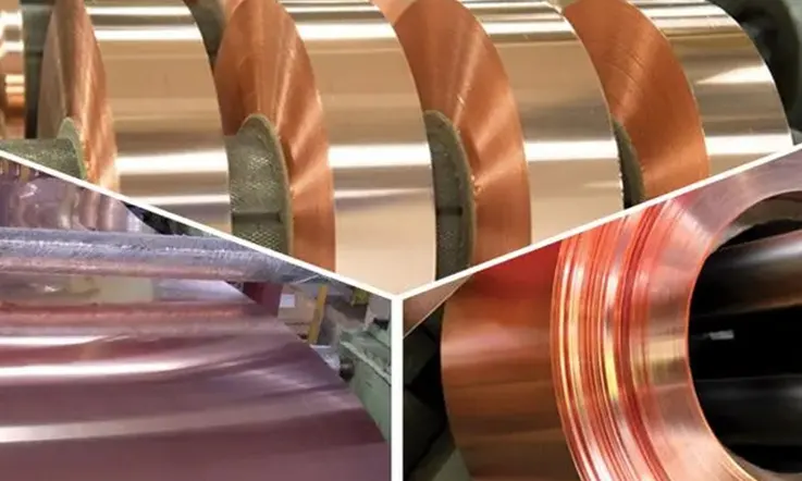
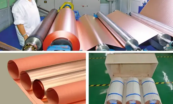
Manufacturing Process of PCB Copper Foil
Possible steps involved in the manufacturing process of PCB Copper Foil are:
● Preparation of Copper: The process starts with the preparation of high-quality copper cathodes, which are melted and cast into large slabs or plates. The copper may be refined and alloyed with small amounts of other elements, such as tin or zinc, to improve its properties.
● Rolling of Copper: The copper slabs are then rolled between high-speed rollers that progressively reduce the thickness of the metal while increasing its length and width. The rolling may be done hot or cold, depending on the desired mechanical properties and surface finish. The rolled copper is then annealed to relieve any stresses and improve its ductility.
● Surface Treatment: The copper foil is then subjected to various chemical and mechanical treatments to modify its surface properties and ensure good adhesion to the insulating substrate. These treatments may include cleaning, degreasing, roughening, etching, and coating with a thin layer of oxide or other protective material.
● Lamination of Copper Foil: The copper foil is then laminated onto the insulating substrate, which could be a rigid or flexible material such as FR-4, polyimide, or PET. The lamination may be done using adhesives, pressure, or heat, depending on the type of substrate and the bonding requirements.
● Chemical Treatment of Copper Foil: The copper foil is then etched using a chemical solution that removes the unwanted copper and creates the desired circuit pattern. The etchant may be a solution of ferric chloride, cupric chloride, or ammonium persulfate, depending on the characteristics of the copper foil and the substrate.
● Inspection and Quality Control: At various stages of the manufacturing process, the copper foil is subjected to quality control tests to ensure that it meets the desired specifications for thickness, width, tensile strength, conductivity, peel strength, and other properties. A final visual inspection may also be performed to detect any defects or deviations from the design.
● Storage and Transportation: Once the copper foil production process is complete and the product has passed quality control, the copper foil is then packaged, stored and transported to the customer. Proper storage and handling conditions are necessary to ensure that the copper foil retains its properties and does not get damaged or contaminated.
Properties of PCB Copper Foil
Some of the key properties of PCB copper foil are:
● Thickness: The thickness of copper foils used for PCB manufacturing can vary from a few microns to several tens of microns, depending on the application and the manufacturing process.
● Width: Copper foils used for PCB manufacturing typically come in rolls or sheets that can vary in width from a few centimeters to several meters, depending on the manufacturing process and the customer’s requirements.
● Tensile Strength: Copper foils used for PCB manufacturing have high tensile strength, which allows them to withstand mechanical stress and deformation during the manufacturing process and when in use.
● Conductivity: Copper foils used for PCB manufacturing are highly conductive, allowing them to efficiently transmit electrical signals and power between different components in the circuit board.
● Peel Strength: Copper foils used for PCB manufacturing have good peel strength, allowing them to adhere well to the substrate material. This is important for ensuring good electrical contact and mechanical stability between the copper foil and the substrate.
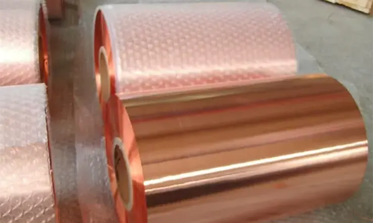
● Surface Finish: Copper foils used for PCB manufacturing can have various surface finishes, such as smooth, matte, or rough, depending on the manufacturing process and the customer’s requirements. The surface finish can affect the adhesion, solderability, and corrosion resistance of the copper foil.
● Thermal Conductivity: Copper foils used for PCB manufacturing have high thermal conductivity, which makes them effective at dissipating heat and reducing the risk of thermal damage to the components and the substrate.
As a result, the properties of copper foil used for PCB manufacturing are critical for ensuring the quality, reliability, and performance of the final circuit board.
Types of Copper Foil in PCB Fabrication
The proper transmission of signals along copper pathways is an essential aspect of the performance of Printed Circuit Boards (PCBs). Neglecting any element of the PCB design may lead to signal distortions.
Copper is a critical factor in PCB construction, as its type, quality, and ability to adhere to the PCB’s dielectric layer can make or break the assembly. Despite popular belief, copper used in PCBs is a complex material that requires careful attention.
Two forms of copper foils that are commonly used in the manufacture of Printed Circuit Boards (PCBs) are Electrodeposited (ED) and Rolled-Annealed (RA) Copper. It is imperative to gain an understanding of the properties of both types of copper foil to make informed decisions when selecting the appropriate copper foil for a specific PCB assembly.
Electrodeposited (ED) Copper Foil
Electrolytic copper (ED Copper) is manufactured by plating copper onto a drum. The thickness of the copper foil is regulated by the drum’s rotation speed, which means that thicker copper requires more time to plate. The side of copper that is adjacent to the drum has a smoother texture, while the opposite side has a more uneven texture, and the grain structure of the copper is perpendicular to the plane.
A defining characteristic of ED copper is that it has a vertical grain structure. However, when compared to Rolled-Annealed (RA) copper, standard ED copper’s surface tends to have a higher profile, resulting in a rougher surface. Therefore, the use of ED copper may not support excellent signal integrity and is less flexible.
Rolled-Annealed (RA) Copper
The production process of Rolled-Annealed (RA) Copper involves the passage of pure copper ingots through several rolling processes until the desired thickness is achieved. This process results in copper foil with a uniform surface roughness, with an average RMS (root mean square) value of 0.35 microns.
RA Copper enjoys widespread use in the fabrication of flex circuits and rigid-flex PCBs, owing to its grain structure and smooth surface, which are ideal for dynamic and flexible circuitry. The use of RA Copper is also advantageous for applications requiring high-frequency signal transmission, as surface roughness has been shown to impact high-frequency insertion loss, with a smoother copper surface being desirable.
Copper Foil Features
● In the construction of multilayer PCB boards, the copper utilized for the outer layers manifests in the form of copper foil, which is then incorporated by pressing it with the prepregs or cores. However, when using microvias on HDI PCB, the copper foil adheres directly to RCC (resin-coated copper).
● In the production of standard PCBs, the final copper thickness on inner layers is identical to the initial copper foil thickness. Additionally, during the panel plating process, up to 18-30μm of extra copper is added to the tracks on outer layers.
● The copper foils that are employed in the process of fabricating PCBs are of electronic grade with a purity of 99.7%, and they range in thickness from 1/3oz/ft² (12μm or 0.47mil) to 2oz/ft² (70μm or 2.8mil).
● Copper foil possesses a lesser quantity of surface oxygen and can be laminated manufacturers to various base materials – including but not limited to metal core, polyimide, FR-4, PTFE, and ceramic – in order to create copper-clad laminates. Furthermore, copper foil can also be introduced in a multilayer board before the pressing stage.
Thickness of Copper Foil
Copper foil is a crucial element in printed circuit board (PCB) design. It is the initial layer of copper applied to both the outer and inner layers of multilayer PCB boards. The thickness of the copper foil directly impacts the flow of charges within the PCB, with better conductivity achieved through thicker layers. However, thick layers of copper foil can pose a challenge during the etching process. The thickness of the copper foil is usually quantified in terms of an ounce, with one ounce of copper foil capable of covering one square foot of board area. Copper foils on single-sided and double-sided PCBs generally have a thickness of 1.4 mils or 35µm. The most commonly used thicknesses for copper foils in PCBs are 18µm, 35µm, 55µm, and 70µm. Differentiating PCBs based on their thickness relative to their area is a standard practice in the industry.
Thickness of Surface Conductor & Foil Plus Plating
The minimum overall thickness of the conductor, comprising copper foil and copper plating, must comply with the guidelines outlined in Table 3-1 of IPC-A-600G once the processing has been completed, except if explicitly stated otherwise in the procurement documents.
Table 3-1: External Conductor Thickness after Plating
| Weight | Absolute Cu Min. (IPC-4562 less 10% reduction) (μm) [μin] | Plus Min. Plating for Class 1, 2 (20μm) [787μin] | Plus Min. Plating for Class 3 (25μm) [984μin] | Max. Variable Processing Allowance Reduction* (μm) [μin] | Min. Surface Conductor Thickness after Processing (μm)[μin] | |
| Class 1, 2 | Class 3 | |||||
| 1/8oz | 4.60 [181] | 24.60 [967] | 29.6 [1,165] | 1.50 [59] | 23.1 [909] | 28.1 [1,106] |
| 1/4oz | 7.70 [303] | 27.70 [1,097] | 32.70 [1,287] | 1.50 [59] | 26.2 [1,031] | 31.2 [1,228] |
| 3/8oz | 10.80 [425] | 30.80 [1,213] | 35.80 [1,409] | 1.50 [59] | 29.3 [1,154] | 34.3 [1,350] |
| 1/2oz | 15.40 [606] | 35.40 [1,394] | 40.40 [1,591] | 2.00 [79] | 33.4 [1,315] | 38.4 [1,512] |
| 1oz | 30.90 [1,217] | 50.90 [2,004] | 55.90 [2,201] | 3.00 [118] | 47.9 [1,886] | 52.9 [2,083] |
| 2oz | 61.70 [2,429] | 81.70 [3,217] | 86.70 [3,413] | 3.00 [118] | 78.7 [3,098] | 83.7 [3,295] |
| 3oz | 92.60 [3,646] | 112.60 [4,433] | 117.60 [4,630] | 4.00 [157] | 108.6 [4,276] | 113.6 [4,472] |
Note:
According to the specifications, Cu plating thickness for Class 1 and Class 2 must be 20μm [787μin], while a thicker plating of 25μm [984μin] is required for Class 3. Moreover, due to the reduction in process allowance, rework procedures are not allowed for weights less than 1/2 ounce. However, for weights exceeding this mark, the reduction in process allowance permits a single rework operation to be carried out.
Thickness of Copper Foil: Internal Layers
The minimum thickness of copper foil, also referred to as the conductor thickness, is defined as the maximum thickness that can sustain a continuous flow of electrical current. In arriving at this value, individual scratches are taken into consideration but the “dendritic” surface that is used to facilitate metallic adhesion is not factored in, in order to provide an accurate determination of the minimum foil thickness.
After undergoing processing, it is essential that the minimum internal layer copper foil thickness conforms to the specifications specified in Table 3-2 of the IPC-A-600G.
Table 3-2: Internal Layer Foil Thickness after Processing
Weight (oz) [μm] | Absolute Cu Min. (IPC-4562 less 10% reduction) (μm) [μin] | Max. Variable Processing Allowance Reduction* (μm) [μin] | Min. Final Finish after Processing (μm)[μin] |
| 1/8 [5.10] | 4.60 [181] | 1.50 [59] | 3.1 [122] |
| 1/4 [8.50] | 7.70 [303] | 1.50 [59] | 6.2 [244] |
| 3/8 [12.00] | 10.80 [425] | 1.50 [59] | 9.3 [366] |
| 1/2 [17.10] | 15.40 [606] | 4.00 [157] | 11.4 [449] |
| 1 [34.30] | 30.90 [1.217] | 6.00 [236] | 24.9 [980] |
| 2 [68.60] | 61.70 [2,429] | 6.00 [236] | 55.7 [2,193] |
| 3 [102.9] | 92.60 [3,646] | 6.00 [236] | 86.6 [3,409] |
| 4 [137.20] | 123.50 [4,862] | 6.00 [236] | 117.5 [4,626] |
Above 4 [137.20] | – | 6.00 [236] | 6μm [236μin] below minimum thickness of calculated 10% reduction of foil thickness in IPC-4562 |
● Rework operations are not authorized for weights that are less than 1/2 ounce, owing to the reduction in process allowance. Conversely, for weights exceeding 1/2 ounce, the process allowance reduction permits a single rework procedure to be carried out.
● It is worth noting that in cases where additional plating might be essential for internal layer conductors, the plating thickness requirements must be distinctly specified as an independent plating thickness requirement.
Which Type of Copper is Best for Your PCB ?
When designing a printed circuit board (PCB), the selection of appropriate materials is crucial to ensure optimal performance and reliability of the circuit. For high-frequency applications, the type of copper foil, its surface roughness, and its adhesion to dielectric material are all critical factors that determine whether the PCB will perform at its fullest potential.
For very thin circuits, particularly those used in high-speed digital or millimeter wave applications, the surface roughness of the copper plays a significant role. The thinner the substrate, the more sensitive it is to surface roughness, and copper planes in close proximity have a significant impact on performance. As such, it is essential to select a copper foil with low surface roughness for high-frequency designs that require high precision etching.
In particular, for ultra-thin laminates, the surface roughness of the copper foil can significantly impact performance. Therefore, it is essential to choose a copper foil with a smoother surface to ensure high accuracy etching in support of very high-frequency applications.
So, choosing the right copper foil with a smooth surface and strong adhesion to dielectric material is a critical decision in designing high-frequency PCBs. It is also advisable to consider the effects of surface roughness on circuit performance and strive to achieve high accuracy etching for delicate and sensitive designs that utilize thin materials.
| Feature | ED Copper Foil | RA Copper Foil |
| Appearance | Red | Yellowish |
| Surface roughness | The surface facing the solution is considerably more rough. | On both sides of the copper, the surface roughness is similar. Smoother than ED Copper. |
| Properties | Mechanically extremely sturdy. Fast thermal cycling can produce thermal stress fractures in ED copper-formed thin conductors. Greater tensile strength and elongation prior to rupture. As copper roughness grows, conductor loss and insertion loss will also increase. | High resistance to cracking due to thermal stress in situations where thermal shock may be a concern. Superior elongation elasticity prior to permanent deformation. Provides enhanced etch definition for high-frequency, fine-featured circuits. |
| Applications | Ideal for applications where mechanical stress is a consideration. | Suitable for high-frequency applications. |
What Does Copper Foiling Do in a PCB ?
Printed circuit boards (PCBs) consist of numerous layers and components, including traces, metal layers, silkscreen, and other materials, without which PCBs cannot function. Traces, which serve as the “blood arteries” of the PCB’s skeleton, are vital as no charge flow can occur without traces. In today’s world, PCBs are a critical component of virtually every electrical device.
Copper is the most critical component of printed circuit boards (PCBs) as it is primarily used to create traces. Due to its excellent conductivity, copper is widely used in PCBs as electrical impulses can travel quickly without being disrupted. Copper’s high conductivity is attributed to its valence shell containing a single electron, allowing it to readily travel from one atom to another without encountering any obstacles. Therefore, copper can effectively carry electric charges without causing any signal degradation.
In the first layer of PCBs, copper and a negative electrolyte are used to create a continuous metal foil. Copper is highly compatible with several substrates, metals, and insulating layers due to its low surface oxygen level. Copper is easily bonded with insulating layers on the PCB, and after etching, it can be used with the protective layer to create a wide range of circuit layouts. Copper foil also provides excellent continuity of electromagnetic shielding, making it ideal for use on the surface of the substrate sheet.
Copper Foil Selection
The selection of copper foil for a PCB design depends on several factors, including the desired copper thickness, copper purity, and the copper-dielectric interface profile.
For high-frequency applications, it is advisable to use low-profile copper, as it exhibits lower signal loss at high frequencies. This is because low-profile copper minimizes the interface between the copper and dielectric material, which can cause signal loss.
Copper thickness is another critical factor to consider when selecting copper foil. The typical thickness range is between 0.25 ounces (0.3 mils) to 5 ounces (7 mils). The thickness of the copper may vary based on the intended application. For instance, applications requiring a high amount of power ought to use significantly thicker copper layers.
Copper purity refers to the amount of copper present in a square meter of copper foil. Copper foil with an electronic grade purity level usually has a purity of around 99.7%. A high purity level ensures excellent electrical conductivity, providing top-notch performance in electronic circuits.
Applications of PCB Copper Foil
Possible applications of PCB copper foil include:
● Printed Circuit Boards (PCBs): Copper foil is widely used as a substrate and conductor in rigid PCBs, where it provides a stable and conductive surface for the attachment of electronic components such as resistors, capacitors, and integrated circuits.
● Flexible PCBs: Copper foil can also be used in flexible PCBs, where it enables the circuits to bend, twist, and conform to different shapes and sizes. Flexible PCBs are commonly used in applications such as mobile devices, wearable electronics, and automotive sensors.
● Radio Frequency (RF) Circuits: Copper foil is an essential component in RF circuits, where it is used to transmit and receive electromagnetic signals with minimal loss and interference. RF circuits are used in wireless devices, antennas, and communication systems.
● Energy Storage Systems: Copper foil is used in energy storage systems such as batteries and supercapacitors, where it forms the current collector that conducts electrons between the electrodes and terminals. Copper foil provides a high surface area that can enhance the energy density and performance of the system.
● LED Lighting: Copper foil is used in LED lighting applications, where it serves as a reflective layer that redirects the emitted light in a desired direction. Copper foil can also serve as a heat sink that dissipates the heat generated by the LED, which can enhance the reliability and lifetime of the device.
Importance of PCB Copper Foil
The importance of PCB copper foil lies in its crucial role in the construction and functioning of electronic devices, particularly those that use printed circuit boards. Below are some reasons why PCB copper foil is vital:
● Electrical Conductivity: Copper foil is a highly conductive metal that can efficiently transmit electrical signals between different components in a circuit board. This makes it an ideal choice for use as a conductor in PCBs.
● Strength and Durability: Copper foil is a relatively strong and durable material that can withstand thermal stress, mechanical deformation, and other environmental factors that can impact the performance of a circuit. This makes it ideal for use as a substrate and conductor in PCBs.
● Flexibility: Copper foil is also highly flexible and can easily conform to the shape of the circuit board or substrate. This makes it an ideal choice for use in flexible PCBs, which can be bent, twisted, or folded into different shapes.
● Cost-Effectiveness: Copper foil is a relatively inexpensive material that can be easily manufactured and processed. This makes it an attractive choice for use in mass-produced electronic devices that require reliable and affordable PCBs.
● Compatibility: Copper has good compatibility with a wide range of other materials and chemical treatments, which allows for seamless integration with different components in a circuit board. This makes it an ideal choice for use in various applications and industries such as telecommunications, automotive, aerospace, and medical devices.
In a word, the importance of PCB copper foil lies in its essential role in enabling the proper functioning and performance of electronic devices that are used in a range of industries and applications.
Future Trends and Challenges
Possible future trends and challenges related to PCB Copper Foil may include:
● Miniaturization: As electronic devices continue to get smaller and more complex, there is a growing demand for even thinner and more precise copper foils that can support high-density interconnects and fine-pitch components.
● Higher Frequencies: With the rise of 5G, IoT, and other wireless technologies, there is a need for copper foils that can handle higher frequencies and offer lower signal loss and impedance.
● Sustainability: The PCB industry is under pressure to reduce its environmental impact and reduce the use of toxic chemicals and waste. New methods of recycling and electroplating copper foils, as well as alternative materials, may become more prominent.
● Supply Chain Disruptions: The COVID-19 pandemic has highlighted the vulnerability of global supply chains, and disruptions in the availability and cost of raw materials, labor, and logistics can affect the production and price of copper foils.
● Standards and Regulations: The PCB industry is subject to various national and international standards and regulations that govern the use and disposal of copper foils. Compliance with these standards may require additional testing, documentation, and reporting, which can increase costs and affect market access.
● Intellectual Property: The development of new copper foil technologies and processes may involve collaborations, licensing, and patent disputes. Companies may need to invest in R&D, legal strategies, and market differentiation to protect their competitive advantage.
Summary
JarnisTech Is a One-Stop Service PCB manufacturing and Assembly Factory in China
As a leading provider of PCB solutions, JarnisTech understands the importance of meeting specific copper thickness requirements in today’s ever-changing market. To this end, we offer a wide selection of copper foils from world-renowned suppliers, such as Denkai America, JX Nippon Mining & Metals Corp, Mitsui Kinzoku, and Wieland, that are compatible with a diverse range of standard and application-specific PCB designs.
Our copper foils are specially crafted to meet the high demands of HDI, HSD, and MSAP designs, ensuring superior adhesion and signal integrity. We offer a broad range of copper weights, ranging from 12m (1/3oz) to 210m (4oz), allowing us to cater to the varying copper thickness needs of our clients, particularly for thick copper PCBs.
With over two decades of experience in the PCB industry, JarnisTech provides an extensive range of PCB services, including rigid-flex, rigid PCB, flexible printed circuit board, copper foil, and many others. Moreover, we offer comprehensive turn-key solutions for PCB manufacturing and assembly, enabling our clients to benefit from seamless development and fabrication processes.
Related Posts:
1. Selecting PCB Laminate Materials: A Comprehensive Overview
2. PCB Copper Trace Width and Space: Everything You Need to Know About Them
3. Which Types are Most Commonly Used in PCB Substrates?
4. What Is Fiberglass PCB and Why Fiberglass Used in PCB Manufacturing?
5. Standard PCB Thickness-Choosing the Correct Thickness for PCB


