
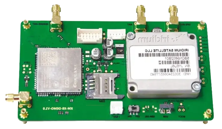
In today’s interconnected world, the telecommunications sector is experiencing rapid advancements, driven by the demand for faster and more reliable communication technologies. At the heart of these innovations lies a critical component: the Printed Circuit Board (PCB). The design, manufacturing, and assembly of telecommunications PCBs are pivotal processes that support the performance of high-speed and high-frequency communication systems. This article explores the intricate world of telecommunications PCBs, providing insights into design considerations, manufacturing processes, and the this dynamic industry.
Design Considerations for Telecommunications PCBs
1. Advanced Multilayer Telecommunications PCBs for High-Speed Communication
Understanding Multilayer Design Principles-
Multilayer PCBs are integral to the advancement of telecommunications technology. These boards comprise multiple layers of conductive pathways, enabling complex routing of electrical signals while maintaining a compact design. This layered structure optimizes real estate on the board, making it possible to fit an increasing number of circuits and components within a limited area. By strategically layering materials, designers can enhance signal integrity and reduce the adverse effects of signal loss and crosstalk. For instance, a 4-layer PCB might be sufficient for a simple communication device, while more advanced applications—like 5G technology—often require 6 or more layers to accommodate additional circuitry and improved signal routing.
Benefits of Layer Stacking in High-Speed Applications-
The practice of layer stacking allows for a denser arrangement of circuits, which is especially beneficial in telecommunications, where space constraints are common. By carefully planning the stack-up of layers, engineers can significantly improve the electrical performance of PCBs. Each layer can serve a specific purpose: for example, one layer might be dedicated to power distribution, while another handles signal ground, which minimizes noise and enhances reliability.
Consider the typical stack-up for a high-speed telecommunications PCB, which might look like this:
| Layer | Function |
| 1 | Signal Layer |
| 2 | Ground Plane |
| 3 | Power Distribution Layer |
| 4 | Signal Layer |
This organization promotes effective power management and signal integrity for devices that operate at high frequencies. Thoughtful layer stacking improves thermal performance by evenly distributing heat across the PCB, which benefits high-performance telecommunications systems. These strategies not only enhance device performance but also extend their lifespan, ensuring reliability in demanding environments.
Trade-offs Between Complexity and Performance-
While multilayer designs offer significant benefits, they come with inherent complexities. Each additional layer increases manufacturing costs and can complicate assembly processes. For instance, the more layers present, the more meticulous the design and manufacturing tolerances must be. Designers face challenges in ensuring that vias and traces are correctly aligned and that layers are bonded effectively without introducing defects.
The increased complexity may also complicate troubleshooting and repairs. In some cases, a multilayer PCB can resemble a labyrinth, making it challenging to pinpoint issues without advanced diagnostic tools. Therefore, engineers must evaluate the trade-offs between desired performance levels and practical production considerations. A clear understanding of the project’s goals and the capabilities of the manufacturing process can guide these decisions. For example, while a 10-layer PCB might offer unparalleled performance, a simpler 4-layer design may be sufficient for certain applications without straining the budget or production timeline.
2. RF and High-Frequency Design in Telecommunications PCBs
Key Factors for RF Signal Integrity-
For effective RF design in telecommunications PCBs, maintaining strong signal integrity is a priority. High-frequency RF signals can easily be affected by factors like impedance mismatches and dielectric losses, which degrade signal quality. Design strategies must include careful layout to keep impedance uniform across the PCB. Using controlled impedance traces helps preserve signal quality and minimize reflections, which can otherwise compromise the signal. Additionally, choosing dielectric materials with low-loss properties supports robust signal transmission, especially in high-frequency scenarios, ensuring clear and reliable performance.
Incorporating RF design guidelines, like proper trace width calculations and spacing, can greatly improve performance. This meticulous approach to RF signal integrity helps to prevent unwanted interference, ultimately ensuring that telecommunications devices perform reliably.
Techniques for Minimizing Transmission Loss-
Transmission loss is the enemy of effective communication. It can significantly degrade the quality of RF signals as they traverse the PCB. To combat this, engineers employ a variety of strategies. One effective technique is minimizing trace lengths—shorter traces reduce the potential for loss and delay. Think of it as taking the most direct route; the fewer obstacles, the better!
Optimizing trace widths is another vital technique. Wider traces can handle higher currents with lower resistance, which translates into less heat and improved signal strength. Implementing solid ground planes is also a game plan that works wonders; they provide a low-resistance return path for signals, further minimizing loss. Here’s a quick summary of effective techniques to reduce transmission loss:
| Technique | Description |
| Shorter Trace Lengths | Reduces distance signals must travel |
| Optimized Trace Widths | Enhances current capacity and minimizes heat |
| Ground Planes | Provides a solid return path for signals |
Utilizing RF Simulation Tools for Design Accuracy-
With technological advances, RF simulation tools have transformed the PCB design landscape. These tools let engineers test and refine their designs virtually, catching potential issues well before manufacturing. Picture it like a practice run before the real thing—RF simulation provides a way to troubleshoot, optimize, and ensure everything works as planned. By modeling components and signal behavior, designers get a preview of how the final product will perform, saving time, cutting costs, and ensuring a smoother transition from concept to production. Give it a whirl and watch your designs come to life!
Simulation software can help identify potential issues, such as signal integrity problems or impedance mismatches, early in the design process. By making necessary adjustments based on simulation results, designers can avoid costly revisions and rework. Furthermore, these tools provide visual representations of how signals will behave on the PCB, offering invaluable insights into potential performance bottlenecks.
For example, a designer can simulate the effects of different dielectric materials or trace configurations on signal propagation, allowing for data-driven decisions that enhance overall design accuracy.
3. Custom Telecommunications PCB Layouts for Specific Needs
Tailoring Layouts for Specific Communication Standards-
In the realm of telecommunications, adhering to specific standards is a must. Various standards, such as those set by the Institute of Electrical and Electronics Engineers (IEEE), govern the design and performance of communication systems. When creating custom PCB layouts, it’s essential to align with these guidelines to ensure compatibility with existing technologies and components. This might include specific requirements for signal integrity, electromagnetic compatibility (EMC), and safety regulations.
For example, when designing a PCB for a device that must comply with IEEE 802.11 (Wi-Fi), the layout needs to facilitate high-speed data transmission while minimizing interference. Engineers often leverage industry-standard practices and tools to verify that their designs will meet these rigorous standards before moving into production.
Best Practices for Component Placement-
Thoughtful component placement is at the heart of effective PCB design. When placing components on a telecommunications PCB, designers must consider factors such as signal flow, potential interference, and thermal management. Placing high-frequency components close to each other can help maintain signal integrity, while grouping power components can improve thermal performance.
Here are some best practices for component placement:
| Best Practice | Description |
| Group Similar Components | Minimizes signal interference and enhances routing efficiency |
| Prioritize Critical Signals | Place critical components closer to the power supply and ground |
| Optimize Heat Dissipation | Position heat-sensitive components away from high-power areas |
Balancing Design Flexibility with Performance-
Flexibility in PCB design opens doors to innovation, but it also brings a unique set of challenges. Engineers must carefully evaluate whether the advantages of a flexible layout outweigh potential performance drawbacks. For instance, while a modular design can allow for future upgrades or changes, it might introduce additional complexity that can affect signal integrity or thermal management.
In designing telecommunications systems, balancing flexibility with performance often requires detailed simulations and careful analysis. For projects needing frequent updates, a modular approach supports adaptability and growth. On the other hand, applications demanding consistent output may benefit from a more structured design that focuses on stable performance. By customizing the approach—whether modular or fixed—designers can ensure the system aligns well with its intended use and delivers the reliability or versatility expected. Embracing these strategies means solutions can be both robust and ready for the long haul.
4. Signal Integrity and Impedance Control in Telecommunications PCB Design
Importance of Impedance Matching in PCB Design-
Impedance matching stands as a cornerstone in the design of telecommunications PCBs, especially for high-speed applications. When the impedance is not matched, signals can reflect back, causing disruptions that may lead to data loss or corrupted communication. To ensure seamless signal transmission, designers strive for uniform impedance throughout the board. This requires a thorough understanding of how different materials and geometries impact impedance.
For instance, using a specific dielectric material with known properties can help maintain consistent impedance. Similarly, the trace width and spacing must be meticulously calculated to achieve the desired impedance levels. The following table summarizes common materials and their dielectric constants, which influence impedance:
| Material | Dielectric Constant (εr) | Typical Use |
| FR-4 | 4.5 | General purpose PCBs |
| Rogers 4350B | 3.48 | High-frequency applications |
| PTFE | 2.1 | Microwave and RF circuits |
Strategies for Improving Signal Integrity-
Achieving high signal integrity involves implementing several strategic approaches. One effective technique is differential signaling, which transmits signals over two complementary lines. This method helps to cancel out noise and interference, ensuring that the receiving end receives a clear signal. Moreover, careful placement and routing of vias can further minimize disruptions.
For example, for 5G PCB designs, maintaining signal fidelity often means keeping trace lengths short and minimizing vias to reduce signal loss. Engineers rely on advanced simulation tools to visualize and refine the signal paths, examining how different layout decisions impact integrity. This way, they can make precise, data-backed adjustments, which is especially useful when working at high frequencies where even small layout choices make a difference. It’s like having a preview of performance, letting engineers fine-tune each detail before manufacturing begins.
Here’s a quick list of strategies for enhancing signal integrity:
●Differential Signaling: Reduce common-mode noise by sending signals as complementary pairs.
●Minimize Trace Lengths: Shorter traces lead to lower inductance and capacitance, reducing potential signal degradation.
●Optimize Via Usage: Limit the number of vias to prevent unnecessary signal loss.
Common Impedance Control Techniques-
To maintain impedance control throughout the PCB design, engineers have several techniques at their disposal. Adjusting trace widths is one of the most straightforward methods; wider traces lower impedance, while narrower traces increase it. Selecting the right dielectric material is another critical factor, as different materials have unique dielectric constants affecting signal behavior.
Controlled impedance structures are commonly used to ensure a stable impedance level regardless of environmental conditions, making them a reliable choice in high-frequency applications where variations can affect performance. By carefully designing these structures, engineers keep signal paths consistent, which helps to reduce issues like signal reflections or data loss. This approach provides a practical way to support high-speed signals and maintain signal integrity even in demanding settings, ensuring smooth operation and dependable connectivity in advanced telecom setups.
Incorporating these techniques from the design phase ensures optimal performance in telecommunications applications, ultimately enhancing the user experience.
5. Thermal Management and Durability in High-Frequency Telecommunications PCBs
Identifying Heat Sources in PCB Design-
Heat generation is a common challenge in electronic circuit operation, particularly in high-frequency telecommunications PCBs. It’s crucial to pinpoint potential heat sources right from the design stage. Common culprits include power components, voltage regulators, and high-frequency circuits, which can generate significant heat during operation.
Understanding where heat is generated allows engineers to take proactive steps in thermal management. For example, during the design phase, using thermal simulation tools can help visualize heat flow and identify hotspots before fabrication. This foresight can prevent issues down the road, ensuring your telecommunications PCB performs at its best.
Effective Thermal Management Solutions-
To tackle overheating in telecom PCBs, engineers use specific thermal management techniques that address high operational demands. A few common strategies include:
●Heat Sinks: These passive devices absorb and dissipate heat from components, effectively lowering their operating temperature. By increasing the surface area in contact with the air, heat sinks help ensure that power components remain cool under load.
●Thermal Vias: Integrating thermal vias into the PCB design allows heat to be conducted away from components to layers that can disperse heat more effectively. This technique is particularly useful in multilayer designs where heat can be routed to larger copper areas.
●Thermal Interface Materials (TIMs): Using high-performance TIMs between components and heat sinks can improve heat transfer. These materials fill microscopic gaps, ensuring better thermal contact and enhancing cooling efficiency.
Materials and Coatings for Enhanced Durability-
In telecom PCBs, the choice of materials and coatings directly impacts durability and resilience. High-performance options are specifically engineered to handle environmental stressors, such as rapid temperature changes and moisture, which can otherwise cause early breakdowns. With the right materials, PCBs can better withstand thermal cycling and resist degradation over time, even under demanding conditions. This careful selection of materials and coatings ensures that telecommunications equipment remains operationally reliable, providing consistent performance where it counts.
For example, materials like polyimide and thermally conductive ceramics are ideal for high-frequency applications due to their excellent thermal properties. Additionally, applying conformal coatings can protect PCBs from moisture, dust, and other environmental factors, extending their lifespan and maintaining performance.
Here’s a comparison of common PCB materials and their characteristics:
| Material | Temperature Tolerance | Moisture Resistance | Applications |
| FR-4 | Up to 130°C | Moderate | General-purpose PCBs |
| Rogers 5880 | Up to 200°C | High | RF and microwave circuits |
| Polyimide | Up to 260°C | Excellent | Flexible circuits and high-temp applications |
6. High-Speed Layout Rules for Telecommunications PCBs
Design Rules for Minimizing Electromagnetic Interference-
Electromagnetic interference (EMI) presents a serious challenge in the design of telecommunications PCBs. To tackle this issue, engineers must implement robust design rules that prioritize EMI mitigation. Here are some practical strategies:
●Trace Spacing: Ensure that traces carrying different signals are spaced appropriately to minimize coupling and interference. A general rule of thumb is to keep at least three times the width of the trace between signal traces to reduce the potential for crosstalk.
●Grounding Techniques: Using a solid ground plane can help shield sensitive components from EMI. Moreover, implementing star grounding techniques can reduce ground loops and ensure that return paths are as short as possible.
●Use of Ferrite Beads: Incorporating ferrite beads on power and signal lines can effectively filter out high-frequency noise, protecting sensitive areas of the PCB from unwanted EMI.
Guidelines for Routing High-Speed Signals-
When routing high-speed signals on telecommunications PCBs, certain best practices must be followed to maintain signal integrity:
●Short Signal Paths: Strive to keep signal paths as short as possible. Longer traces can introduce additional inductance and resistance, which can degrade the signal quality over time.
●Avoid Sharp Angles: Routing traces with gentle curves rather than sharp angles helps minimize inductance and maintain signal fidelity. For instance, a 45-degree bend is preferable to a 90-degree angle.
●Differential Pair Routing: When dealing with differential signals, ensure that pairs are routed closely together. This practice helps maintain a constant impedance and improves noise immunity.
The Role of Ground Planes in High-Speed Designs-
Ground planes serve a fundamental function in high-speed PCB designs, especially in telecommunications applications. Here’s how they contribute to effective signal management:
●Low-Impedance Path: A continuous ground plane offers a stable, low-resistance pathway for return currents, minimizing voltage inconsistencies and bolstering signal clarity. This layout is especially beneficial for high-frequency signals, where even slight fluctuations in ground potential can disrupt performance. The consistent grounding helps maintain signal integrity, enhancing reliability for demanding applications.
●Noise Reduction: Ground planes add a shielding layer that helps block out high-frequency noise, effectively protecting sensitive circuits and keeping communication signals clean. By creating this separation, ground planes reduce interference, which means less noise messing with your signal. For high-frequency designs, this isolation is like a guardrail that keeps signal quality consistent and smooth. It’s the kind of foundation that supports clearer communication without unwanted electronic “chatter” getting in the way.
●Thermal Management: Ground planes can also assist in thermal management by dispersing heat generated by components, which helps maintain performance and reliability over time.
7. Material Selection for High-Frequency Telecommunications PCB Performance
Overview of Common Materials Used in Telecom PCBs-
In telecommunications PCB design, choosing the right materials is a big deal for performance, especially when working with high frequencies. Different materials bring unique characteristics that directly impact functionality. For instance, low-loss dielectrics are often used for their ability to minimize signal degradation, while PTFE (polytetrafluoroethylene) materials are popular for their stability under varying temperatures. Some materials are more resistant to moisture, which is handy for environments prone to humidity. Here’s a snapshot of commonly used options and their perks for telecom applications:
●FR-4: This is the most widely used material due to its cost-effectiveness and decent performance at moderate frequencies. However, it may not be suitable for high-frequency applications due to higher dielectric losses.
●Rogers Materials: Often chosen for high-frequency applications, Rogers materials, such as RO4350B and RO4003C, feature low loss tangents and high thermal stability. These attributes make them ideal for RF and microwave designs, especially as signal frequencies rise.
●Teflon: Known for its excellent dielectric properties, Teflon is a top contender for high-frequency applications. Its low dielectric constant and loss factor contribute to minimal signal degradation, making it a preferred choice in advanced communication systems.
Low-Loss Dielectric Materials for 5G Applications-
With the rollout of 5G technology, the demand for low-loss dielectric materials has skyrocketed. Here’s what to consider:
●Material Characteristics: Low-loss materials are designed to transmit signals efficiently, minimizing attenuation and helping maintain signal integrity. This capability supports the high data rates and rapid response times that modern 5G networks demand. By utilizing these materials, engineers can enhance communication system performance, ensuring seamless data flow and optimal functionality. In today’s tech landscape, low-loss materials are a key factor in achieving reliable connectivity and efficient operations, making them a must-have for anyone looking to stay ahead in telecommunications.
●Examples of Low-Loss Dielectrics: Materials like Rogers 5880 and Isola’s I-Tera are specifically engineered for low-loss performance at high frequencies. Engineers should evaluate their specifications in relation to the expected operational frequencies to ensure optimal performance.
●Applications: Consider a telecommunications company developing a 5G base station. Utilizing a low-loss dielectric can reduce the amount of signal boosting needed, which translates to lower energy consumption and reduced operational costs.
Evaluating Cost vs. Performance in Material Choices-
Selecting materials for telecommunications PCBs involves weighing cost against performance. Here are some strategies:
●Cost Considerations: While high-performance materials offer superior electrical characteristics, they can also come with a hefty price tag. Engineers need to assess the long-term benefits against the upfront costs to determine the best option for their project.
●Performance Metrics: It’s important to establish clear performance metrics that align with the specific application. For example, if a project prioritizes high-frequency performance, investing in advanced materials may be justified despite higher costs.
●Example Comparison: A side-by-side comparison table can illustrate the trade-offs. Below is a simplified version:
| Material Type | Dielectric Constant | Loss Tangent | Cost per Square Foot |
| FR-4 | 4.5 | 0.02 | $2 |
| Rogers 4350B | 3.48 | 0.0037 | $15 |
| Teflon | 2.1 | 0.0002 | $25 |
8. Challenges in Signal Clarity and Noise Reduction for Telecommunications PCBs
Identifying Sources of Noise in PCB Designs-
Noise is a persistent challenge in the design of telecommunications PCBs, originating from various sources such as:
●Power Supplies: Fluctuations in power can introduce noise that interferes with signal clarity. Power supply designs must be robust, employing techniques like linear regulation and proper decoupling to minimize ripple.
●External Devices: Nearby electronics, like motors and RF transmitters, can introduce electromagnetic interference (EMI) that disrupts PCB performance. To tackle this challenge, it’s important to grasp the operational environment of the PCB. Proper noise management strategies, such as shielding and layout optimization, can mitigate interference and enhance signal clarity. Being proactive in understanding the surrounding electronic landscape not only safeguards against unwanted noise but also boosts overall system reliability. So, knowing what’s cooking around your circuit can really make a difference!
●Internal PCB Elements: Components on the board itself, like oscillators and high-speed digital circuits, can generate noise. Early identification of these potential sources during the design phase can guide engineers in implementing strategies to mitigate their impact.
Techniques for Noise Reduction in High-Frequency Circuits-
To ensure clearer signal transmission, engineers can employ a variety of noise reduction techniques:
●Bypass Capacitors: These components are essential in shunting high-frequency noise away from sensitive areas of the PCB. Placing them strategically near power pins of integrated circuits can significantly improve signal integrity.
●Proper Grounding: A solid grounding strategy is crucial. Utilizing a ground plane can provide a low-impedance return path for signals, reducing the likelihood of noise coupling.
●Shielding: Conductive barriers can effectively block outside noise from interfering with signal pathways, which is particularly necessary in high-frequency designs where minor disruptions can impact performance. These barriers serve as shields to help maintain signal clarity and integrity. By implementing such strategies, you can enhance your design’s ability to withstand unwanted noise, ensuring that everything functions as it should.
Table of Techniques: Below is a simple table outlining various noise reduction strategies and their applications:
| Technique | Purpose | Application Area |
| Bypass Capacitors | Shunt high-frequency noise | Near IC power pins |
| Ground Planes | Low-impedance return paths | Entire PCB layout |
| Shielding | Block external interference | Sensitive signal paths |
| Differential Pairing | Cancel out common-mode noise | High-speed data lines |
Assessing the Impact of Environmental Factors-
Environmental conditions can greatly affect PCB performance. Engineers should consider these factors during the design phase:
●Temperature Fluctuations: High temperatures can influence how components function and affect signal quality. Selecting materials with the right thermal properties helps ensure that performance remains steady across varying temperature ranges. Making smart material choices allows your designs to maintain reliability, even when things heat up. So, when picking materials, keep in mind that staying cool and collected is the best strategy for success!
●Humidity: High humidity levels can lead to moisture absorption, which can compromise the dielectric properties of materials. Engineers must choose materials that resist moisture and protect the circuitry effectively.
●Example: A telecommunications company deploying outdoor communication equipment needs to factor in both temperature extremes and humidity. Using conformal coatings can help protect against moisture while selecting high-temperature rated components can ensure reliability in hot conditions.
Manufacturing Processes in Telecommunications PCBs
1. Quality Control Standards in Telecommunications PCB Manufacturing
Overview of Quality Control Processes-
Quality control in telecommunications PCB manufacturing is a comprehensive and multi-faceted process that ensures every board meets stringent reliability and performance standards. This process typically includes:
●Incoming Material Inspection: Verifying the quality of raw materials upon receipt to ensure they meet specified standards before production begins. This step minimizes defects stemming from inferior components.
●In-Process Inspections: Regular checks throughout the manufacturing process to identify any deviations or defects early. This proactive approach allows for immediate corrective actions, reducing waste and rework.
●Final Product Testing: Once assembly is complete, every PCB goes through extensive testing to verify that it operates as intended and meets specified standards. This stage serves to confirm that the manufacturing process was successful and that the final product maintains its integrity. Thorough testing ensures everything is up to snuff, reducing the risk of surprises down the line. After all, it’s better to catch any hiccups now than to deal with them later on!
Testing Methods for Telecommunications PCBs-
To validate the quality of telecommunications PCBs, manufacturers employ a variety of testing methods. Each method plays a specific role in ensuring the final product’s reliability:
●Visual Inspections: Trained technicians conduct detailed visual checks to identify any obvious defects, such as misaligned components or soldering issues. This method serves as the first line of defense against quality issues.
●Automated Optical Inspection (AOI): AOI machines use high-resolution cameras to capture images of the PCBs and compare them against a predefined standard. This technique efficiently detects defects that may go unnoticed during visual inspections.
●Electrical Testing: Using specialized equipment, manufacturers perform tests to verify that the electrical properties of the PCB meet the required specifications. This includes continuity tests and functional testing to ensure the board operates correctly in its intended application.
| Testing Method | Description | Benefits |
| Visual Inspections | Manual checks by technicians | Quick identification of obvious defects |
| Automated Optical Inspection (AOI) | Machine-based visual inspection | High accuracy and efficiency in detecting defects |
| Electrical Testing | Verification of electrical performance | Ensures functionality and compliance |
Ensuring Compliance with Industry Standards-
Adhering to established industry standards, such as IPC-A-600 and IPC-6012, is non-negotiable in telecommunications PCB manufacturing. Compliance with these standards assures that:
●Performance Requirements: The PCBs meet specific performance criteria necessary for reliable operation in telecommunications systems. This includes considerations for signal integrity and thermal management.
●Reliability Standards: Products are manufactured to withstand environmental stresses, ensuring long-term reliability in various operational settings.
●Interoperability: Compliance with industry standards facilitates the seamless integration of PCBs into existing communication systems, reducing potential compatibility issues.
2. Custom Manufacturing for Telecommunications PCBs
Approaches to Customization in PCB Production-
Customization is an integral part of telecommunications PCB manufacturing, where the unique requirements of clients drive the production process. To meet these demands, manufacturers utilize several approaches:
●Flexible Design Frameworks: By implementing modular design principles, manufacturers can quickly adapt existing PCB layouts to accommodate specific client needs, such as size, component placement, and signal routing. This agility allows for rapid iterations and faster time-to-market.
●Collaborative Development: Engaging clients in the design process fosters collaboration. Regular feedback loops help refine specifications, ensuring that the final product aligns with client expectations. This hands-on approach cultivates long-term partnerships and enhances customer satisfaction.
●Advanced Prototyping Techniques: Utilizing rapid prototyping technologies enables manufacturers to create functional prototypes that reflect the final product closely. This helps identify potential issues early, allowing for timely modifications.
Balancing Cost and Customization Needs-
While tailored solutions enhance value, they often come with increased production costs. Manufacturers must navigate this challenge by:
●Streamlining Processes: Implementing lean manufacturing principles can reduce waste and optimize resource use. By improving efficiency, manufacturers can keep costs down while still providing customized options.
●Material Optimization: Choosing cost-effective materials without compromising performance is key. Understanding the specific requirements of a project allows engineers to select materials that balance quality and cost, ensuring competitive pricing.
●Transparent Pricing Models: Providing clients with clear and detailed pricing structures helps manage expectations. By specifying how customization affects costs, manufacturers can build trust and enable clients to make informed choices.
| Approach | Description | Benefits |
| Flexible Design Frameworks | Modular design principles for quick adaptations | Faster iterations and enhanced responsiveness |
| Collaborative Development | Involving clients in the design process | Improved alignment with client expectations |
| Advanced Prototyping Techniques | Creating functional prototypes | Early identification of potential issues |
Case Studies of Successful Custom PCB Projects-
Analyzing successful custom PCB projects offers invaluable insights into best practices and innovative solutions that can inspire manufacturers:
●Case Study 1: A Telecom Provider’s Custom Solution: A leading telecom provider needed a specialized PCB for a new 5G router. By employing rapid prototyping and iterative feedback, the manufacturer delivered a board that exceeded performance expectations while reducing production time by 30%.
●Case Study 2: Customized PCB for IoT Devices: A manufacturer partnered with a startup developing IoT sensors. Through a collaborative design process, they created a compact PCB that optimized power consumption and enhanced connectivity, resulting in a product that improved sensor performance in real-world conditions.
3. Advanced Production Techniques for Multilayer Telecommunications PCBs
Innovations in Multilayer Manufacturing-
The evolution of multilayer PCB production has been marked by significant technological advancements. Innovative techniques such as laser drilling and automated stacking have streamlined the manufacturing process.
●Laser Drilling: This method allows for precise microvias, which are essential for high-density interconnects. The accuracy of laser drilling ensures that vias are accurately positioned, significantly enhancing signal integrity and reducing crosstalk.
●Automated Stacking: Automation in stacking layers not only speeds up production but also improves alignment accuracy. This ensures that each layer is correctly positioned during the lamination process, leading to more reliable end products.
| Technology | Description | Benefits |
| Laser Drilling | Precision drilling of microvias for dense interconnects | Enhanced signal integrity and reduced crosstalk |
| Automated Stacking | Automated alignment and lamination of multilayer stacks | Improved efficiency and accuracy |
Challenges in Fabricating Complex Designs-
Fabricating intricate multilayer designs introduces unique challenges that manufacturers must navigate:
●Alignment Issues: Accurate alignment of PCB layers is essential. Any misalignment can result in defective boards, particularly affecting high-frequency applications. To ensure layers are correctly positioned, manufacturers are increasingly utilizing advanced alignment systems, including optical recognition technologies. This precision helps mitigate potential failures and enhances overall reliability in circuit performance.
●Layer Registration: Maintaining accurate registration throughout the production process is critical. Implementing advanced inspection methods throughout the manufacturing process enables the early identification of misalignments, which reduces both waste and the need for rework. By tackling potential issues upfront, manufacturers can improve efficiency and the quality of the final product, ensuring that PCBs are reliable and minimizing delays. It’s all about catching problems early to keep the production line flowing smoothly.
4. Assembly Standards and Soldering Techniques for Telecommunications PCBs
Overview of Common Soldering Techniques-
In telecommunications PCB assembly, the choice of soldering techniques directly impacts the reliability and performance of the final product. Common methods include:
●Wave Soldering: This technique involves passing the entire PCB over a wave of molten solder. It’s efficient for large production runs and ensures consistent coverage on through-hole components.
●Reflow Soldering: Used primarily for surface-mount technology (SMT), reflow soldering involves applying solder paste to pads and then heating the assembly to melt the solder. This method allows for precise control over solder joints, reducing defects.
●Hand Soldering: While less common in high-volume production, hand soldering is used for repair and prototyping. Technicians must be skilled to ensure quality connections without overheating sensitive components.
| Soldering Technique | Application | Pros | Cons |
| Wave Soldering | Through-hole components | High speed, consistent quality | Limited to through-hole |
| Reflow Soldering | Surface-mount technology | Excellent for fine-pitch parts | Requires precise thermal control |
| Hand Soldering | Prototyping, repairs | Flexible and versatile | Time-consuming, requires skill |
Addressing Challenges in High-Density Assembly-
High-density assemblies present unique challenges due to the compact layout and closely spaced components:
●Heat Management: The increased density can lead to heat buildup, which can affect performance and longevity. Engineers often utilize thermal relief techniques and appropriate solder masks to mitigate overheating during soldering.
●Accessibility: With components packed tightly, accessing solder joints for inspection and repair becomes difficult. Implementing design-for-manufacturability (DFM) principles can enhance accessibility while still maintaining performance.
Ensuring Robust Connections for High-Frequency Applications-
In high-frequency telecommunications, ensuring reliable solder joints is a top priority. Here’s how to ensure robust connections:
●Use of Low-Temperature Solder: In high-frequency applications, using low-temperature solders can help minimize thermal stress on sensitive components while achieving reliable connections.
●Controlled Environment for Soldering: Conducting soldering operations in a controlled environment reduces the risk of contamination and defects, ensuring that connections remain stable under varying conditions.
●Visual and Automated Inspection: Employing visual inspection alongside automated optical inspection (AOI) helps catch defects early. This dual approach ensures that only the highest quality PCBs make it to final assembly.
5. Testing and Assembly Protocols for Telecommunications PCBs
Best Practices for PCB Assembly-
The assembly of telecommunications PCBs demands meticulous attention to detail to ensure that each board meets the highest standards of performance and reliability. Here are some best practices to consider:
●Pre-Assembly Inspection: Before assembly begins, a thorough inspection of the PCB design files and materials is essential. This step ensures that any potential issues, such as incorrect component placements or insufficient spacing, are identified early.
●Controlled Environment: Conducting assembly in a controlled environment reduces the risk of contamination from dust and moisture. Utilizing anti-static workstations and cleanroom protocols can protect sensitive components from damage during the assembly process.
●Component Orientation and Placement: Making sure that every component is properly oriented and positioned according to the design plans is a must. Automated pick-and-place machines can really ramp up both the accuracy and speed of component placement. By using this technology, you’re not just boosting efficiency but also reducing the chances of errors—keeping things running like a well-oiled machine! This approach can save time and prevent costly mistakes down the line.
| Best Practice | Description | Benefits |
| Pre-Assembly Inspection | Review designs and materials before assembly | Detects issues early, saves time |
| Controlled Environment | Maintain a dust-free, humidity-controlled space | Protects sensitive components |
| Component Orientation | Ensure correct placement of components | Increases assembly accuracy |
Quality Assurance Protocols in Assembly-
Quality assurance is a non-negotiable element in PCB assembly. Implementing structured protocols guarantees that each PCB meets stringent quality standards. Here are some key protocols to incorporate:
●Regular Audits and Inspections: Conducting routine audits of the assembly line helps maintain compliance with quality standards. Inspections should include both visual checks and automated optical inspections (AOI) to catch defects that might go unnoticed.
●Process Documentation: Maintaining comprehensive documentation of assembly processes ensures traceability and accountability. This practice helps identify areas for improvement and ensures compliance with industry standards.
●Employee Training: Continuous training for assembly personnel is essential. Keeping staff updated on the latest techniques and quality standards leads to improved performance and fewer errors.
The Role of Functional Testing in Reliability-
Functional testing is a cornerstone of PCB reliability assessment. It involves verifying that the assembled PCB performs as intended under operational conditions. Here are some aspects to consider:
●Automated Functional Testing (AFT): Implementing automated testing systems can streamline the testing process, allowing for consistent and thorough evaluations. These systems can quickly identify functional defects across multiple units, saving time and resources.
●Thermal and Environmental Testing: Subjecting PCBs to various environmental conditions, such as temperature cycling and humidity exposure, can help identify potential weaknesses. This testing ensures that the PCB can withstand real-world operational challenges.
●End-of-Line Testing: Conducting comprehensive end-of-line tests helps confirm that each PCB meets specifications before shipping. This final check can include signal integrity testing and power consumption assessments.
Why Selecting Us?
1. The Leading Choice for Telecommunications PCBs at JarnisTech
At JarnisTech, we’re all about pushing the envelope in telecommunications PCB manufacturing. Our cutting-edge facility is outfitted with the latest design software and high-tech PCB assembly lines, ensuring we’re always ahead of the curve in technology.
2. Tailored Solutions for Every Need
Whether you’re looking for prototypes, small batches, or large-scale production, we’ve got you covered. Our design and production workflows are customized to meet the specific speed and power needs of telecom applications, ensuring compliance with all necessary specifications. For example, we excel in creating PCBs that integrate smoothly with customizable networking devices, giving our customers unmatched flexibility.
3. Collaboration at Its Core
Collaboration is at the heart of what we do. By working closely with our clients, we gain a deep understanding of their unique application requirements. This enables us to deliver precisely tailored PCB solutions that align perfectly with their needs.
4. Comprehensive PCB Solutions
Our extensive range of PCB solutions caters to diverse applications, including niche demands like reworking older PCBs and managing ultra-fine pitch devices. We handle various PCB types, from BGA to FCP, ensuring we meet the requirements of even the most specialized projects. Our skilled team is also adept at repairing non-functioning and damaged PCBs, thereby extending the lifecycle of your circuit boards.
| Feature | Description | Benefits |
| Prototype to Large Volume | Flexible production capabilities | Meets diverse customer needs |
| Tailored Design Processes | Customized to speed and power specifications | Optimized performance |
| PCB Repair Services | Skilled in restoring non-functioning PCBs | Extends product lifespan |
Join Us on the Cutting Edge
Don’t just go for the usual when you can aim for the exceptional! Collaborate with JarnisTech to leverage cutting-edge telecommunications PCB technology. Together, we can craft the solutions you need to outpace your competition. Get in touch us today, and let’s turn your vision into reality! Your innovative ideas are just a conversation away.
FAQ Section
Q1: What is a Telecommunications PCB?
A: Telecommunications PCBs are specialized printed circuit boards designed to support the communication technologies used in various devices, ensuring efficient data transfer and signal integrity.
Q2: How does signal integrity affect telecommunications PCBs?
A: Signal integrity is critical for telecommunications PCBs as it determines the reliability and performance of data transmission, minimizing errors and ensuring clear communication.
Q3: What materials are best suited for telecommunications PCBs?
A: Advanced materials such as low-loss dielectrics are ideal for telecommunications PCBs, particularly for high-frequency applications like 5G, where performance and efficiency are paramount.
Q4: What are the challenges in manufacturing telecommunications PCBs?
A: Key challenges include maintaining signal integrity, managing thermal performance, ensuring quality control, and adapting to rapidly evolving technology standards.
Q5: How can I ensure high-quality assembly of telecommunications PCBs?
A: Implementing stringent quality assurance protocols, utilizing advanced soldering techniques, and conducting thorough testing are essential for high-quality assembly.
Related Posts:
1. Exceptional Manufacturer of Antenna PCBs
2. JarnisTech – High Quality Bluetooth PCB Manufacturer
3. FAQ Guide About Wireless PCB
4. Why Carrier PCB in Telecommunication Is So Useful?
5. What Is GPS PCB and How to Use GPS Integration into PCB?
6.The Evolution of 5G PCB Technology: Transforming the Telecommunication Industry


