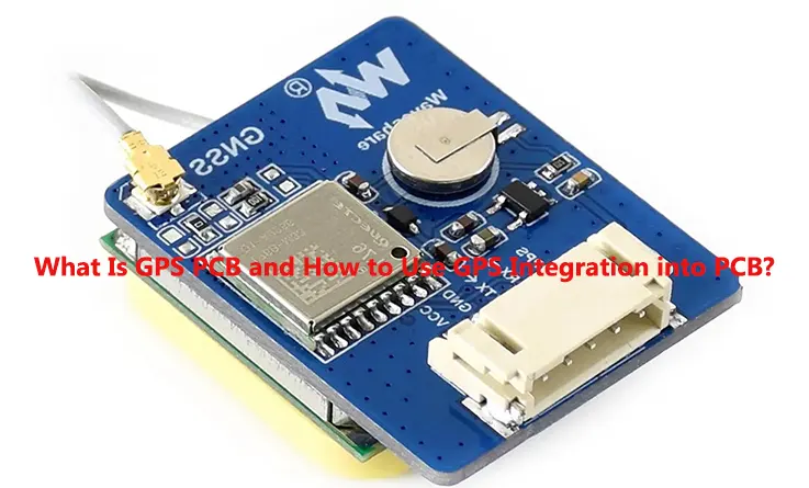
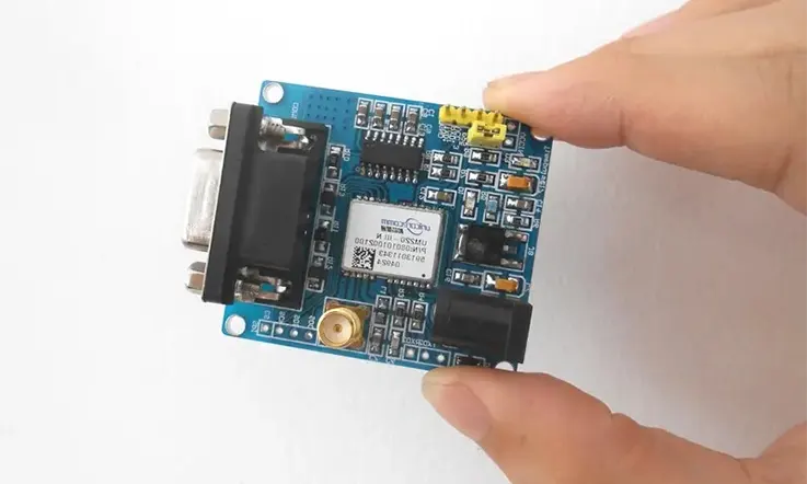
A GPS PCB is a specialized circuit board designed to integrate GPS functionality into electronic devices. It helps receive and process signals from GPS satellites, allowing for location tracking, navigation, and other location-based services.
Effective GPS PCB design involves optimizing signal integrity, minimizing power consumption, and managing environmental factors like thermal effects. This guide will explore the main aspects of GPS PCB design, including antenna integration, signal testing, and best practices for routing and layout. By understanding these factors, you can design a GPS-enabled system that meets the demands of modern applications.
What Is a GPS PCB and How Does It Work?
A GPS PCB is a specialized printed circuit board built to handle satellite signal reception, amplification, filtering, and geolocation processing. From tracking a long-haul truck making its way across the interstate to managing navigation systems in electric vehicles, this type of board keeps everything locked onto satellite data with precision. The structure, component layout, and routing strategies on this board make all the difference. Let’s pop the hood and dig into the engine room of these boards to see how they get the job done.
Understanding the Basics of GPS PCB Design
Creating a GPS PCB takes more than just wiring up a few modules. It requires an understanding of RF behavior, impedance control, and electromagnetic compatibility (EMC). During layout, we must to pay close attention to antenna placement, transmission line tuning, and multi-layer grounding.
Table 1: Design Factors That Influence GPS PCB Performance
| Parameter | Focus Area | Design Insight |
| RF Trace Routing | Minimal, direct paths | Helps prevent signal degradation |
| Ground Plane Layout | Continuous, low-impedance ground | Supports clean RF return paths |
| Shielding Techniques | Metal shields, ground pours | Reduces coupling and outside interference |
| PCB Substrate | Low-loss materials like Rogers | Supports better high-frequency signal propagation |
| GPS Module Integration | Placement near antenna, minimal vias | Reduces noise, improves Time to First Fix (TTFF) |
A slip-up in stack-up design or impedance tuning might throw off your signal, leading to poor GPS lock times or unstable operation. That’s not the kind of problem you want showing up during a product field test.
Core Components of a GPS PCB: Antenna, LNA, and Filter
For a GPS PCB to function properly, it must include specific RF components that work in tandem to pull in clean satellite data. Let’s look at three core components that drive performance:
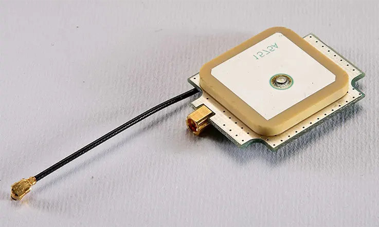
1.GPS Antenna: Responsible for receiving L-band signals from satellites, this component varies based on application. You’ll find ceramic patch antennas in vehicle trackers and chip or helix antennas in wearables. Active antennas include onboard amplification, while passive ones require external signal boost.
2.Low-Noise Amplifier (LNA): Located directly after the antenna in the RF chain, the LNA amplifies faint signals without adding excess noise. Using an external LNA can improve reception in weak-signal zones like tunnels, underground garages, or heavily shielded areas.
3.SAW Filter: Placed between the LNA and GPS module, this filter blocks unwanted RF bands (such as GSM or LTE) that may otherwise bleed into the GPS signal. The result is cleaner input to the GPS baseband processor.
●Tip: Always keep the antenna-to-LNA trace length short, straight, and well-matched to 50-ohm impedance. Any detour or mismatch could sap your signal quality.
How GPS PCBs Receive and Process Satellite Signals?
1.Satellite Signal Reception: The GPS antenna picks up RF signals from at least four satellites, broadcasting at around 1575 MHz or 1176 MHz, depending on the system (e.g., GPS, GLONASS, Galileo).
2.Amplification and Cleaning: The signal is then sent through an LNA, followed by a filter that knocks out noise from adjacent bands. These steps are what make the data usable for baseband processing.
3.Data Calculation: The GPS module performs triangulation using timing data from each satellite. Through this, it calculates latitude, longitude, altitude, and speed — all processed in real time.
●Industry Example: In a smart logistics system, GPS PCBs like these allow fleet managers to monitor driver routes, idle time, and delivery checkpoints with real-time geofencing capabilities.
●Quick Insight: Satellite signals that arrive at Earth are incredibly weak — around -130 dBm. That’s less power than background noise inside most electronics labs. It takes proper filtering and amplification to make those signals usable.
The Core Functions of GPS PCBs in Electronic Devices
In many electronic systems, the GPS PCB plays a supporting role in enabling location tracking and precise timing functionality. Its architecture is designed to facilitate reliable interaction with satellites and maintain consistency across various applications, from navigation systems to industrial control platforms. The following sections explore how GPS PCBs manage signal communication and maintain positioning accuracy in modern electronic devices.
Providing Location and Timing Data in GPS Devices
GPS PCBs support global positioning functionality by capturing signals from satellite constellations and translating them into geographic and time-based data. These signals, transmitted at specific frequencies, are received by the GPS antenna and routed through the circuit for processing.
Core Process in GPS Timing and Location Conversion-
| Stage | Function Description |
| Antenna Reception | Captures satellite signals at designated GNSS frequencies |
| LNA Amplification | Amplifies weak satellite signals with minimal noise addition |
| Filtering Stage | Removes out-of-band noise and interference |
| Satellite Signal Sync | Matches signal timestamps with satellite atomic clocks |
| Data Interpretation | Converts satellite data into real-time location and timing output |
This mechanism ensures compatibility with systems such as GPS, GLONASS, Galileo, and BeiDou. Devices using GPS PCBs can perform timing synchronization and route planning with consistent performance, depending on the design precision and environmental noise control.
How GPS PCB Enhances Device Accuracy and Reliability?
The structural and electrical integrity of a GPS PCB affects signal clarity, timing precision, and system stability. A well-designed board minimizes signal loss and electromagnetic interference.
Core factors that influence performance include:
●Impedance Control: Prevents signal reflections and maintains waveform integrity across RF transmission lines.
●PCB Stack-Up Design: Isolates power, ground, analog, and digital layers to control cross-talk and minimize coupling.
●Component Layout: Ensures short signal paths between the antenna, LNA, filter, and GPS module.
●EMI Management: Ground planes, shielding, and decoupling capacitors reduce external and internal noise sources.
For example, in automotive applications, GPS PCBs integrated into infotainment and advanced navigation modules are typically designed with RF shielding, precise trace width control, and multi-frequency support to maintain positioning accuracy under challenging conditions.
GPS PCB’s Role in Signal Transmission and Reception
To maintain usable signal quality, GPS PCBs are structured to optimize the entire transmission-reception chain, from antenna interface to digital processing. These signals, originating from satellites thousands of kilometers away, are inherently weak and must be handled with care.
Transmission and Reception Techniques-
●High-Performance Filters: Surface Acoustic Wave (SAW) or dielectric filters are applied to restrict input to desired GNSS frequency bands.
●Low-Noise Amplifiers (LNA): Selected based on gain, noise figure, and input matching for maximum signal strength.
●RF Trace Design: Uses techniques such as microstrip or grounded coplanar waveguide to manage signal integrity.
Environmental and mechanical factors, such as antenna placement, ground plane size, and enclosure materials, also influence reception quality. Devices intended for metal casings or embedded installations often require matched antennas or custom tuning to maintain consistent connectivity.
The Importance of Signal Integrity in GPS PCB Design
In GPS PCB applications, signal accuracy is not something to leave to chance. While many design teams focus on antenna placement or module selection, the electrical pathways that carry satellite signals through the circuit demand just as much care. Even minor impedance mismatches, reflection points, or unshielded segments can lead to degraded performance across navigation, tracking, and timing systems. So, let’s walk through some of the engineering considerations that influence signal integrity inside GPS PCB layouts.
Impedance Matching in GPS PCB Design
Impedance matching isn’t just a theoretical concept — it has very real consequences on GPS circuit behavior. When RF traces on the PCB don’t match the characteristic impedance (typically 50 ohms for GPS signal paths), part of the signal energy reflects back toward the source. That results in reduced signal strength at the receiver and lower signal-to-noise ratio.
Key Methods Used in Impedance Control:
| Technique | Description |
| Microstrip / Coplanar Design | Controlled-width traces routed over a ground plane to stabilize impedance |
| Dielectric Constant Selection | PCB substrate (like FR4, Rogers, or Teflon) affects trace impedance |
| Layer Stack Optimization | Signal layers and ground planes spaced to balance field propagation |
| Termination Techniques | Series or parallel resistors placed to absorb reflected signals |
Using impedance calculators, RF layout engineers can simulate trace geometries and tune the layout accordingly before manufacturing even begins. Matching connectors, cable interfaces, and module inputs must all be part of this same design review.
Minimizing Signal Loss and Noise in GPS Circuits
Satellite signals arrive at the earth’s surface with extremely low power, often below –130 dBm. That means even the smallest interference or path loss on the PCB can jeopardize the device’s ability to maintain a stable fix. GPS circuits must be engineered to support low-noise amplification, shielded routing, and power filtering to keep that noise floor down.
Strategies Commonly Applied-
●LNA Placement: The low-noise amplifier should be as close as possible to the GPS antenna, ideally within 10–15 mm.
●Via Optimization: Reducing via count along the RF signal path limits signal discontinuities.
●Guard Traces: Grounded copper traces around RF lines block crosstalk from nearby signals.
●Power Supply Decoupling: Capacitor arrays placed near active ICs help reject ripple and transient spikes.
In one commercial GPS tracking product, moving the LNA 5 mm closer to the antenna resulted in a 2 dB improvement in carrier-to-noise ratio (C/N₀), significantly helping acquisition under canopy or in dense environments.
Ensuring Accurate GPS Data Transmission
Once a GPS signal is filtered, amplified, and digitized, it must reach the host system without degradation. Data lines carrying GPS NMEA or binary output — typically via UART, SPI, or I2C — also require care in routing and signal conditioning. Though slower than RF paths, they are just as sensitive to board layout.
Design Areas to Watch-
●Line Routing Symmetry: Differential pairs (e.g., UART TX/RX) benefit from equal trace length and spacing.
●Isolation from RF Paths: Keep digital lines away from the RF front end to avoid coupling.
●Timing Considerations: For time-pulse or 1PPS output, trace length and matching must be controlled to maintain nanosecond-level timing offsets.
GPS PCBs used in high-precision applications like GNSS timing modules or autonomous navigation rely on tight timing alignment. For instance, a deviation of just 10 ns can shift a location estimate by 3 meters.
Choosing the Right Materials for Your GPS PCB
Selecting suitable materials during the early design stages of a GPS PCB can directly influence signal clarity, durability under environmental stress, and the stability of frequency-related performance. For industries like automotive electronics, aerospace GPS modules, and mobile tracking systems, this is not just a matter of preference—it shapes real-world usage outcomes. Let’s explore some of the main technical considerations that guide material selection.
Best Substrate Materials for GPS PCBs
GPS systems rely on consistent electromagnetic behavior, which is directly influenced by the base material of the PCB. Common substrate choices include:
| Material | Dielectric Constant (Dk) | Loss Tangent | Application Use Case |
| FR-4 | 4.4 – 4.7 | 0.015 | Consumer GPS devices |
| Rogers 4350B | 3.66 – 3.76 | 0.0037 | Automotive navigation |
| Teflon (PTFE) | ~2.1 | 0.0002 | High-frequency GPS applications |
●FR-4 is economical but comes with variability in dielectric properties, which may lead to slight signal deviations in precision-demanding setups.
●Rogers materials offer more predictable electrical characteristics, making them a solid choice for applications where consistent GPS timing and accuracy are needed.
●Teflon-based substrates, often used in aerospace and satellite-linked GPS modules, allow high-frequency signals to propagate with minimal loss.
These materials can be tailored based on environmental resistance (such as temperature variation), signal frequency, and cost limitations. If you’re designing for rugged environments—say fleet GPS tracking across multiple climates—your substrate choice can’t be overlooked.
The Role of Dielectric Constants in GPS Performance
The dielectric constant (Dk) of a PCB material affects how quickly electromagnetic waves can travel through it. In GPS modules, where frequencies often fall in the 1.575 GHz band (L1), maintaining a stable Dk across temperature and humidity changes helps ensure accurate signal timing.
Lower Dk values allow for faster signal propagation and reduced phase delay, while higher Dk values can compact the design at the cost of potentially increasing signal delay. We need to weigh layout compactness against timing performance.
| Frequency | Material Type | Expected Delay (ns/inch) |
| 1.575 GHz | FR-4 | 6.0 |
| 1.575 GHz | Rogers 4350B | 5.2 |
| 1.575 GHz | Teflon/PTFE | 4.0 |
In applications like GPS timing synchronization for telecom base stations, even nanosecond-level delays can stack up, so understanding Dk isn’t optional—it’s part of staying in sync with global positioning networks.
How Material Choice Affects Signal Propagation?
Material loss characteristics, such as loss tangent and surface roughness, influence how GPS signals are handled on the PCB layer. Signal attenuation can lead to degraded satellite link performance and unstable navigation readouts.
Here’s what affects signal behavior:
●Loss Tangent: Higher values indicate more signal loss as it travels through the PCB. Low-loss materials like PTFE help retain signal power over longer trace lengths.
●Surface Roughness: Rough copper interfaces scatter high-frequency waves more than smooth surfaces. For GPS frequencies, smoother copper (e.g., rolled annealed) helps maintain clarity.
If your design involves multiple GPS channels or MIMO configurations, controlling losses helps each signal path perform consistently.
How Integrating GPS Functionality into Your PCB Design?
Integrating GPS capabilities into a PCB structure demands detailed attention to signal integrity, material selection, and layout strategy. For manufacturers of communication hardware, GPS device OEMs, automotive system developers, and PCB engineers alike, aligning physical design with RF performance can reduce development challenges and support consistent positioning accuracy across multiple environments. Below, we explore how this integration process can be managed step-by-step.
GPS Antenna Integration for Efficient Signal Reception
The antenna is a critical interface in GPS PCBs, acting as the first touchpoint for satellite signals. In PCB design, patch antennas or ceramic chip antennas are commonly used. A major consideration is positioning the antenna to minimize obstructions and interference. Keeping a clear line of sight and isolating it from noisy digital components can make a measurable difference in signal acquisition time and signal-to-noise ratio (SNR).
Comparison of Common Antenna Types for GPS PCB-
| Antenna Type | Size | Gain Level | Application Suitability |
| Patch Antenna | Medium | Moderate | Automotive, Drones, Wearables |
| Chip Antenna | Small | Low | Ultra-compact GPS devices |
| Active Antenna | Medium to Large | High | Outdoor or high-sensitivity use |
Layout best practices include:
●Maintaining a ground-free zone under the antenna.
●Avoiding vias in the RF trace to reduce loss.
●Using a matching network to ensure impedance alignment.
How to Embed GPS Modules into PCBs for Seamless Operation?
GPS modules are available as shielded, surface-mounted units that include the RF frontend, processor, and often an embedded antenna. To achieve integration, we can typically embed these modules into multilayer PCBs while maintaining a clear understanding of stackup and trace impedance.
Best Practices:
●Use controlled impedance routing for RF lines.
●Ensure clear separation between analog and digital ground planes.
●Keep trace lengths between the GPS module and microcontroller short and consistent.
Application: In vehicle tracking systems, our designers often isolate GPS modules on a dedicated RF layer in a 6-layer PCB to avoid cross-interference from CAN Bus or GSM signal lines.
Minimizing Power Consumption in GPS Integration
GPS modules may consume substantial power, especially during signal acquisition. Efficient power management is necessary for battery-powered GPS applications such as IoT sensors and personal navigation devices.
Design Tips for Lower Power Usage-
●Implement a power control IC to toggle the GPS module on/off as needed.
●Use backup batteries or supercapacitors to maintain RTC time without full module power.
●Apply low-dropout (LDO) regulators with efficient thermal properties to reduce waste.
Table: Power Profiles of Common GPS Modules
| Module Name | Average Power Use (mW) | Sleep Mode Support | Fix Update Rate |
| u-blox NEO-6M | 36 | Yes | 1Hz – 5Hz |
| Quectel L76 | 25 | Yes | 1Hz |
| MediaTek MT3339 | 30 | Yes | 1Hz |
GPS power optimization is often achieved by combining efficient circuitry with firmware-controlled sleep strategies. Engineers working with wearable GPS products should assess power budget early in the design process to align with real-world usage profiles.
How to Address Common GPS PCB Design Challenges?
Designing a GPS-enabled PCB involves dealing with multiple engineering constraints. These include signal path integrity, thermal behavior, electromagnetic compatibility, and durability under variable environmental conditions. Each of these elements influences how reliably the device functions under real-world operational loads. This section outlines several methods to address practical challenges often encountered in GPS PCB development.
Avoiding GPS Signal Interference and Crosstalk
Interference and crosstalk are common issues that degrade satellite signal quality. Effective design strategies must include layout techniques and isolation methods that reduce electromagnetic disruptions in the GPS signal path.
●Separate high-frequency traces from low-speed signal lines to reduce coupling and unintended signal pickup.
●Implement a dedicated, continuous ground plane beneath RF traces to maintain return path consistency.
●Integrate band-specific filters between the GPS antenna and LNA (low-noise amplifier) to block out-of-band interference.
●Use shielding enclosures to isolate sensitive GPS circuitry from external radiation sources.
Managing Thermal Effects in GPS PCB Designs
Thermal variation can influence signal frequency, compromise solder joint integrity, and distort PCB shape. Proper thermal management helps maintain consistent performance, particularly in high-temperature or high-power applications.
●Select substrates with high thermal conductivity, such as ceramic-filled PTFE, to help distribute and dissipate heat efficiently.
●Use thermal vias beneath components with high power density to connect directly to internal copper layers.
●Separate power management ICs from RF components in the layout to minimize localized hotspots.
●Choose component packages such as QFN (Quad Flat No-lead) that offer better thermal efficiency under comparable power loads.
Enhancing Long-Term Reliability in Harsh Environments
GPS PCBs often operate in conditions such as high humidity, mechanical vibration, or temperature extremes—common in automotive, aerospace, and industrial equipment. Long-term reliability requires structural, electrical, and material-based approaches.
●Apply conformal coatings on the PCB surface to protect against moisture and chemical contaminants.
●Use solder alloys with high mechanical endurance, such as SnAgCu, to improve fatigue resistance under thermal cycling.
●Widen current-carrying traces and reinforce via structures to handle physical stress and vibration.
●Choose substrates like Rogers RO4003C that offer low water absorption and minimal dielectric drift under environmental changes.
Best Practices for GPS PCB Layout and Routing
Designing a GPS PCB involves careful consideration of routing and layout to achieve effective performance. This section will outline practical strategies for PCB design, focusing on reducing signal loss and enhancing the overall GPS system.
Optimizing Trace Routing for Low Loss and High Fidelity
Trace routing plays a significant role in ensuring minimal signal degradation and maintaining the accuracy of GPS data. Below are some practical guidelines:
●Trace Length: Keeping traces as short as possible helps reduce signal degradation. Longer traces introduce additional resistance and capacitance, weakening the GPS signal. Reducing trace length improves signal quality and reduces noise interference.
●Trace Width: Selecting an appropriate trace width based on impedance specifications ensures that the signals maintain their integrity while traveling through the PCB. This minimizes the potential for signal loss.
●Controlled Impedance: Maintaining consistent impedance across traces helps prevent signal reflections and loss. Accounting for the characteristic impedance (typically 50 ohms) when routing signal lines ensures that mismatches are avoided.
●Via Usage: Limit the use of through-hole vias, as they can add unwanted inductance and capacitance to the signal path. Blind and buried vias are more appropriate for high-frequency signals like those in GPS systems, as they maintain cleaner signal routing.
Using Ground and Power Planes Effectively in GPS PCBs
Ground and power planes are central to maintaining the reliability of GPS signals. Using them effectively can help reduce noise and improve the overall signal performance.
●Ground Planes: A continuous ground plane offers a shield against external electromagnetic interference (EMI) and ensures stable operation of GPS modules by providing a consistent reference point for the signals.
●Power Planes: A clean and noise-free power plane ensures that the GPS module receives a steady and clean power supply. Proper design of the power plane helps reduce power-related noise and improves the quality of the GPS signal.
●Decoupling Capacitors: Decoupling capacitors placed close to the power pins of the GPS module help filter out high-frequency noise, providing a more stable power supply for the GPS system.
Managing PCB Layer Stackup for GPS Signal Integrity
The layer stackup of a GPS PCB has an impact on signal propagation and integrity. Proper stackup design ensures that GPS signals are not degraded by noise or interference.
●Multi-Layer Stackup: A multi-layer stackup, typically consisting of signal, ground, and power layers, helps isolate noise and supports more efficient routing of GPS signals. This type of stackup reduces interference and provides a better environment for high-frequency signals.
●Layer Allocation: Placing signal traces on inner layers helps shield them from external noise. This results in improved signal integrity and less disruption to GPS data transmission.
●Via Placement: Avoid placing vias directly under sensitive components. Instead, use techniques such as via-in-pad or via-backplane to minimize their impact on the GPS signal and ensure a cleaner path for signal transmission.
Testing and Validation of GPS PCBs
The design and production of a GPS PCB do not end with the physical layout and assembly. The next critical phase is testing and validation. To ensure that your GPS module operates correctly, it’s necessary to perform various tests. This stage guarantees that the PCB functions efficiently under different operating conditions, providing the necessary accuracy and reliability. Let’s dive into the essential steps involved in testing and validation, offering insights into methodologies for verifying performance and avoiding common pitfalls.
Signal Testing: Ensuring GPS Data Accuracy
Signal testing helps verify the accuracy of GPS data processed by the PCB. With high-precision demands, these tests ensure that the GPS module delivers precise location information.
●Frequency Analysis: Utilize spectrum analyzers to inspect the signal at different frequencies. This allows you to check for any interference or degradation in signal quality that could impact the GPS data.
●Signal Strength: Measure the strength of the GPS signal using a signal generator to ensure that the module can receive data from satellites without disruption. Low signal strength can lead to inaccurate positioning, and testing ensures that it meets the required thresholds for accurate reception.
●Simulating GPS Satellites: One of the most effective ways to verify data accuracy is by using a GPS signal simulator to emulate satellite signals. This helps verify the functionality of the GPS system in a controlled environment before real-world testing. By simulating various satellite constellations, we can confirm the GPS module’s ability to lock onto signals from multiple satellites and provide accurate location data.
●Data Output Comparison: Compare the GPS data output to known accurate data or benchmark sources. This can help identify if the PCB is processing and outputting GPS information correctly and promptly.
Thermal and Environmental Testing for GPS PCB Reliability
GPS PCBs must function effectively in various environmental conditions, from extreme temperatures to humidity. Proper testing under these conditions guarantees reliable performance over the product’s lifecycle.
●Thermal Testing: The GPS PCB should undergo thermal cycling tests to simulate both hot and cold conditions. This will help verify that the components do not fail under temperature extremes, which could lead to signal instability. Thermal chambers can simulate temperatures ranging from -40°C to +85°C, the standard range for GPS devices.
●Humidity and Corrosion Testing: Humidity can adversely affect PCB performance, leading to component corrosion and signal degradation. Environmental chambers that control temperature and humidity help simulate long-term exposure to these elements. This ensures that the PCB maintains its signal quality and operates optimally even in harsh weather conditions.
●Vibration Testing: GPS systems in devices like drones, cars, and industrial equipment are often exposed to vibrations. Subjecting the PCB to vibration testing ensures that the device performs accurately even under mechanical stress. This test is essential for devices that will experience constant motion or shocks.
Common Pitfalls in GPS PCB Testing and How to Avoid Them?
Testing GPS PCBs involves multiple steps, but common pitfalls can lead to inaccurate results or missed issues. Understanding these challenges can save time and prevent costly mistakes.
●Overlooking Interference Sources: External electromagnetic interference (EMI) can significantly affect GPS signal quality. Failing to account for sources of EMI, such as nearby electronics, can lead to faulty signal readings during testing. Shielding the PCB with a Faraday cage or similar methods can reduce this issue during tests.
●Neglecting to Test All Operating Conditions:Testing GPS PCBs only under ideal conditions may lead to inaccurate performance assessments. Real-world use often involves fast movement, limited satellite access, and urban environments with signal reflection or blockage. Validation should include these scenarios to ensure consistent signal behavior and data accuracy after deployment.
●Not Performing Long-Term Reliability Tests: Short-term testing provides a snapshot of the PCB’s performance, but long-term testing is necessary to assess how the PCB will hold up over time. Accelerated aging tests can simulate long-term use and help identify potential failure points that might arise months or years after deployment.
●Ignoring Signal Integrity Issues During Production: Poor PCB design practices or poor soldering quality can affect the integrity of GPS signals. Small issues, such as improper trace width or via placement, can lead to signal loss that may not be noticeable in initial tests but will manifest in real-world use. Ensuring signal integrity during production can help avoid this pitfall.
The Future of GPS PCBs
The evolution of GPS PCBs is closely linked with the expansion of embedded systems and multi-protocol connectivity. As design parameters become more demanding—requiring compact size, low power, high-frequency operation, and environmental resilience—the future direction of GPS integration calls for more predictive engineering and multi-domain optimization. This section outlines how AI, miniaturization, 5G, and IoT are contributing to changes in design methodologies and layout considerations.
How AI and Machine Learning Are Shaping GPS PCB Design?
Artificial intelligence and machine learning are being adopted in advanced EDA workflows to assist in GPS PCB design. These tools can analyze complex signal pathways, automatically detect impedance mismatches, and predict electromagnetic interference risks before fabrication. We can gain the benefit of predictive layout optimization and quicker iterations through data-driven modeling.
Comparison Table: Conventional vs. AI-Assisted GPS PCB Design-
| Feature | Traditional Workflow | AI/ML-Assisted Workflow |
| Trace routing optimization | Manual routing based on experience | Algorithm-based dynamic optimization |
| EMI prediction | Post-layout simulations | Pre-layout prediction via model training |
| Stack-up configuration | Static, manually defined | Adaptive to signal integrity predictions |
| Iteration count | 4–6 revisions per project | Often reduced to 2–3 |
Tip: Platforms such as Altium Designer and Cadence Allegro are already incorporating these AI modules for predictive layout assistance.
Upcoming Trends in Miniaturization and Multi-Function GPS PCBs
The trend toward smaller, multifunctional devices has introduced more integrated GPS PCB modules that combine multiple RF systems such as Bluetooth, Wi-Fi, cellular, and sensors in a single design. This calls for tighter routing strategies, enhanced power efficiency, and stronger shielding against cross-domain interference.
Miniaturized GPS Module Specifications-
| Module Model | Size (mm) | Protocols Supported | Package Type | Power Consumption (Active) |
| u-blox NEO-M9N | 12.2 × 16.0 | GPS / GLONASS / Galileo / BeiDou | LCC | 29 mA |
| Quectel L76K | 10.1 × 9.7 | GPS / QZSS | Embedded Antenna | 21 mA |
| Sony CXD5610GF | 6.0 × 6.0 | GPS + Sensor Fusion | SiP | 15 mA |
Recommendation: For applications requiring compact enclosures, consider LCC or SiP modules with built-in antennas to reduce component overhead.
How 5G and IoT Are Driving the Future of GPS PCB Integration?
The adoption of 5G and the proliferation of IoT devices require GPS modules to interact efficiently with multi-band radios, advanced power regulators, and shared timing resources. This integration often includes shared TCXOs, cross-domain frequency planning, and coordinated signal routing within the same stack-up.
5G and GPS Co-Integration Technical Overview-
| Parameter | Standalone GPS Module | Co-integrated GPS + 5G/IoT Module |
| Antenna isolation | Single-band requirements | Multi-band with enhanced filtering |
| Clock source management | Dedicated clock | Shared TCXO or VCXO for synchronization |
| Positioning precision | 2–5 meters | <1 meter with assisted GPS |
| Power regulation | Isolated LDO per module | Shared PMICs across subsystems |
Design Insight: For precision navigation or synchronized network applications, select chipsets that support LTE OTDOA or 5G NR-PRS for auxiliary location services.
GPS PCB Frequently Asked Questions (FAQ)
1.What is the typical operating frequency range for GPS PCBs?
Most GPS PCBs operate at L1 (1575.42 MHz), but multi-band systems may also use L2 and L5.
2.Can GPS PCBs be used indoors?
Standard GPS PCBs struggle with indoor signal acquisition. Assisted GPS or GNSS repeaters are often required.
3.What’s the minimum PCB layer count recommended for GPS applications?
At least 4 layers are recommended to support controlled impedance, power integrity, and grounding.
4.Do GPS PCBs require shielding?
Yes, especially in mixed-signal environments. Shield cans or EMI absorbing materials are often used.
5.What software is commonly used to simulate GPS PCB layouts?
Tools like HFSS, CST Studio, and ADS are used for high-frequency and antenna simulation.
6.How accurate is a GPS PCB without an external antenna?
Onboard antennas can deliver 3–10 meters accuracy in open areas, but performance drops significantly in dense environments.
Related Posts:
1. Exceptional Manufacturer of Antenna PCBs
2. JarnisTech – High Quality Bluetooth PCB Manufacturer
3. FAQ Guide About Wireless PCB
4. Why Carrier PCB in Telecommunication Is So Useful?
6.The Evolution of 5G PCB Technology: Transforming the Telecommunication Industry