Modern electronic systems require printed circuit boards (PCBs) engineered to perform under conditions that surpass conventional limitations. As device functionality, speed, and power density increase, the demand for circuit boards tailored to specific, high-performance applications becomes a necessity. This guide provides a technical exploration of specialized PCBs, detailing their architectures, the advanced materials used, and the complex fabrication and assembly processes involved in their creation, all while adhering to stringent industry quality standards.
Specialized PCBs: From Precision Fabrication to Full Assembly
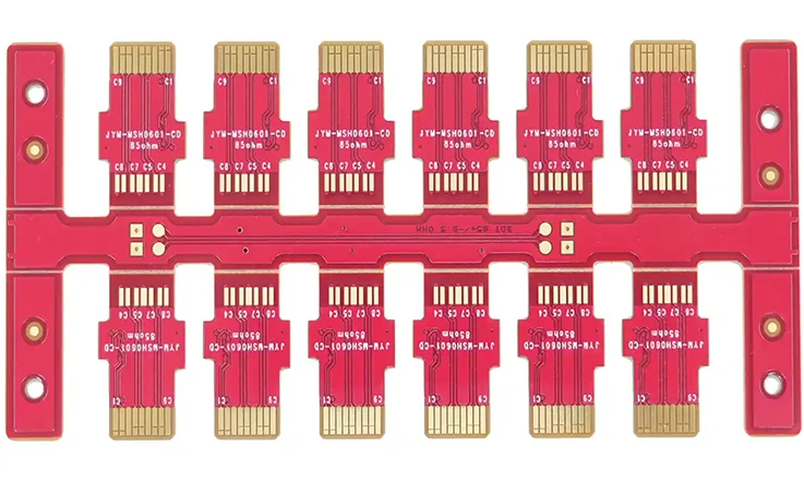
A specialized printed circuit board is engineered to perform in applications where standard boards are insufficient. Its construction involves non-standard materials, intricate layouts, and specific electrical properties to achieve superior performance and durability in demanding environments. This fabrication approach moves beyond generic templates to satisfy precise operational requirements.
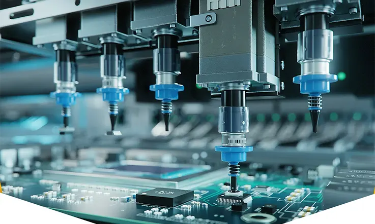
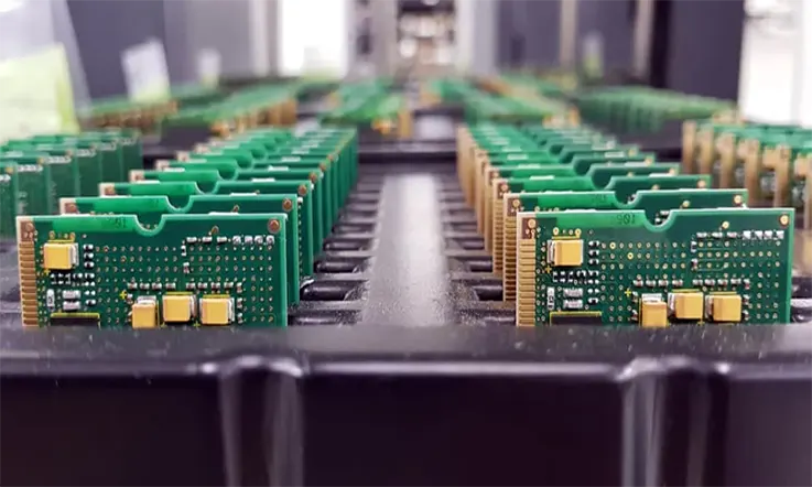
Following the custom fabrication of the board, the assembly process populates it with electronic components. This stage continues the dedication to precision, transforming a bare board into a fully operational unit ready for its intended function. The assembly service encompasses:
Component Sourcing:
Procurement of all specified electronic components, which includes managing complex supply chains for specialized or long-lead-time parts.
SMT & Thru-Hole Assembly:
Application of automated techniques for exact component placement on any board topology, including dense, double-sided, and mixed-technology assemblies.
Quality Verification:
Post-assembly inspection and functional testing to confirm that every connection and component placement adheres to stringent project specifications.
Turnkey Assembly Service:
An end-to-end process that delivers a fully assembled and tested product, prepared for final system integration.
An Overview of Specialized PCB Architectures
Specialized printed circuit boards are engineered for challenges that standard boards cannot address. Each design provides a distinct solution for specific mechanical, thermal, or spatial constraints, forming the foundation for high-performance electronic devices.
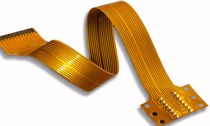
Flexible PCBs (Flex Circuits)
Constructed on pliable polymer substrates, flexible circuits can bend and fold to integrate into three-dimensional product enclosures. They offer a direct replacement for rigid boards connected with wires and connectors, especially in applications where space and weight are limited.
●Three-Dimensional Integration: Flex circuits conform to the internal contours of a product, saving significant space and weight compared to rigid board and cable harness combinations.
●Dynamic Applications: Their resilience to repeated movement makes them suitable for hinged electronics, robotics, and other applications requiring interconnection between moving parts.
●Verified Reliability: Performance is qualified against demanding standards like IPC-6013, ensuring durability for use in wearables, medical implants, and aerospace systems.
| Parameter | Typical Value/Range | Industry Benchmark |
| Minimum Bend Radius | 5–10 × board thickness | IPC-2223 compliance |
| Weight Reduction vs. Rigid PCB | 30–60% | Verified in teardown |
| Flex Cycles (Dynamic) | > 1 million | IPC-6013 Class 3 |
| Operating Temperature Range | -40°C to +125°C | Aerospace grade |
| Material Type | Polyimide, PET | UL 94V-0 rated |
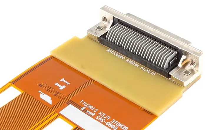
Rigid-Flex PCBs
These boards are a hybrid, combining rigid PCB sections and flexible circuits into a single, unified component. The design provides the mounting stability of a rigid board for dense component populations while offering the routing freedom of a flex circuit to interconnect these sections, which removes potential points of failure from separate cables and connectors.
Application Example: 8-Layer Rigid-Flex PCB for an Aerial Drone Gimbal
●Challenge: A three-axis camera gimbal experienced signal degradation and mechanical wear from traditional cable connections subjected to constant rotation and stress.
●Solution: An 8-layer rigid-flex board was engineered. Rigid sections provided stable platforms for the image sensor and processors, while an integrated flex tail replaced the wiring harness, moving freely with the gimbal.
●Result: The unified design resolved all connection reliability issues. It also reduced the gimbal’s weight by 25%, contributing to longer flight times, and streamlined final assembly by removing manual connection points.
| Parameter | Typical Value/Range | Industry Benchmark |
| Total Layer Count | 4–20 layers | ≥ 8 for complex apps |
| Flex Section Thickness | 0.1–0.2 mm | IPC-2223 standard |
| Bend Cycles (Dynamic) | > 500,000 | IPC-6013 Class 3 |
| Weight Reduction | 20–30% | Verified in teardown |
| Integration Efficiency | 1 unified PCB vs. ≥ 3 separate parts | Reduced interconnect failures |
High-Density Interconnect (HDI) PCBs
High-Density Interconnect (HDI) manufacturing enables a higher concentration of components and routing per unit area. This is achieved with features like laser-drilled microvias, finer traces and spaces, and advanced lamination processes, facilitating substantial device miniaturization without sacrificing functionality.
Application Example: HDI Mainboard for a Portable Medical Monitor
●Challenge: A medical device required an extremely small, wearable glucose monitor with powerful processing and extended battery life.
●Solution: A 10-layer HDI board with a (1+8+1) sequential build-up (SBU) structure was used. Stacked microvias and via-in-pad technology allowed a 0.4mm pitch BGA processor and all support circuits to be placed on a board the size of a postage stamp.
●Result: The product’s footprint was reduced by 60%. Shorter signal paths lowered power consumption, extending battery life by 40%. The HDI structure also provided a stable platform for the assembly of the fine-pitch BGA.
| Parameter | Typical Value/Range | Industry Benchmark |
| Minimum Trace/Space | 50/50 μm (2/2 mil) | Advanced HDI spec |
| Microvia Diameter | 75–100 μm | Laser-drilled |
| Layer Count | 6–16 layers | ≥ 10 for complex apps |
| BGA Pitch Capability | 0.3–0.4 mm | Via-in-pad capable |
| Size Reduction | 50–70% vs. standard | Verified in teardown |
Metal Core PCBs (MCPCBs)
An MCPCB is built on a metal base, typically aluminum or copper, for superior thermal dissipation. An electrically isolating, thermally conductive dielectric separates the circuit from the metal core, drawing heat away from power-intensive components more effectively than standard FR-4 substrates.
Application Example: Aluminum Core PCB for an Industrial LED High-Bay Light
●Challenge: A 200W LED high-bay light suffered from rapid lumen decay and a short operational life due to heat accumulation on its standard FR-4 board.
●Solution: The light engine was redesigned using a high-performance aluminum core PCB. The aluminum base efficiently transferred heat from the LED array to the fixture’s external heatsink.
●Result: The LED chips’ junction temperature dropped by a measured 35°C. This change stabilized the light output and more than doubled the luminaire’s effective lifespan.
| Parameter | Typical Value/Range | Industry Benchmark |
| Core Material | Aluminum or Copper | ≥ 1.5 mm thick |
| Thermal Conductivity | 1.5–3.0 W/m·K | ≥ 2.0 W/m·K |
| Max Operating Power | 50–300 W | LED lighting spec |
| Junction Temperature Drop | 25–40°C improvement | Verified in lab |
| Lifespan Improvement | 2×–3× | Field-tested |
Thick Copper PCBs
This category includes PCBs with copper layers exceeding the standard 1-2 oz (35-70µm) thickness. Designed for high-current applications, these boards use heavy copper traces to manage large electrical loads and aid in thermal distribution across the board.
●High-Current Capacity: With copper weights from 3 oz to over 10 oz, these boards can handle hundreds of amperes for power distribution systems, planar transformers, and automotive power electronics.
●Specialized Fabrication: Producing these boards demands advanced etching and plating processes to create fine features in thick metal and to ensure robust, even plating of through-holes.
| Parameter | Typical Value/Range | Industry Benchmark |
| Copper Thickness | 105–350 μm (3–10 oz) | Heavy copper spec |
| Current Capacity | 50–300+ A | UL 796 compliant |
| Min. Trace Width | 0.3–0.5 mm | With thick copper |
| Plated Through-Hole Wall | ≥ 25 μm | IPC Class 3 |
| Thermal Conductivity | ~ 385 W/m·K (Cu) | Material property |
Advanced PCB Materials: A Foundation for Performance
The performance of a specialized printed circuit board is determined by its material foundation. While the glass-epoxy laminate FR-4 is a versatile standard, advanced electronic designs require substrates with specific electrical, thermal, and mechanical properties that FR-4 cannot provide. The choice of substrate is a primary engineering decision that dictates the final capabilities of the device.
Polyimides (PI)
Polyimide is a high-performance polymer serving as the base material for most flexible and rigid-flex PCBs. It is selected for its combination of thermal stability, chemical resistance, and mechanical durability, making it a frequent choice for high-reliability applications.
●Operation in Demanding Environments: Its inherent properties make it suitable for aerospace, military, and medical devices that must operate without failure under strenuous conditions.
●Assembly Resilience: It dependably withstands the high temperatures of modern lead-free soldering, protecting board and component integrity during the assembly phase.
Fluoropolymers (e.g., PTFE)
Polytetrafluoroethylene (PTFE) and similar fluoropolymers are specified for high-frequency RF and microwave circuits. For these designs, preserving the purity of signals is the main objective.
●Signal Integrity: A very low and stable dielectric constant (Dk) and dissipation factor (Df) are the defining traits of these materials, which minimizes energy loss and preserves signal clarity at high frequencies.
●Specialized Fabrication: Fabricating and assembling circuits on PTFE demands unique techniques. The material’s distinct characteristics, such as softness and thermal expansion, require specialized handling throughout the production process.
Advanced Hydrocarbon & Ceramic-Filled Laminates
This category of materials offers a tailored performance profile, positioned between conventional FR-4 and high-performance fluoropolymers. They provide an engineered solution for designs that need better electrical performance than FR-4 without the extreme low-loss properties or associated cost of PTFE.
●Balanced Electrical Performance: They exhibit improved electrical characteristics over FR-4, making them a fit for applications like automotive radar and high-speed digital networks where signal attenuation is a concern.
●Manufacturability: These laminates are formulated to be processed with more conventional methods than PTFE, which can benefit fabrication yields and predictability during both board manufacturing and final assembly.
Ceramic Substrates
For applications operating in extreme thermal or environmental conditions, ceramic substrates like Alumina (Al2O3) and Aluminum Nitride (AlN) provide exceptional stability and thermal management beyond the capabilities of any polymer-based material.
●Superior Heat Dissipation: Their high thermal conductivity offers an efficient pathway for heat to escape from high-power components like power semiconductors and laser diodes.
●Stable Component Foundation: The rigidity and low coefficient of thermal expansion of ceramics provide a solid foundation for mounting sensitive components that must function reliably in harsh, high-temperature environments.
The PCB Stack-up: An Engineered Foundation for Performance
The layer stack-up is the blueprint for a multi-layer PCB, defining the precise arrangement and materials of its internal structure. This engineering document governs the board’s electrical characteristics, from impedance control to the containment of electromagnetic interference (EMI). A well-executed stack-up is a primary factor in achieving a high-performance outcome.
Stack-up Construction: Cores and Prepregs
A multi-layer board is constructed by combining two primary dielectric components under heat and pressure.
●Cores: A core is a rigid piece of laminate, cured in a factory and pre-bonded with copper foil on one or both sides.
●Prepregs: Prepreg is a fibrous material, such as fiberglass, that is saturated with an uncured resin. During lamination, the resin flows to bond the cores and copper layers together, forming a monolithic structure.
●Material Specification: The specific material type and thickness of each core and prepreg are selected to achieve the target overall board thickness and desired electrical properties.
Strategic Layer Arrangement for EMI Containment
The placement of copper layers is planned to manage electromagnetic fields and prevent interference.
●Shielding High-Speed Signals: A common strategy involves routing high-speed signal layers on the inside of the board, positioned between solid ground or power planes. This creates a stripline configuration that effectively shields the signals.
●Symmetrical Construction: A balanced, symmetrical arrangement of layers is specified to prevent the board from warping during the high-temperature lamination and assembly processes, ensuring mechanical stability.
Trace Geometry and Impedance Control
The stack-up defines the physical environment that dictates the behavior of signal traces.
●Microstrip and Stripline: A trace on an outer layer with a single reference plane below it is a microstrip. A trace on an inner layer between two reference planes is a stripline.
●Impedance Calculation: The dielectric material, its thickness, and the distance between layers—all defined in the stack-up—are the determining factors for calculating the exact trace width needed to achieve a specific characteristic impedance (e.g., 50 ohms). This demands precision in both design and fabrication.
Signal Integrity in High-Speed PCB Design
In high-speed digital systems, a printed circuit board functions as an active transmission channel where physical effects can corrupt data. Signal integrity (SI) refers to the measures taken to preserve the quality of electrical signals as they travel from a transmitter to a receiver, ensuring that waveforms arrive with predictable shape and timing.
Managing Reflections and Impedance Discontinuities
A primary objective in high-speed design is to maintain a uniform characteristic impedance throughout a signal’s path.
●The Challenge: When a signal encounters a change in impedance—at a connector, via, or improperly sized trace—a portion of its energy reflects back toward the source, distorting the waveform and degrading data quality.
●The Solution: This is managed through meticulous stack-up engineering and controlled fabrication processes that produce traces with a specific, uniform impedance. Disciplined routing practices are also employed to minimize other sources of discontinuity.
Controlling Signal Loss and Attenuation
As signals travel across a PCB, their amplitude naturally decreases. This attenuation must be managed to ensure the signal can be correctly interpreted at the receiver.
●The Causes: Signal loss stems from two main mechanisms: dielectric loss, where energy is absorbed by the PCB substrate, and skin effect loss, which is resistive loss as current crowds onto a conductor’s surface at high frequencies.
●The Solution: Combating attenuation requires the selection of appropriate low-loss laminate materials and the optimization of trace geometries during the design and fabrication stages to ensure the signal arrives with sufficient amplitude.
Mitigating Crosstalk and Noise Coupling
Crosstalk is the unwanted electromagnetic coupling that occurs between adjacent signal traces on a PCB.
●The Challenge: A fast-switching signal on one trace can induce a noise pulse on a neighboring trace. This induced noise can be misinterpreted as a valid signal, causing false logic states and system errors.
●The Solution: Crosstalk is minimized by ensuring adequate spacing between parallel traces and using solid reference planes. These planes help contain the electromagnetic fields and provide a clean, low-inductance return path for the signal current.
Power Integrity (PI) for Stable System Operation
Power integrity (PI) is the practice of providing all active components on a board with a stable, low-noise power supply. As modern integrated circuits demand large, transient bursts of current, the ability of the board’s Power Distribution Network (PDN) to meet these demands governs the stability and performance of the entire system.
The Power Distribution Network (PDN)
The PDN consists of all power and ground planes, traces, and vias that deliver current from the source to the active components.
●Objective: The PDN must be designed to have the lowest possible impedance across a wide range of frequencies.
●Function: A low-impedance PDN can deliver large, instantaneous currents to an IC without a significant voltage drop, which is necessary for reliable operation.
●Fabrication: This is achieved in fabrication by creating solid, unbroken power and ground planes and ensuring a low-inductance path from the voltage source to the load.
The Function of Decoupling Capacitors
Decoupling capacitors serve as local, high-speed energy reservoirs for integrated circuits.
●Transient Current Supply: They supply the immediate, high-frequency current bursts that a distant power supply is too slow to provide.
●Assembly and Placement: Their effectiveness depends on precise placement during assembly—as close as possible to the component’s power pins—to minimize interconnect inductance.
●Decoupling Strategy: A successful design uses a spectrum of capacitor values: larger capacitors for low-frequency current demands and smaller, low-inductance ceramic capacitors for high-frequency needs.
Addressing Common PI Failures
Two common power integrity issues are IR drop and ground bounce.
●IR Drop: This is a steady-state voltage loss that occurs as current flows through the natural resistance of the power planes and traces.
●Ground Bounce: This is a transient noise spike on the ground rail, often caused when many outputs on an IC switch low at the same time.
●Mitigation: Both issues are addressed through robust PDN design and fabrication, which includes using wide power traces, solid planes, and a sufficient number of vias to minimize both resistance and inductance in the power delivery path.
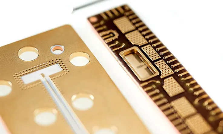
A Guide to Advanced PCB Surface Finishes
The surface finish is the metallic coating applied over exposed copper pads, forming the interface between the bare board and its components. This layer protects the copper from oxidation and provides a solderable surface for reliable component attachment during assembly. The choice of finish affects assembly yield, long-term reliability, and cost, and it determines suitability for specific processes like wire bonding or press-fit connections.
While a standard finish like Hot Air Solder Leveling (HASL) may be adequate for simple electronics, specialized PCBs with fine-pitch components or high-frequency signals demand advanced options. These finishes offer superior planarity (flatness) and durability, contributing directly to the success of complex assemblies.
ENEPIG (Electroless Nickel Electroless Palladium Immersion Gold)
Often called a “universal finish,” ENEPIG is a multi-layer coating consisting of electroless nickel, a thin barrier of electroless palladium, and a final flash of immersion gold. The palladium layer prevents nickel from migrating into the gold, which mitigates the risk of brittle solder joints.
●Provides an exceptionally flat surface, suitable for fine-pitch BGA and other high-density components.
●Offers a wire-bondable surface for both gold and aluminum wire.
●The multi-layer structure ensures outstanding long-term reliability and an extended shelf life.
●It is a preferred, though more costly, option for the most demanding applications.
Hard Gold (Electrolytic Nickel Hard Gold)
This finish is engineered for extreme durability and wear resistance. It consists of a thick layer of gold (typically 30-50 microinches), hardened with cobalt or nickel, plated over a base of electrolytic nickel.
●Its primary application is for high-wear areas requiring repeated mechanical contact, such as edge-connector fingers, keypads, and test points.
●While not intended for soldering large areas due to the risk of solder embrittlement, it is the standard for applications where the physical toughness of the contact surface is the main objective.
Immersion Silver (IAg)
Immersion Silver is a lead-free finish applied directly over the copper via a chemical displacement reaction, offering excellent planarity at a moderate cost.
●The very flat surface makes it a good choice for fine-pitch component assembly.
●Its low signal loss is beneficial for certain high-frequency applications.
●Its susceptibility to tarnishing from environmental exposure necessitates specialized handling and packaging protocols to preserve solderability.
Immersion Tin (ISn)
This is another planar, lead-free finish created by a chemical reaction with the base copper, often used for press-fit connector applications.
●Provides an exceptionally flat and reliable surface for soldering.
●Modern formulations have minimized, but not eliminated, the risk of “tin whisker” growth—tiny, conductive filaments that can cause short circuits in long-life applications.
●The finish has a more limited shelf life compared to gold-based alternatives.
Advanced Assembly Processes for Specialized PCBs
Specialized boards require advanced assembly processes to ensure reliability and performance. The assembly of complex, high-density boards is a precision discipline where quality is verified against rigorous standards, such as IPC-A-610 Class 3 for high-reliability electronics.
Package-on-Package (PoP) Assembly
This advanced Surface Mount Technology (SMT) technique involves stacking one integrated circuit package directly on top of another, such as placing a memory package on a processor.
●Benefit: This three-dimensional packaging method saves considerable board space, enabling greater functionality in smaller product footprints.
●Process: A successful PoP build is a multi-stage process that demands meticulous control over solder paste application, placement accuracy, and multiple, carefully engineered reflow profiles.
BGA Underfill Application
For large Ball Grid Array (BGA) components subjected to mechanical stress or thermal cycling, a specialized epoxy underfill is applied beneath the package after the primary soldering process.
●Benefit: This epoxy distributes stress away from the delicate solder connections and across the entire component body, substantially increasing the assembly’s durability against shock and vibration.
●Process: The underfill material is dispensed and then cured using controlled thermal profiles to ensure a complete, void-free application that provides maximum mechanical reinforcement.
Conformal Coating Services
For assemblies that will operate in demanding or corrosive environments, a thin, protective polymer film is applied to conform to the shape of the populated board.
●Benefit: The coating shields the circuitry and solder joints from performance-degrading factors like moisture, dust, and chemicals, preventing corrosion and extending the product’s operational life.
●Process: Application can be performed using various methods, including precision automated spraying or dipping, selected based on board complexity and coverage requirements to ensure a uniform, protective barrier.
Evaluating a High-Capability Manufacturing Partner
After defining the design and materials for a specialized PCB, the final step is selecting a manufacturing partner capable of transforming the blueprint into a reliable product. This evaluation extends beyond a simple price comparison to a holistic assessment of a partner’s quality systems, engineering support, and proven technical capabilities. The following benchmarks can guide the selection of a partner equipped to handle complex projects.
A Foundational Commitment to Quality
A premier manufacturing partner embeds quality into every stage of the process, rather than treating it as a final inspection point. Look for evidence of:
●Strict and verifiable adherence to high-reliability standards such as IPC-6012 for fabrication and IPC-A-610 Class 3 for assembly.
●A robust quality management system that includes full material traceability from sourcing to shipment.
●Comprehensive in-process inspections at multiple manufacturing stages.
●Advanced final verification methods, including microsection analysis and Time Domain Reflectometry (TDR) impedance testing.
| Quality Metric | Industry Standard/Method | Target Level |
| Fabrication Standard | IPC-6012 | Class 3 |
| Assembly Standard | IPC-A-610 | Class 3 |
| Material Traceability | ERP/QMS System | 100% batch traceability |
| In-Process Inspection Frequency | AOI/X-ray at multiple stages | ≥ 3 checkpoints |
| Final Verification | Microsection & TDR | ±5% impedance tolerance |
Transparent Pricing and Total Value
The true expense of a PCB is its total cost of ownership, not its upfront price. A valuable partner focuses on delivering reliability that prevents costly field failures. Indicators of this approach include:
●Clear, transparent pricing structures with no hidden costs.
●A focus on achieving high first-pass yields to avoid schedule delays and rework.
●The offering of a complimentary, in-depth Design for Manufacturability/Assembly (DFM/DFA) analysis before production begins to identify and resolve potential issues early.
Predictable Scheduling and Proactive Management
Time-to-market is a deciding factor in product development. A capable partner manages this through diligent oversight and clear communication. Hallmarks of this capability are:
●A single-point-of-contact project management style that ensures clear accountability.
●Proactive and consistent communication with regular status updates.
●Strong relationships with material suppliers to anticipate and mitigate material sourcing delays.
Responsive and Accessible Engineering Support
Complex projects often present technical challenges. A superior partner provides direct access to experienced engineering talent throughout the project lifecycle. This should include:
●A collaborative approach to solving difficult design issues efficiently.
●Actionable feedback on design choices from the initial quote through to final delivery.
●Technical depth that reflects a genuine understanding of advanced PCB technologies.
Verifiable Advanced Capabilities
A partner’s stated capabilities must be verifiable and aligned with the demands of specialized PCBs. This includes demonstrated proficiency with:
●High layer counts (20+ layers).
●Any-layer High-Density Interconnect (HDI) technology.
●Processing a diverse range of RF, microwave, and high-speed digital materials.
●Heavy and extreme copper fabrication.
●Maintaining tight tolerances on impedance (e.g., ±5%) and fine-line geometries.
| Capability | Technical Specification | Benchmark |
| Layer Count | Maximum layers supported | ≥ 20 |
| HDI Capability | Any-layer / Stacked Microvias | Yes |
| RF/Microwave Materials | Rogers, Taconic, Isola, etc. | Full processing support |
| Copper Thickness | Heavy/Extreme Copper | Up to 20 oz |
| Impedance Control | Tolerance level | ±5% |
| Fine-Line Width/Spacing | Minimum manufacturable | 2.5 mil / 2.5 mil |
Frequently Asked Questions (FAQ)
Q1: What is a “keep-out” zone in a rigid-flex design?
A: It’s a specified area on the flexible part of the board, especially near the transition to the rigid section, where no components, vias, or sharp trace turns should be placed. This prevents mechanical stress and potential cracking during bending.
Q2: For impedance control, is it better to adjust trace width or dielectric height?
A: It is almost always better and more practical to adjust the trace width. The dielectric height is fixed by the chosen prepreg in the board’s stack-up, while trace width can be precisely controlled during the etching process for fine-tuning.
Q3: What does “aspect ratio” mean in PCB drilling?
A: It’s the ratio of the hole’s depth to its diameter. A high aspect ratio (e.g., >10:1) is challenging because it is difficult to achieve even copper plating inside a deep, narrow hole, potentially leading to unreliable via connections.
Q4: What is “delamination” and what causes it?
A: It is the separation of layers within a PCB. It is a serious defect often caused by trapped moisture in the laminate expanding during high-temperature assembly, or by an improper lamination cycle (incorrect heat or pressure).
Related Posts:
1.How to Build a Heater PCB Circuit Boards?
2.What is a Round Printed Circuit Board (PCB)?