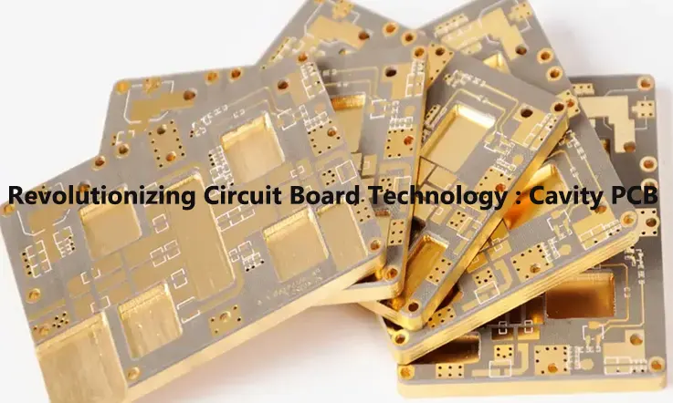
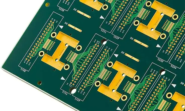
PCB incorporate various technologies to enhance their performance, and one such strategy is the implementation of cavity PCB. Cavity PCB feature indentations or hollowed areas on the board, which serve to ensure precise dimensions and accuracy.
Employing cavities in PCB provides multiple benefits, particularly in relation to component positioning and assembly. By incorporating these indentations, the component incorporating these indentation becomes more streamlined and efficient. Moreover, the assembly procedure is uncomplicatedly streamlined, promoting increased productivity efficiency.
Should you possess any queries pertaining to cavity PCB, rest assured you have arrived at an apt platform. In this post, we will address several fundamental questions, providing you with a comprehensive understanding of PCB cavities. The perusal of this article, you can expect your queries concerning cavity PCB to be thoroughly answered.
What is Cavity PCB?
Printed circuit board, or PCB, function as the core substrate for electrical constituents and facilitate the creation of specific electrical functions across a vast spectrum of electronic apparatuses.
In most cases, PCB consist of multiple layers that need to be interconnected to ensure their functionality. One methodology to actualize this involves the assimilation of cavities on the PCB – these constitute perforations or apertures executed to facilitate the connection of these strata.
To create cavities, holes are typically drilled through the outer copper layer of the PCB and extend into the inner layers, stopping short of penetrating all layers of the board.
Cavities primarily serve to reduce the overall height of the components they surround. Their purpose is to enhance the clearance between components on the board.
Considering the current focus on downsizing components and devices, cavities hold significant importance in PCB. They play a crucial role in accommodating the shrinking dimensions and improving the overall performance of electronic systems.
Types of Cavity PCB
Various electronic applications often utilize a range of cavity PCB. Among the frequently used types are:
Through-Hole Cavity PCB: Varieties of cavity PCB falling into this category bear cavities drilled with through-hole via that establish a connection between the top and bottom layers of the board. The via are pierced through the entire board, then plated to yield electrical conductivity.
Blind Via Cavity PCB: Cavity PCB of this type feature cavities equipped with blind via that bind the top and interior layers of the board. The via are drilled only partially through the board, and then plated to provide electrical conductivity.
Buried Via Cavity PCB: These cavity PCB exhibit cavities boasting buried via connecting the inner layers of the board. Such via are drilled and plated prior to the layer lamination process, rendering them less discernible on the board’s surface.
Stacked Via Cavity PCB: In this type of cavity PCB, cavities possess stacked via that link numerous inner layers of the board. These via are drilled and plated in a sequential manner, which enables reducing the overall dimensions of the board while boosting the layer count.
Metal Core Cavity PCB: This types of cavity PCB incorporate a metallic core stratum intermediate to the top and bottom layers of the board. This metal core amplifies thermal conductivity, thus making these PCB types an optimal fit for high-power demanding applications.
These are just a few examples of the types of cavity PCB that are available. The types of cavity PCB utilized is contingent upon the necessities of the particular use-case. Including factors such as: size and shape of the cavity, layer count necessary and the desired electrical and thermal properties.
Construction of the Cavity PCB
Cavity PCBs offer additional functionality compared to standard PCBs due to their structural recesses. One notable advantage is the ability to incorporate heat sinks called “coins,” which are inserted into the cavities. These coins facilitate the positioning of electronic components below the surface, resulting in a slimmer overall profile for the assembled printed circuit board.
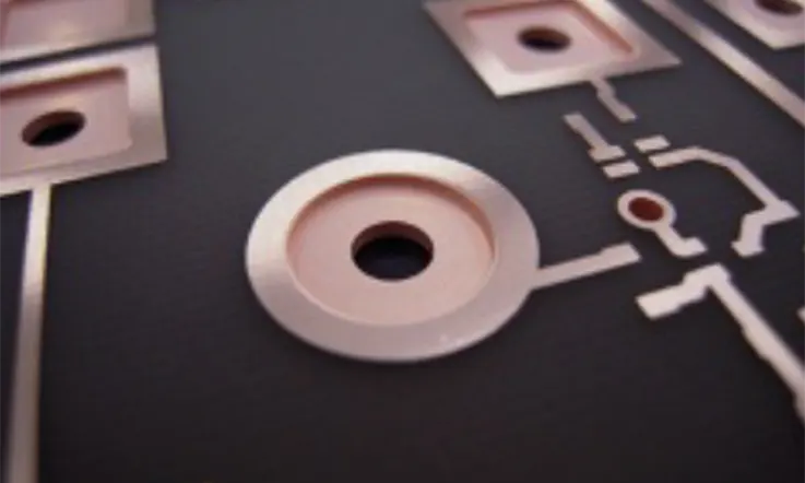
Moreover, the inner surfaces of the cavities can be utilized for electrical contacts, typically for grounding purposes. While there are various methods to create a cavity in a printed circuit board, the most common approach involves mechanical removal of material from the PCB structure to form window-shaped recesses in multilayer PCBs.
During the assembly of prepreg and laminate materials, these layers form the walls of the cavities. In situations where the cavity functions as a microwave/RF resonant cavity, the frequency is determined by the cavity’s size, and it is crucial for the PCB manufacturer to control the X, Y, and Z dimensions of the cavity. The cavity designs can be implemented in multiple locations on a single PCB, with different depths, and can even be edge plated if required.
Design Considerations for Cavity PCB
When creating a cavity PCB it’s crucial to consider important factors to guarantee the board operates as planned. Some key things to think about when designing a cavity PCB are:
Cavity size and shape: The size and shape of the cavity will depend on the specific application requirements. The cavity ought to be of sufficient dimension to house the components and requisite structures, yet simultaneously adhering to the confinements of the board’s size and thickness.
Cavity placement: The position of the cavity on the board also hinges on the application directives. The cavity must be strategically situated to facilitate optimum thermal dissipation and electrical connectivity.
Component placement: The strategic arrangement of components within the cavity warrants meticulous consideration to ascertain their appropriate mounting and secure fixture. The components should be positioned such that they do not interfere with each other or with the surrounding structures.
Signal integrity: The design must integrate potential implications of the cavity on the board’s electrical attributes. Trace placement and routing must be performed with caution to avert any interference or depreciation of signal strength.
Thermal management: Cavity PCB may have increased thermal management requirements due to the cavity’s presence. The board’s thermal characteristics must be analyzed meticulously ensuring efficient heat diffusion, thereby averting possible component damage.
Board thickness: The thickness of the board inherently influences the feasible cavity size, along with the aggregate mechanical characteristics of the board. Board thickness determination must involve sound judgement, aligned with the specific application requirements.
Fabrication Considerations: The design must incorporate the manufacturing protocol for cavity PCB, encompassing any limitations or prerequisites for drilling, plating vias, laminated layers, or implementing surface finishes.
How to Make Cavity in PCB?
The creat of a cavity in a PCB entails the elimination of a segment of the board material, to generate a recessed area. This done for a variety of reasons. Such as: provide space for a component that needs to align perfectly with the board surface or to furnish a specified space for a battery or different component.
Here are the general steps to make a cavity in a PCB:
Ascertain the position and magnitude of the cavity: Pinpoint the desired location of the cavity on the PCB and establish its required dimensions. These factors will aid in the selection of fitting cutting tools and techniques.
Design the cavity in your PCB software: Use your PCB design software to create a cavity layout. This can be done by creating a new layer in your PCB design and drawing the cavity shape using the appropriate tools.
Generate a tool path: After designing the cavity, generate a tool path for your CNC machine. The tool path will guide the machine to cut out the cavity in the PCB.
Select an appropriate cutting tool: Opt for the cutting tool that aligns with the dimensions and form of the cavity. The utilization of either a milling cutter or a routing bit, contingent upon the size and geometry of the cavity, is advisable.
Set up the CNC device: Set up CNC apparatus and install the selected cutting tool.
Execute the cavity cut: Operate the CNC machinery to carve out the cavity within the Printed Circuit Board (PCB). Adherence to safety protocols is imperative and observing the cutting procedure is crucial to guarantee everything is progressing according to the plan.
Clean up the PCB: After cutting the cavity, clean up the PCB to remove any debris or residue left behind.
What are the Materials Used in Cavity PCB?
The materials used in creating a cavity in a printed circuit board can vary depending on the specific application and requirements. Nevertheless, certain frequently employed materials in cavity PCB encompass.
FR-4: This frequently utilized PCB material is crafted from a fabric of woven fiberglass steeped in epoxy resin. It offers a budget-friendly alternative and aligns well with the majority of applications.
Rogers: This superior-performance PCB material is typically employed in high-frequency and microwave applications. It possesses a low dielectric constant and reduced loss tangent, rendering it exceptionally suitable for high-velocity signal transmission.
Aluminum: This material is frequently engaged for the purpose of heat dissipation in PCBs. It is a proficient conductor of heat and is conventionally employed in LED lighting applications.
Copper: This prevalent PCB material is utilized extensively within the conductive strata of the boards. With its superlative conductive properties, it is employed to fabricate traces and pads for efficient electrical conduction.
Ceramic: Ceramic constituents are frequently employed in high-power applications, attributed to their extraordinary thermal conductivity and robust resistance to elevated temperatures.
Teflon: This high-performance substance is commonly harnessed in microwave and RF applications. Owing to its minimal dielectric constant and loss tangent, Teflon proves to be ideal for high-frequency signal propagation.
The choice of material for a cavity PCB depends on various factors such as the application’s requirements, performance, and cost. It is imperative to opt for the pertinent material tailored to the specific application to guarantee dependable and efficient performance.
Comparison between Cavity PCB and Other PCB Types
Cavity PCB confer exclusive merits that set them apart from the general spectrum of PCBs. However, they also come with their unique constraints and trade-offs to mull over while selecting a PCB aligned with a specific application. Here is a comparative analysis between cavity PCBs and other prevalent PCB types:
Cavity PCB vis-a-vis Single-Sided PCB: Cavity PCB typically have higher manufacturing costs than single-sided PCB, due to the additional layer(s) and the cavity structure. Furthermore, they can host more sophisticated circuitry and components.
Cavity PCB against Double-Sided PCB: Cavity PCB, along similar lines, generally carry elevated manufacturing expenses compared to double-sided PCB, owing to the same factors cited above. However, cavity PCB can provide better electrical performance and can reduce the overall size and weight of the board.
Cavity PCB in comparison with Multi-layer PCB: Cavity PCB can analytically be classified as a types of the multilayer PCB, distinguished specifically by their unique cavity architecture. They can bestow enhanced thermal capabilities and facilitate overall board dimension and weight reduction, albeit potentially at a higher production cost compared to certain multilayer PCB.
Cavity PCB over Flex PCB: Characteristically, cavity PCB exhibit greater rigidity compared to flex PCB, which may restrict their utility in specific applications that necessitate flexibility. Despite flex PCB possibly entailing higher manufacturing expenses, they bestow enhanced design versatility and find applicability in scenarios characterized by constricted space.
Cavity PCB versus Metal Core PCB: Cavity PCB and metal core PCB are both designed for high-power applications, but with different approaches. The former leverages a cavity design to impart superior thermal expulsion, whilst the latter utilizes a metallic core stratum to bolster thermal conduction. Both PCB types present commendable thermal behavior, however, the selection is contingent on the distinct necessities of the application at hand.
In the end, opting between cavity PCB and other PCB types will depend on the specific requirements of the application. This encompasses elements like dimensions, weight, thermal attributes, electrical performance and cost considerations.
How to Choose the Most Reliable Cavity PCB Manufacturer?
The selection of an appropriate cavity PCB manufacturer is paramount in receiving a premium product satisfying your unique requirements. Here are several integral elements to deliberate when zeroing in on a trustworthy cavity PCB manufacturer:
Experience and expertise: Look for a manufacturer that has extensive experience in producing cavity PCB and has a proven track record of delivering high-quality products. Ascertain if they’ve had experience in producing PCB compatible with your specific application.
Production Proficiency: Ascertain that the manufacturer possesses the requisite machinery, operations, and facilities for fabricating cavity PCBs to your precise specifications. Gather information about their production abilities, inclusive of the of materials and processes they use.
Quality Assurance: A dependable cavity PCB manufacturer must establish stringent quality assurance protocols to guarantee that every board aligns with the mandated specifications. Inquire about their quality assurance measures, testing methodologies, and official certifications.
Customer service: Look for a manufacturer that provides excellent customer service and responds promptly to your inquiries and concerns. They should be willing to work closely you, comprehend your unique prerequisites and offer tailor-made solutions as necessary.
Budget Considerations: While financial outlay is indeed a critical element, it shouldn’t be the solitary criterion when deciding on a cavity PCB manufacturer. Seek a manufacturer who not only presents competitive pricing but is also proficient in delivering top-tier products alongside superior customer service.
References and reviews: Check for references and reviews from other customers to get a sense of the manufacturer’s reputation and track record. Consider feedback concerning the superior quality of their PCB board, the level of client service, and overall dependability.
By taking these elements into account, one can opt for a dependable cavity PCB manufacturer that aligns with your particular necessities and provides superior quality products either meeting or surpassing your anticipations.
Applications of Cavity PCB
Cavity Printed Circuit Boards are incorporated across a myriad of industries including, but not limited to, automotive, aerospace, medical, and telecommunications sectors. Some of the recurrent applications of cavity PCB encompass:
●Power electronics
●RF/microwave applications
●LED lighting
●Medical devices
●Automotive
●Aerospace
This is just a snapshot of the numerous instances where Cavity Printed Circuit Boards find their usage. The distinctive application is contingent on the unique system or device prerequisites, but cavity PCB present an abundance of advantages such as improved thermal management, size reduction and superior signal quality.
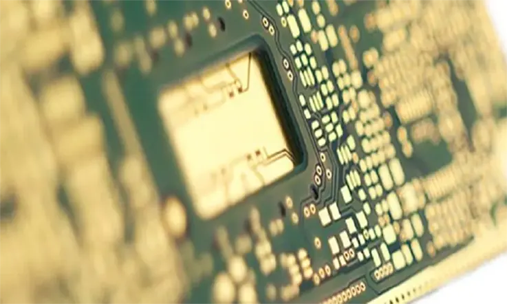
What are the Cavity PCB Components Assemble Technologies?
Implementing component assembly on cavity PCBs can engage a diversity of technologies and techniques, contingent on the distinct stipulations of the board and its application. Here are several of the prevalent technologies applied in cavity PCB component assembly:
Surface Mount Technology (SMT):
Surface-mount technology is a ubiquitous method employed in the assembly of components on cavity PCBs. With SMT, components are affixed directly onto the surface of the board. The attachment is executed by utilizing solder paste, followed by a reflow oven to secure the components to the board.
Through-hole Technology:
Through-hole technology encapsulates the practice of perforating component leads or pins through apertures in the board, succeeding which they are soldered to the contra side. This method, though not as frequently employed for cavity PCBs, might be requisite for specific applications or components.
Flip-chip Technology:
Flip-chip technology encompasses the procedure of affixing components directly to the board’s surface, with the contact pads oriented downward. Such a technique can result in enhanced electrical performance and thermal control, albeit necessitating specialized machinery and skillset.
Wire Bonding:
Wire bonding represents the technique of utilizing a thin wire to establish a connection between the component and the board via a bonding pad. This practice is predominantly leveraged for linking integrated circuits (ICs) and other miniature components.
Die Attach:
Die attach methodology entails mounting an unencased semiconductor die directly onto the board deploying a specialized adhesive. This tack is frequently adopted for high-power and high-frequency applications, in scenarios where a packaged component could potentially engender unfavorable parasitic phenomena.
Consequently, the selection of component assembly methodology for cavity PCBs hinges upon the specific requirements of both the board and its application. Accordingly, the manufacturer has to meticulously assess the design and materials that constitute the board to ascertain the most suitable assembly technology.
What is Cavity PCB Edge Plating?
Edge plating in cavity PCB involves a plating method where a metal layer is added to the exposed edges of the cavity on a printed circuit board. The main goal of edge plating is to enhance electrical connectivity, between the board layers and enhance themechanical stability of the board.
In a cavity PCB, the cavity is generally formed by eliminating a section of the board’s material, leaving to the exposure of the cavity’s edges. These edges can subsequently be coated with a slender layer of metal, which could be copper or gold employing potential techniques like electroplating or other comparable plating methods.
The process of edge plating offers advantages for cavity PCBs, such as:
●Improved electrical connectivity
●Increased mechanical stability
●Enhanced thermal management
Cavity PCB edge plating is a specialized process that requires careful attention to detail and precise control of the plating parameters. Despite these complexities, when performed accurately, this process can offer substantial advantages pertaining to the efficiency and dependability of cavity PCB.
Is Laser Technology Applicable for Cavity PCB?
In fact, laser technology finds wide application in the production process of cavity PCB. It can serve manifold purposes in the manufacture of cavity PCB, such as perforating holes or vias, fashioning circuit patterns, and extracting surplus material near the cavity.
Laser drilling is a prevalent technique for via creation in cavity PCB, permitting the precise drilling of minute holes swiftly and accurately. This method can be particularly efficacious in the creation of blind or buried vias to establish a connection with the board’s inner layers.
Laser cutting is a tool that can be employed to creating intricate circuit patterns, which can help to reduce the board’s overall size and weight. This can be particularly beneficial in applications where compactness is essential, like in mobile devices or wearable tech.
Furthermore, laser technology may also be used for excess material elimination around the cavity, improve thermal dissipation and mitigating the risk of component breakdown due to overheating.
In conclusion, laser technology can serve as a valuable tool in the manufacturing progression of cavity PCB, offering heightened precision, speed and flexibility in the fabrication process.
Future Developments and trends in Cavity PCB Technology
Cavity PCB techniques are ceaselessly advancing to meet the needs of contemporary electronics. Following are the anticipated advancements and directions in the domain of cavity PCBs:
The rise in 3D printing; It’s clear that more and more people are turning to printing for creating cavity PCB. As a result 3D printing is gaining traction as a favored method, for manufacturing cavity PCB.
Miniaturization: An escalating demand for tinier and more compact electronic gadgets is propelling the trend towards the diminution of cavity PCB. This trend is anticipated to persist, giving rise to even more intricate and condensed cavity structures.
Collaboration with emerging technologies: Cavity PCB are predicted to amalgamate more tightly with other progressive technologies, including artificial intelligence, Internet of Things, and 5G networks. This integration is forecasted to expedite the creation of novel applications and utilization instances for cavity PCB.
Higher operating frequencies: With the incessant expansion of demand for speedier and more efficient electronic gadgets, the necessity for cavity PCB to function at escalated frequencies becomes increasingly paramount. This will necessitate the genesis of development materials and fabrication techniques to support these higher frequencies.
Improved thermal management: Thermal management serves as an essential element influencing the functionality and dependability of cavity PCB. There is an unbroken investigation towards employing new materials and configurations to enhance thermal dispersal and curtail the probability of superheating.
Eco-technology: A burgeoning requirement for ecologically considerate electronic apparatus is fueling the progression of cavity PCB, incorporating sustainable materials and production methodologies.
Thus, the outlook for cavity PCB technology is promising, contemplating enduring innovation and progression anticipated to propel new applications and instances of usage for these particularized PCB.
In a Word
Cavity PCB distinguish themselves as a specific types of printed circuit boards that incorporate a cavity construct within the board. This cavity framework optimizes thermal dissemination, cuts down on size and weight, and improved signal quality, marking them optimal for a wide array of uses across multiple sectors.
When designing a cavity PCB it’s important to take into account factors such as the cavitys size and shape component placement, signal integrity, thermal considerations and manufacturing requirements. Cavity PCB are compared to types of PCB, like single layer, double layer and multi layer boards based on the specific needs of the application.
The onward trajectory of cavity PCB technology is forecasted to experience incessant advancements and evolution, with trends tilting towards compactness, elevated operating frequencies, improved thermal management, and amalgamation with other burgeoning technologies.
Consequently, cavity PCB extend distinctive merits and gains that render them a compelling choice for an extensive range of uses in diverse sectors.
Related Posts:
1.How to Build a Heater PCB Circuit Boards?
2.What is a Round Printed Circuit Board (PCB)?
3.Waterproof PCBs: Everything You Should Know