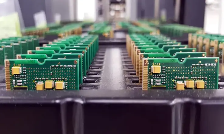
Over the past few years, the field of PCB development has witnessed significant advancements. From traditional boards for basic component integration, we have now moved towards circuit boards with complex components.
As PCB designers and manufacturers, we continuously strive to overcome challenges and achieve superior outcomes. Our goal is to provide innovative solutions and breakthroughs for various problems. In certain cases, these challenges may necessitate the development of new functionalities. This could involve a decision between a module-based or custom PCB design. In all such instances, specialized PCB types become indispensable. The ever-increasing demand to incorporate high-speed or high-power electronic capabilities into unconventional spaces has made special circuit board types crucial.
It is natural to have concerns and reservations when it comes to these specialized PCB. However, the success of PCB assembly and fabrication ultimately hinges on collaborating with the right contract manufacturer. To gain a comprehensive understanding of what constitutes a special PCB, it is essential to first define PCB board based on their mechanical and electrical properties. This knowledge will enable you to accurately define your board requirements. Additionally, we will explore how the manufacturing process of printed circuit boards using special materials can impact turnaround time and cost.
What is a Special PCB?
A Special PCB, alternatively referred to as a specialized or bespoke PCB (Printed Circuit Board), pertains to a category of circuit boards engineered and produced precisely for certain applications or requirements exceeding the usual PCB formats. These distinct PCBs are customized to accommodate the singular demands of specific trades, technologies, or environmental circumstances.
In contrast to conventional PCBs often found in diverse electronic gadgets, special PCBs are meticulously designed to tackle particular challenge or offer superior functionality. They might use advanced materials, boundary-pushing designs, or unconventional features to boost performance, dependability, or the alignment with specific components.
Special PCBs could come in multiple types like flexible PCB, rigid-flex PCB, high-density interconnect (HDI) PCB, metal core PCB, High TG PCBs, among others. Each special PCB types fulfills a dedicated function and finds its usage in precise scenarios where the conventional PCBs might not prove adequate.
The design and manufacturing of special PCBs require expertise in understanding the specific requirements, constraints, and technical considerations of the intended application. This may involve selecting suitable materials, incorporating special signal routing techniques, implementing thermal management solutions, or ensuring compliance with industry standards and regulations.
Overall, special PCBs play a crucial role in enabling the development of advanced electronic systems, devices, and technologies that require tailored circuit board solutions to meet the demanding needs of specific industries or applications.
Special PCB Types and Application
Special PCBs include different varieties engineered to cater to distinct needs and use-cases. The following are some prevalent types of special PCBs:
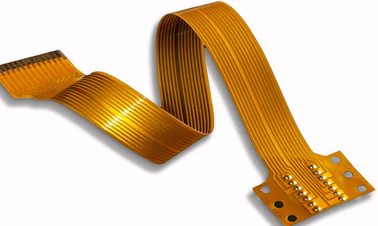
Flexible PCB:
Comprised of pliable materials such as polyimide or polyester, these PCB board have the ability to bend, twist, or adapt to uneven surfaces. They are perfectly suited for applications demanding compact, lightweight and bendable circuits. Such as in wearable devices, medical apparatus and aerospace systems.
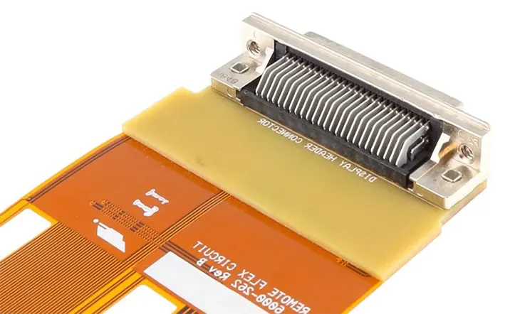
Rigid-flex PCB:
By integrating the features of both rigid and flexible PCB, these boards comprise rigid components linked by flexible circuits. This provides a flexible approach to intricate electronic assemblies. Rigid-flex PCB are commonly used in devices with folding or bending mechanisms, like smartphones, digital cameras and portable electronics.
High-Density Interconnect (HDI) PCB:
HDI PCB are designed to accommodate a high number of components and interconnections in a compact form factor. They employ sophisticated microvia technology, intricate traces and numerous layers to realize high circuit density. Predominantly, HDI PCB are found in compact electronic devices. For example smartphones, tablets and other microelectronics.
Metal Core PCB:
Metal core PCB have a layer of thermally conductive material, typically aluminum or copper, as the base layer. Their exceptional heat dispersion properties make them ideal for high-power applications which engender substantial heat, including LED lighting, power electronics and vehicle components.
High-Temperature PCB:
High-temperature PCB are designed to withstand elevated temperatures without compromising performance or reliability. They utilize specialized materials with high glass transition temperatures and low thermal expansion coefficients. These PCB are used in applications such as automotive engine control units, aerospace systems, and industrial equipment operating in harsh environments.
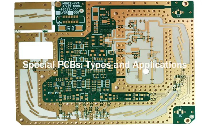
RF/Microwave PCB:
RF (Radio Frequency) and microwave PCB are optimized for high-frequency signal transmission and minimal signal loss. They feature specific trace geometries, controlled impedance, and low dielectric constant materials to maintain signal integrity. RF/Microwave PCB are crucial in wireless communication systems, radar systems, satellite technology and high-speed data applications.
Hybrid PCB:
Hybrid PCB combine different technologies or materials to achieve specific functionalities. For example, a hybrid PCB might integrate traditional rigid PCB sections with flexible PCB sections to combine the benefits of both. Hybrid PCB are used in applications that require a combination of rigid and flexible elements, such as automotive control systems and complex industrial machinery.
These are just a few examples of special PCB types. Depending on the specific requirements and industry, there can be additional specialized PCB variants developed to meet unique application needs.
Design Considerations for Special PCBs
Designing special PCBs requires careful consideration of various factors to ensure optimal performance and functionality. Here are some common design considerations for special PCBs:
Material Selection: Choose appropriate materials based on the specific requirements of the special PCB. Consider factors such as dielectric constant, thermal conductivity, mechanical strength, and chemical resistance. Special materials like flexible substrates, high-temperature laminates, or metal core laminates may be required for specific applications.
Thermal Management: Special PCBs often handle high-power components or operate in environments with elevated temperatures. Implement effective thermal management techniques such as heat sinks, thermal vias, and copper pours to dissipate heat and maintain proper operating temperatures.
Signal Integrity and EMI/EMC: Special PCBs may have stringent signal integrity requirements. Consider signal integrity issues such as impedance matching, controlled impedance traces, and minimizing signal reflections. Implement proper grounding techniques and utilize shielding to mitigate electromagnetic interference (EMI) and ensure electromagnetic compatibility (EMC).
High-Density Design: Special PCBs may require accommodating a high density of components and traces. Optimize component placement and routing to minimize signal crosstalk, maintain clearances, and ensure proper signal integrity. Utilize advanced design techniques like blind and buried vias, microvias, and HDI (high-density interconnect) technologies.
Mechanical Constraints: Some special PCBs may need to conform to specific mechanical requirements. Consider factors such as size and form factor, mounting or attachment mechanisms, and structural integrity. Design the PCB to withstand mechanical stresses, vibrations, and environmental conditions.
Manufacturing and Assembly Challenges: Special PCBs may involve unique manufacturing processes and assembly considerations. Collaborate closely with manufacturers to ensure the design can be feasibly manufactured. Consider factors such as fabrication capabilities, assembly techniques, and any specific design rules or constraints imposed by the manufacturing process.
Reliability and Testing: Special PCBs often require high reliability. Perform thorough design verification and testing to ensure the PCB meets the desired performance criteria. Consider environmental testing, stress testing, and any specific reliability standards applicable to the intended application.
Cost Optimization: Balance the design requirements with cost considerations. Optimize the design to minimize the overall manufacturing and assembly costs while still meeting the desired specifications and performance criteria.
It’s crucial to acknowledge that these considerations function as basic guidelines, and the specific design contemplations might fluctuate based on the kind of unique PCB and its designated utilization. Hence, seeking advice from experts or specialized PCB designers adept in the particular type of unique PCB you are handling is recommended.
How to Optimize Special PCB Board Manufacturing Process?
Optimizing the production process for distinct PCB boards calls for thorough evaluation of diverse factors to guarantee productive fabrication and premium results. Below are some suggestions to optimizethe manufacturing process:
Design for Manufacturability (DFM):
Ensure that the PCB design is optimized for manufacturability. Collaborate closely with the manufacturer during the design phase to understand their capabilities, limitations, and preferred design guidelines. Consider aspects such as panelization, component placement, trace widths, and spacing to facilitate smooth manufacturing processes.
Material Selection:
Select materials that are easily obtainable and consonant with the manufacturing process. choose for materials presenting excellent dimensional constancy, excellent thermal attributes, and desirable electrical specifications for the. Work with the manufacturer to identify the most cost-effective and efficient material options.
Efficient Panelization:
Optimize the panelization of PCBs to peak the consumption of the raw material while reducing waste. Arrange the PCBs on the panel in a way that allows for efficient assembly and reduces the number of steps required in the manufacturing process. Contemplate factors such as panel dimension, gap, fiducial markers, and tooling orifices.
Component Management:
Streamline component management processes to avoid delays and errors. Maintain accurate component libraries and ensure that the Bill of Materials (BOM) is up to date. Implement effective inventory management practices to prevent shortages or excess stock. Consider automation tools for component placement and verification to improve efficiency and accuracy.
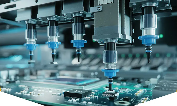
Automated Assembly:
Utilize automated assembly processes wherever possible to improve efficiency and reduce human error. Automated processes such as pick-and-place machines, solder paste deposition, and reflow ovens can significantly speed up assembly while maintaining consistency and quality.
Quality Control and Testing:
Institute stringent quality management protocols throughout the production procedure. Perform regular inspections, testing, and verification to identify and address any manufacturing defects or issues early on. Implement statistical process control techniques to monitor and improve process performance over time.
Documentation and Communication:
Maintain clear and detailed documentation of the manufacturing process, including work instructions, process flowcharts, and quality standards. Foster effective communication channels between the design team and the manufacturing team to address any design-related issues or concerns promptly.
Continuous Improvement:
Continuously evaluate and improve the manufacturing process based on feedback, lessons learned, and industry best practices. Solicit feedback from the production crew and integrate their perspectives into forthcoming design revisions. Periodically scrutinize and refine the manufacturing methodology to bolster productivity, diminish wastage, and escalate the overall quality.
Collaboration with Manufacturing Partners:
Formulate a robust association with the PCB manufacturer, perpetuating an open channel for communication. Involve the manufacturer early in the design process to leverage their expertise and ensure that the design aligns with their manufacturing capabilities.Maintain consistent collaboration to tackle any manufacturing difficulties and challenge.
Abiding by these rules and working intimately with the PCB manufacturer will enable you to refine the special PCB board manufacturing procedure, facilitating effective production, cost reduction, and the delivery of top-tier products.
Considerations for Choosing a Manufacturer for Your Special PCB
Identifying the appropriate manufacturer for your specific PCB is instrumental to securing the successful fabrication of superior quality boards that abide by your specialized needs. Below are some factors to cater to when pinpointing a manufacturer:
Expertise and Experience: Seek out a manufacturer possessing expertise and experience in creating special PCBs. Evaluate their history and probe into their proficiency in producing PCBs akin to your explicit needs. A manufacturer fortified with specialized understanding and experience will be better prepared to tackle the unique challenge of your PCB project.
Manufacturing Capabilities: Evaluate the manufacturer’s capabilities and facilities. Consider factors such as their production capacity, equipment, and technology capabilities. Ensure that they have the necessary equipment and processes required for manufacturing your special PCB, including any specialized technologies or techniques.
Quality Control and Certifications: Quality control is crucial for special PCBs. Assess the manufacturer’s quality control processes, certifications (such as ISO 9001), and adherence to industry standards. Inquire about their inspection and testing procedures to ensure that rigorous quality checks are performed throughout the manufacturing process.
Design for Manufacturability Support: Collaborative support during the design phase is essential. Choose a manufacturer that can provide design for manufacturability (DFM) feedback and guidance. They should be able to review your design, identify any potential manufacturing issues, and suggest improvements to optimize manufacturability and avoid costly errors.
Material Selection and Sourcing: Check whether the manufacturer is equipped with a broad array of materials apt for your unique PCB. They should maintain well-founded partnerships with dependable material suppliers, guaranteeing the accessibility of superior quality materials. Inquire their material selection process and determine whether they can adapt to your particular material requisites.
Prototyping and Small Batch Production: Should your needs encompass prototyping or small scale production, verify that these services are within the manufacturer’s offerings. They ought to display the flexibility and eagerness to collaborate with you during the prototyping phase, permitting iterations and modifications prior to transitioning into full-blown production.
Supply Chain Management: Evaluate the manufacturer’s supply chain management capabilities. Consider factors such as their ability to source components, manage inventory, and handle logistics efficiently. A well-managed supply chain will help ensure timely delivery of components and minimize production delays.
Communication and Support: Effective communication and support are critical for a successful manufacturing partnership. Assess the manufacturer’s promptness, communication avenues, and their ability to offer timely progress reports of your task. Choosing for a manufacturer ready to work hand-in-hand, and is quick to address any challenges or hindrances that could surface during the manufacturing course.
Cost and Pricing: Although cost is a significant factor, it shouldn’t be the only criterion driving the decision. Assess the pricing models of various manufacturers, factoring in elements like quality, technical competence, support and added-value services. select for a manufacturer who presents a just equilibrium between cost and quality.
References and Reviews: Seek references and reviews from other customers who have worked with the manufacturer. Feedback from previous clients can provide valuable insights into their reliability, quality, and overall performance.
By carefully considering these factors and conducting thorough research, you can select a manufacturer that aligns with your specific requirements, ensuring a successful and efficient production process for your special PCBs.
Importance of Special PCBs
Special PCBs play a crucial role in various industries and applications due to their unique characteristics and tailored designs. Here are some key reasons highlighting the importance of special PCB:
Customization: Special PCBs offer customization options to meet specific requirements. They can be designed to accommodate complex circuitry, unique form factors, and specific functionality that cannot be achieved with standard PCBs. This customization allows for optimized performance and integration within the targeted application.
Enhanced Performance: Specialty PCBs are design to proffer superior functionality in comparison to typical PCBs. They can offer heightened signal integrity, cut down on noise, offer increased power endurance, and advance thermal management. These performance augmentations are of utmost importance in applications where dependability, accuracy, and efficiency are cardinal.
Harsh Environment Compatibility: Special PCBs are designed to withstand challenging environmental conditions. They can be built to resist high temperatures, extreme humidity, vibrations, shock, and exposure to chemicals or corrosive substances. Such resilience ensures the reliable operation of electronic systems in demanding industries like aerospace, automotive, and industrial automation.
Miniaturization and Integration: Many special PCB are tailored to bolster miniaturization endeavors, empowering a denser packaging of electronic elements. They facilitate the production of small-scale devices and systems whilst upholding their full capacity. This is especially prominent in industries like consumer electronics and medical appliances, where size and portability are essential.
Specialized Applications: Certain industries necessitate PCBs with unique features and functions, customized for their distinct applications. Special PCBs cater to these particular requirements, including flexible PCB for bendable or curved applications, high-frequency PCB for wireless communication structures, or high-density interconnect (HDI) PCB for environments with limited spacing. These specific applications lean on special PCBs to attain peak performance and functionality.
Reliability and Durability: Special PCB are subjected to a stringent design and testing process to guarantee top-level trustworthiness and longevity. They are assembled using advanced materials, cutting-edge fabrication techniques and rigorous quality check. This dependability is paramount in essential applications like medical instruments, aerospace systems and industrial controls, where system malfunctions could lead to disastrous outcomes.
Innovation and Advancements: Special PCB are pioneers in numerous sectors driving innovation. They facilitate the evolution of breakthrough technologies such as advanced driver assistance systems (ADAS) in the automotive industry, high-speed data dissemination in telecommunications, and scaled-down medical implants. Special PCB serve as the bedrock for technological progress, continually expanding the realm of feasibility.
Which Technologies Used in Special PCB Manufacturing?
HDI Blind Buried Hole:
Blind vias, identifiable solely on the top or bottom layers of a Printed Circuit Board (PCB), are generally created from the board’s surface. In contrast, buried vias are within the inner layers of the PCB. These via types are primarily drilled in the internal layers, which underscores their categorization as internalized circuit-board holes. The adoption of blind and buried vias has markedly elevated the quality and dimensions of High-Density Interconnect (HDI) PCBs. These vias additionally boost electromagnetic compatibility, slim down layer count, streamline PCB design, and curtail expenses.
The integration of blind buried hole technology has reached its pinnacle in FR-4 prototypes with up to 20 layers. These prototypes feature a board thickness of ≤6.0mm, and blind holes spanning stages 1 to 4, utilizing laser drilling technology.
Multi-Layer Special Stack-Up Structure:
The growing necessity for high-velocity circuits has escalated the intricacy of PCB boards. In order to curb electrical disturbances, it becomes essential to separate the power layer from the signal layer. As a result, this operation employs a multi-layered approach.
Furthermore, the stack-up structure plays a crucial role in the electromagnetic compatibility (EMC) performance of circuit boards, serving as a critical measure to reduce electromagnetic interference. When the device density is higher, the PIN density of signal networks also increases. In such cases, a special stack-up structure becomes imperative.
Impedance Control:
Characteristic impedance refers to the resistance encountered by electromagnetic waves or high-frequency signals during transmission along the signal lines of components. The PCB’s characteristic impedance value must correspond to the electronic impedance of the tail and head components to ensure proper transmission of digital signals on the circuit board.
Mismatched impedance results in signal reflection, delay, attenuation, and scattering of transmitted signal energy. Therefore, PCB designers must implement impedance control. Impedance control can be achieved in FR-4, flexible circuit boards, and rigid-flex boards, allowing for 2 to 20 layers.
Thick Copper PCB:
Thick copper PCB are a type of printed circuit board with a copper thickness of 2 oz or greater. These PCB possess properties such as corrosion resistance, low-temperature resistance, high-temperature resistance, and excellent expansion performance. These attributes contribute to increased lifespan and simplified size of electronic devices. Some PCB designers can achieve 2 to 6 layers using thick copper PCB technology, with 10 oz being the maximum copper thickness.
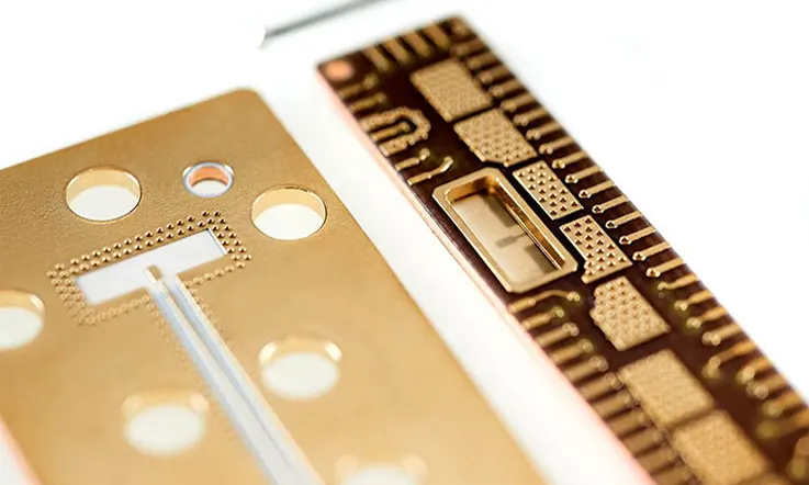
Electroless Nickel Electroless Palladium Immersion Gold (ENEPIG):
ENEPIG is a commonly used surface finish type in circuit boards. The ENEPIG process involves depositing nickel, palladium, and gold on the PCB surface using chemical methods. This surface finish technology is non-selective.
ENEPIG integrates a 50 nm thick palladium plating and a 10 nm thick gold plating. This integration provides anti-friction properties, corrosion resistance, and good electrical conductivity. The appearance and physical properties mentioned above can be influenced by the thickness of the copper layer. ENEPIG represents the latest surface finish technology integrated into PCB prototypes.
Electroplated Nickel Gold/Gold Finger
Electroplated nickel gold, also called electrolytic gold is a surface finishing method where gold particles are bonded to the circuit board using electroplating. It is often known as hard gold because of its excellent adhesion characteristics.
This process bolsters the resistance to wear and the hardness of the circuit board, all the while curbing the spread of copper and alternate metals. It is also compliant with the specifications for soldering and thermal bonding. The resulting coating features admirable malleability, minimal strain, and low porosity. As a result, this specific layer is extensively applied in the realm of PCB proofing.
Conclusion
Special PCB cater to unique needs, offering notable benefits across a range of industries and applications. This artcle delves into several types of these special PCB like flexible PCB, rigid-flex PCB, HDI PCB, metal core PCB, and high-temperature PCB and so on.
In the course of the design procedure, numerous critical elements have been accentuated. These encompass material choice, thermal administration, signal integrity and EMI/EMC, high-density layout, mechanical restrictions, fabrication and assembly hurdles, dependability, testing, and cost efficiency. Addressing these determinants guarantees that the specially-designed PCB satisfy the specific requirements of their intended applications.
It is important to note that designing special PCB requires expertise and collaboration between designers, manufacturers, and industry professionals to ensure successful implementation. By comprehending the singular traits, challenge, and prospects related to these specialized PCB, engineers have the capability to devise revolutionary solutions that boundaries the limits of technology and propel progressions in diverse industries.
In essence, special PCB play a crucial role in enabling advanced functionalities and meeting the evolving needs of modern industries. Amidst continuing exploration and advancements, we anticipate witnessing further advancements and applications of these distinct PCB in forthcoming times, thus contributing significantly to technological progress and innovation.
Related Posts:
1.How to Build a Heater PCB Circuit Boards?
2.What is a Round Printed Circuit Board (PCB)?