This article provides a comprehensive explanation of hybrid printed circuit boards, outlining their concept and functioning. Hybrid PCB are designed to optimize the benefits they offer to end users by integrating multiple technologies. This unique design incorporates ceramic, rigid, and flexible PCB materials, allowing the utilization of components that are typically incompatible when used on a single-material board. Below, we address some frequently asked questions regarding this subject to enhance understanding.
What is Hybrid PCB?
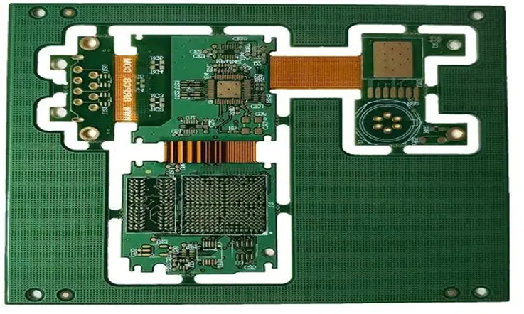
A hybrid PCB, short for hybrid printed circuit board, is a specialized type of circuit board that combines multiple technologies and materials to maximize its functionality and compatibility with various components. In contrast to orthodox PCBs that are fashioned out of a solitary material, hybrid PCBs encompass an assortment of substances, such as ceramic, rigid, and flexible substrates into an individual board. This strategy facilitates the inclusion of components that might otherwise be unsuitable for a standard PCB. The hybrid blueprint empowers the board to fulfill designated requisites, deliver improved efficiency, and host an expanded array of electronic elements, thereby offering a versatile resolution for intricate electronic systems.
Why are Different Materials Used for Designing Hybrid PCB?
Hybrid Printed Circuit Boards are architected utilizing diverse substances to address particular necessities and enhance the function of the electronic apparatuses they’re incorporated in. Here, we’ll explore the reasons behind the use of varied materials in hybrid PCB design:
Substrate Selection:
The selection of substrate matter in a hybrid PCB is dictated by its electrical, thermal, and mechanical attributes. Dissimilar substances grant diverse degrees of electrical insulation, thermal conductivity, rigidity, and dimensional constancy. To illustrate, FR-4 is a frequent substance employed that bestows excellent electrical insulation as well as strong mechanical robustness.
Component Placement:
Frequently, hybrid PCBs incorporate a mix of surface-mounted alongside through-hole constituents. The opting for materials in diverse sections of the PCB assists in housing and securing these elements effectually. For example, certain zones of the PCB might necessitate a heightened glass transition temperature (Tg) to endure the warmth produced by surface-mounted constituents.
Signal Integrity:
The materials used in hybrid PCB impact the signal integrity and transmission characteristics of high-speed signals. For high-frequency applications, materials with low dielectric constants and low loss tangents are preferred to minimize signal distortion and maintain signal integrity.
Thermal Management:
Hybrid PCB may have components that generate significant heat during operation. In order to distribute heat proficiently and avert overheating, materials possessing superior thermal conductivity are employed. As a case in point, metal core PCB incorporate a metal core, like aluminum or copper, to equip efficient heat dispersion.
Environmental Considerations:
Depending on the application and operating conditions, the PCB could be prone to harsh environments, encompassing heavy moisture, severe temperatures, or chemical contact. Under such circumstances, materials exhibiting strong moisture resistance, temperature steadiness, and chemical resistance are selected to affirm the durability and dependability of the PCB.
Cost Optimization:
The choice of materials also considers cost optimization. Certain applications might necessitate costly high-end materials, while others might favor more budget-friendly alternatives that satisfy the required specifications.
Worth mentioning is the fact that material selection for hybrid PCB design is intricate and necessitates the evaluation of multifarious factors like electrical needs, thermal management, signal propriety, dependability, and cost. Designers are obligated to prudently assess these elements and select suitable materials to actualize the aimed performance and functionality of the hybrid PCB.
Materials Utilized in the Fabrication of Hybrid PCB
The manufacturing of hybrid PCB necessitates the use of diverse materials to effectuate the required performance and compatibility. Some of the cardinal materials frequently employed in the assembly of hybrid PCB consist of:
Ceramic Substrates: Ceramic substances, such as alumina (Al2O3) or aluminum nitride (AlN), are commonly harnessed in the realm of hybrid PCB. These ceramic substrates boast sterling thermal conductivity, electrical insulation parameters and lofty mechanical resilience, rendering them beneficial for components that generate a considerable degree of heat.
Rigid Substrates: Rigid materials, such as epoxy-based laminates (FR-4), are frequently incorporated into hybrid PCB. Rigid substrates gift the board with structural reinforcement and steadiness, permitting standard electronic component mounting and smoothening the fabrication procedure.
Flexible Substrates: Flexible materials, like polyimide or polyester, are used in hybrid PCB to achieve flexibility and bendability. Flexible substrates empower the board to mold to irregular contours, nestle into confined spaces, and endure mechanical strain, notably beneficial in applications where space is scarce or repetitive bending is necessary.
Conductive Materials: Hybrid PCB deploy conductive entities like copper for the traces and vias to establish electrical connections among various components and circuit elements. Copper is championed owing to its high conductivity, trustworthiness, and compatibility with assorted manufacturing procedures.
Through the integration of these diverse materials within a singular PCB, hybrid designs can harness the advantages of each material to boost performance, manage thermal properties and correlate with a broad spectrum of components, eventually amplifying the overall capability and reliability of the electronic system.
Features of hybrid PCB
Hybrid PCB present numerous significant attributes that render them a favored option in an array of electronic applications. Some principal characteristics of hybrid PCB entails:
Material Compatibility: A direct standout feature of hybrid PCBs is their capacity to amalgamate an assortment of materials, including ceramic, firm, and malleable substrates, onto one consolidated board. This allows for the integration of components that would not typically be compatible on a traditional PCB, expanding the range of possibilities for electronic system design.
Component Integration: Hybrid PCB enable the integration of diverse components, including those with different form factors, technologies, or specialized requirements. By accommodating a wide variety of components on a single board, hybrid designs offer flexibility and efficiency in system assembly and mitigating the need for supplemental interconnections or intricate wiring arrangements.
Enhanced Functionality: The integration of varied materials and an array of component types in a hybrid PCB supremely elevates the overall operational capability of the electronics system. It permits the inclusion of components with definitive properties like high-capacity instruments, sensors, or adaptive displays, substantially broadening the system’s functioning potential.
Space Optimization: Hybrid PCB can optimize space utilization within electronic systems. By integrating components that may have different size or shape requirements, hybrid designs can effectively utilize available space and reduce the overall footprint of the system. This is particularly advantageous in compact devices or applications with limited space.
Thermal Management: The use of ceramic substrates in hybrid PCB provides excellent thermal conductivity, allowing for efficient heat dissipation. This characteristic proves advantageous for components that emit substantial quantities of heat, securing their accurate operation which in turn escalates the dependability and duration of the electronic mechanism.
Design Flexibility: Hybrid PCB provide designer greater flexibility in terms of layout and circuit design. The incorporation of different materials and component types allows for creative and optimized designs that meet specific performance requirements and overcome design constraints.
The Downsides to the Hybrid PCB
Complexity: Hybrid PCB involve the integration of dissimilar materials, which can increase the complexity of the design and manufacturing processes. Working with multiple materials requires expertise in handling and processing each material, leading to additional challenges in terms of design, fabrication and assembly.
Cost: While cost optimization is a potential benefit of hybrid PCB, a significant balance must be struck between the inclusion of high-priced and cost-effective materials. At times, the cost of incorporating dissimilar materials and the associated manufacturing processes can outweigh the benefits gained from their selective use. The cumulative price of hybrid PCBs might surpass that of conventional PCBs due to specified necessities and heightened sophistication.
Manufacturing Challenges: Hybrid PCB often require specialized manufacturing techniques and equipment to accommodate the different materials used. This can lead to longer lead times, increased production costs, and potential difficulties in finding suitable fabricators with the necessary expertise.
Reliability: The integration of dissimilar materials in hybrid PCB introduces potential reliability concerns. Different materials may have varying coefficients of thermal expansion (CTE), which can result in mechanical stress and potential failure at the junctions between these materials. Thorough analysis and design considerations are required to minimize the risk of reliability issues.
Design Limitations: Hybrid PCB may impose certain design limitations due to the incorporation of dissimilar materials. Specific material properties, such as dielectric constant and thermal conductivity, can affect signal integrity and thermal management. Designers must carefully consider these limitations and optimize the layout and routing accordingly.
Testing and Inspection: Hybrid PCB may require specialized testing and inspection methods to ensure the integrity of the different materials and interfaces. This can add complexity and additional costs to the quality assurance process.
Although accompanied by certain drawbacks, hybrid PCB persistently provide exclusive benefits for particular applications demanding a blend of diverse material characteristics. It remains crucial to meticulously scrutinize the project’s necessities and contemplate the balance between the virtues and challenges prior to deciding on the utilization of hybrid PCB technology.
Designing Hybrid PCB: Essential Materials and techniques for Consideration
In the designing process of a hybrid Printed Circuit Board, numerous materials and techniques necessitate consideration for achieving foremost performance. A Hybrid PCB embodies attributes of both rigid and flexible circuits, promoting enhanced operationality and adaptability. Here are a number of materials and techniques one should bear in mind during the design stage of a hybrid PCB:
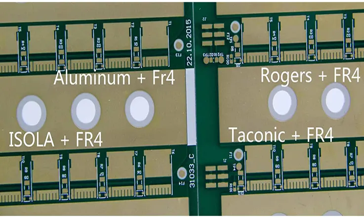
Substrate Materials: The substrate material used in a hybrid PCB can be a combination of materials like FR-4, polyimide and Rogers. The selection of substrate materials depends on the application requirements such as cost, thermal management, and electrical performance.
Layer Stack up: The layer stack up of a hybrid PCB can be customized according to the design requirements. A hybrid PCB allows for the integration of both rigid and flexible layers. The stack up design should ensure signal integrity, minimize signal loss, and provide thermal management.
Copper thickness: Copper thickness plays a pivotal role in the design of a hybrid PCB. Depending on the specific application, the copper Thickness on a hybrid PCB can fluctuate, ordinarily lying within the range of 0.5 oz to 2 oz.
Via Types: The via types used in a hybrid PCB can be of different types, including through-hole, blind, buried, and microvias. The via types used should be selected according to the application requirements.
Surface Finish: The surface finish used in a hybrid PCB can be of different types, including HASL, ENIG, OSP and Immersion Tin. The surface finish should be selected according to the application requirements.
Design for Manufacturing (DFM): DFM is an essential consideration when designing a hybrid PCB. The design should take into account the manufacturing process, such as the panelization, tooling holes, and fiducial marks.
To sum up, designing a hybrid PCB requires careful consideration of materials and techniques to ensure optimal performance. The substrate materials, layer stack-up, copper thickness, via types, surface finish, and DFM are all important factors to consider when designing a hybrid PCB.
When Should Hybrid PCB Stack Up be used?
Factors determining the use of hybrid PCB encompass various considerations, such as costs, temperatures, application functions, and frequencies. Embracing hybrid PCB stack ups offers the advantage of enhancing creativity during circuit board fabrication, enabling the attainment of desired mechanical and electrical properties.
Cost considerations play a pivotal role in hybrid designs. By employing dissimilar materials, cost optimization becomes feasible. Economical materials can be utilized in sections where higher frequencies are unnecessary, while expensive materials can be judiciously allocated to areas requiring enhanced electrical, thermal, and mechanical properties.
Mechanical Features of a Hybrid PCB:
Mechanical features of hybrid PCB present unique challenges during fabrication. Notably, odd-shaped board outlines demand meticulous routing to ensure seamless integration within the available space. This entails reducing speeds and feeds to maintain crisp edges. Additionally, careful monitoring of drill bits becomes imperative due to the complexity of the materials involved, as certain RF materials are prone to fraying if not appropriately cut.
Plated through hole consistency:
Maintaining consistency in plated through holes is another important aspect. Fabricators must recognize the distinct hole preparation requirements for FR-4, as compared to other materials. Understanding the impact of these processes on hole wall quality is crucial, as plasma etching is commonly employed to desmear PTFE holes but can result in uneven surfaces and subsequently uneven copper deposition in FR-4 holes.
Controlled depth rout process:
Controlled depth routing processes contribute to the mechanical features of hybrid PCB. Some features arise from multiple lamination cycles, while others stem from the implementation of controlled-depth routing patterns. However, these processes introduce complexities and costs to the PCB design. Manufacturers must skillfully rout out patterns in the prepreg and the production pattern when utilizing multiple lamination cycles to create cavities.
All in all, the mechanical features of hybrid PCB necessitate careful attention and expertise during fabrication. Achieving precise odd-shaped board outlines, ensuring plated through hole consistency, and navigating controlled depth routing processes require specialized knowledge and meticulous execution to deliver high-quality hybrid PCB.
Applications of hybrid PCB
Hybrid PCB are employed across a diverse spectrum of sectors, attributed to their singular amalgamation of material attributes and improved design faculties. Here are a few conventional employments of hybrid PCB:
Aerospace and Defense:
Hybrid PCBs are abundantly utilized within the aerospace and defense segments due to their resilience against severe environments, elevated heat, and intense vibrations. The fusion of distinct materials such as PTFE and ceramics enables the fabrication of robust and reliable PCBs, capable of operating under demanding conditions.
Telecommunications:
Hybrid PCB are ideal for high-frequency applications that require superior signal integrity and thermal management. By incorporating specialized materials such as Rogers and ceramic substrates, hybrid PCB can achieve exceptional electrical performance and thermal stability, making them a preferred choice for telecommunications applications.
Automotive:
The automotive industry relies on hybrid PCB for their ability to withstand high temperatures, vibrations, and moisture. Hybrid PCB can be designed to incorporate specialized materials such as aluminum-backed substrates, allowing for efficient thermal management and improved reliability.
Medical:
Hybrid PCB are also utilized in medical devices and equipment, thanks to their ability to incorporate specialized materials that offer high thermal stability and biocompatibility. These PCB can be design to endure processes such as autoclaving and sterilization, thereby making them optimally suited for utilization in medical equipment.
Industrial:
Hybrid PCB are typically employed in industrial usage demanding high dependability and durability. The integration of particular materials, such as ceramic bases and aluminum-backed PCB, renders hybrid PCB robust enough to resist severe environments, elevated temperatures, and intense oscillations.
Broadly speaking, hybrid PCB offer a versatile solution for applications that require a combination of material properties and enhanced design capabilities. Their ability to incorporate dissimilar materials enables the creation of PCB that can withstand demanding conditions, which makes them a perfect selection for a diverse array of sectors.
Conclusion
As a manufacturer in fabrication hybrid PCB, we pride ourselves on being among the top experts in the field. Our extensive experience equips us with the expertise required to deliver superior PCB designs that precisely align with your unique specifications. We persist in our devotion to quality, and employing cutting edge equipment and capitalizing on our rich manufacturing experiences to assure peak perfection across the entire design procedure.
By consigning us with your hybrid PCB demands, you can rest assured in acquiring customized solutions that exceed your anticipations. We understand the nuances associated with handling hybrid PCB, and our mastery allows us to traverse these complexities smoothly. With our comprehensive understanding of material integration and component selection, we ensure that your bespoke designs are executed flawlessly, meeting your specific needs and objectives.
Collaborating with us assures availment of our steadfast commitment to dispatching remarkable hybrid PCB designs and circuit boards. We prioritize precision, reliability, and innovation in every project we undertake. By leveraging our expertise and state-of-the-art equipment, we strive to exceed industry standards, providing you with the highest level of satisfaction.
Experience the advantage of working with professionals who excel in the realm of hybrid PCB. Contact us today to discuss your requirements, and let us demonstrate our commitment to delivering outstanding results tailored to your precise specifications.
Related Posts:
2.How Planning Stackup for Rigid-Flex PCB Circuit Board?
3.Rigid-Flex PCB Assembly Fundamentals and Operational Principles