
Modern electronics owe much of their functionality to printed circuit boards (PCBs), which serve as the foundation for devices ranging from basic household items to advanced medical instruments and communication systems. Among the array of PCB types, multilayer PCBs are especially valued for their capability to manage intricate circuitry while packing high performance into compact designs. Whether you’re a seasoned expert or just stepping into the world of PCBs, grasping the details of multilayer PCB design, manufacturing, and assembly processes can significantly enhance the efficiency and value of your projects. Buckle up, as mastering these details can help you take your projects from “meh” to “wow” without breaking a sweat.
Understanding the Basics: What is a Multilayer PCB?
Definition of Multilayer PCB: A Complex Circuitry Solution
In the world of PCBs, multilayer PCBs represent the top of the food chain, used for advanced, high-performance devices. Unlike single-layer or double-layer PCBs, which have just one or two copper layers, multilayer PCBs pack in three or more copper layers that are interspersed with insulating layers. Think of it like a sandwich, but way more high-tech: you’ve got the bread (insulation layers) and the filling (copper for signals and power). These layers are meticulously bonded together to form a compact, high-density structure that allows complex circuits to coexist in a small footprint.
When designing multilayer PCBs, precision is key. The interconnection between these layers requires vias (tiny drilled holes that are plated with copper) to connect different levels, making the whole thing work seamlessly. This structure allows signal integrity to be maintained, even at higher speeds, which is a massive deal in today’s digital world.
Types of Multilayer PCBs: Choosing the Right Design
Let’s break down the types of multilayer PCBs you’ll typically encounter. They all have their unique advantages depending on the specific needs of your application.
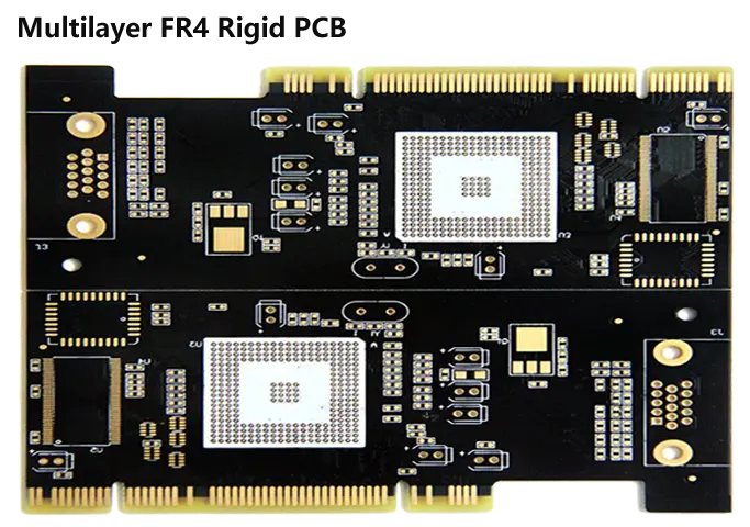
1.Rigid Multilayer PCBs-
This is your traditional workhorse. Made with a rigid substrate (often FR4), it’s designed for boards that need a solid structure. The rigid multilayer PCB is your go-to for most consumer electronics like smartphones, laptops, and automotive electronics. It’s solid, dependable, and can handle complex designs without breaking a sweat.
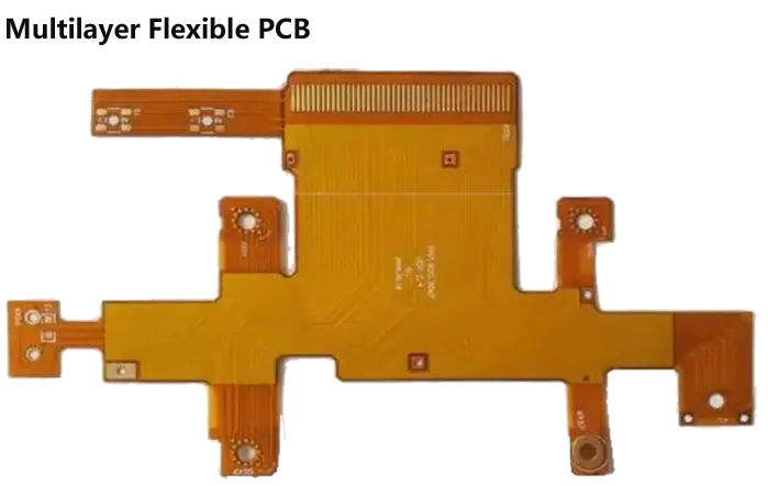
2.Flexible Multilayer PCBs-
Now we’re talking flexibility—literally. These PCBs are built on flexible substrates such as polyimide or Kapton, meaning they can bend and twist without falling apart. It’s perfect for applications where you need to cram in circuitry but also need flexibility, such as wearable tech, medical devices, or even foldable phones. The flexible nature allows them to be folded or rolled up without damaging the connections, which is pretty rad in today’s market.
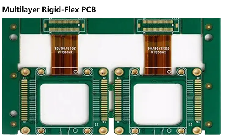
3.Rigid-Flex Multilayer PCBs-
Blending the rigidity of traditional PCBs with the adaptability of flexible circuits, rigid-flex PCBs deliver a hybrid approach that’s perfect for complex design challenges. These boards combine sturdy sections for mounting stable components with flexible areas that allow the board to bend or twist, making them a standout choice for applications like drones, wearables, and automotive systems. Picture a circuit that needs to wrap around a curved surface while maintaining durable, reliable connections in critical areas—rigid-flex technology handles this with finesse. Whether it’s surviving a drone crash or adapting to a smartwatch’s sleek design, this innovative solution offers the flexibility and durability to handle the demands of modern electronics.
Multilayer PCB Stackup: The Blueprint for Success
The stackup refers to how the layers of a multilayer PCB are arranged. This structure is what makes the magic happen. When you’re stacking up a multilayer PCB, you’re aiming for a perfect balance between signal integrity, power distribution, and grounding. Let’s break it down:
Typical Multilayer Stackup-
| Layer | Purpose | Material |
| Top Layer | Signal layer | Copper/FR4 |
| Ground Plane | Noise reduction | Copper |
| Power Plane | Power distribution | Copper |
| Signal Layer | Routing data signals | Copper/FR4 |
| Bottom Layer | Signal layer | Copper/FR4 |
This stack-up has multiple signal layers, but also includes ground and power planes. It’s this particular layout that helps reduce electromagnetic interference (EMI) and signal degradation. Without a solid stackup plan, you might end up with signal crosstalk (when signals from one trace interfere with another) or reflections that screw up your data transmission.
Why Stackup Matters for Signal Integrity-
The layout of these layers ensures that signals are able to travel cleanly from one component to another without interference. By properly placing the ground and power planes, you create a stable environment that reduces noise and ensures smooth operation. If you’ve ever tried to run a high-frequency signal through a poorly designed board, you’ll know the pain of losing data or dropping packets. The stackup is the blueprint for making sure the signals travel as they should, ensuring high performance in critical applications.
Types of Vias in Multilayer PCBs
Vias are another important piece of the multilayer puzzle. There are three primary types:
●Through-Hole Vias- These are the standard vias, going all the way through the PCB, connecting all layers. They’re like highways that help signals travel across the board.
●Blind Vias- These connect outer layers to one or more inner layers but don’t go all the way through. Think of them like one-way streets that give you access to certain parts of the board without crossing through everything.
●Buried Vias- These are the stealth vias. They connect only internal layers, and are used when there’s no need to drill through the top or bottom layers. They’re perfect for super compact designs, especially when you’re trying to reduce size while maintaining circuit performance.
Multilayer PCB vs. Single and Double Layer PCBs
Here’s a quick comparison that should make it easy to understand why multilayer PCBs are a go-to in many high-tech applications:
| Feature | Single-Layer PCB | Double-Layer PCB | Multilayer PCB |
| Copper Layers | 1 | 2 | 3 or more |
| Signal Complexity | Simple | Moderate | High |
| Component Density | Low | Medium | High |
| Applications | Low-power devices | Intermediate products | Advanced electronics |
Example: Smart Devices
Let’s take the example of smartphones, which are packed with features like cameras, wireless charging, and advanced processors. A smartphone’s multilayer PCB could have 12 or more layers, stacked with a specific arrangement of power, ground, and signal planes to ensure everything works seamlessly. From the ground planes that reduce noise to vias that connect high-speed data signals, the multilayer stackup in this application makes sure that signals stay crisp and power is efficiently distributed across all components.
Multilayer PCB Design: Best Practices and Key Considerations
Stack-up Design: The Backbone of Multilayer PCBs
Imagine a multilayer PCB as a sophisticated, high-tech club sandwich. Instead of bread and fillings, you’re dealing with alternating layers of copper, signal pathways, power, and ground planes, all intricately designed to work together. The stack-up is the blueprint that determines how these layers are arranged, ensuring the circuit board meets performance and reliability needs. Each layer plays a unique role, with precise spacing and alignment to support functions like minimizing interference and optimizing current flow. It’s not just about piling on layers; it’s about layering them smartly to create a design that holds up under pressure and delivers consistent results.
The stack-up refers to how the various layers of the PCB are arranged in order to achieve optimal electrical performance. In multilayer PCBs, we’re typically dealing with four to twelve layers, but it’s not unusual to see even more in specialized designs.
Here’s how it works:
| Layer | Function | Material |
| Top Layer | Signal routing, high-speed transmission | Copper/FR4 |
| Power Plane | Distributes voltage to components | Copper/FR4 |
| Ground Plane | Provides reference and noise control | Copper/FR4 |
| Inner Layers | More signal routing, power distribution | Copper/FR4 |
| Bottom Layer | Signal routing | Copper/FR4 |
Key Considerations for Stack-up Design-
●Layer Pairing: When you’re putting together your stack-up, the goal is to keep the power and ground layers close together, like peanut butter and jelly. This helps prevent signal integrity issues and reduces electrical noise.
●Balanced Stack-ups: If you’re working with a high-speed circuit or something like 5G, your stack-up needs to be balanced. What does that mean? Well, the more layers you have, the more you need to keep things symmetrical to avoid the dreaded warping of the PCB during manufacturing.
It’s all about getting that balance and symmetry in your design. You mess this up, and you might end up with a PCB that’s a hot mess, like a sinking ship.
Signal Integrity and Grounding Techniques
In multilayer PCB design, signal integrity is everything. Imagine trying to send an important text message, but the signal keeps getting garbled. That’s the kind of problem you’ll run into if you don’t properly manage your signal integrity.
Best Practices-
1.Grounding: Good grounding is like keeping your circuits grounded (pun intended). Without a solid ground plane, your signals are gonna bounce all over the place like an out-of-control ping-pong ball. A continuous ground plane helps reduce noise and provides a reference for your signals to flow smoothly.
2.Signal Trace Routing: Keep your signal traces as short and direct as possible. The longer the trace, the more room there is for attenuation and interference. It’s like driving on a long, winding road—if you want to get to your destination quickly, you want a straight line.
3.Via Design: Vias are those little connections that allow signals to jump between layers. You want to place them carefully to avoid introducing inductance and capacitance, which could mess with your signals. Think of vias as the ramps in your design—they need to be smooth and efficient.
Signal Integrity in Action-
Here’s a quick table that shows how different signal routing techniques impact your design:
| Technique | Impact | Application |
| Via Minimization | Reduces impedance and noise | High-speed signal paths |
| Grounding | Minimizes EMI and crosstalk | Power-sensitive areas |
| Short Traces | Increases signal fidelity | High-frequency applications |
Via Types and Via Technology (Blind, Buried, and Through Vias)
Vias are one of those small but mighty components in your multilayer PCB design. But not all vias are created equal. Let’s break down the types of vias you’ll typically work with:
| Via Type | Description | Use Cases |
| Through-Hole Via | A hole that connects all layers of the PCB. | Standard designs, low-density routing |
| Blind Via | Connects the outer layers to one or more inner layers. | High-density designs, small form-factor |
| Buried Via | Only connects inner layers of the PCB. | Multi-layer designs with hidden connections |
Why Vias Matter-
Think of vias as shortcuts between different layers of your PCB. You need to be strategic with their placement to ensure signal integrity and avoid bottlenecks in your design. The more vias you have, the more resistance and inductance they add to your design. Place them strategically and think of them like streetlights on a busy intersection—if you don’t position them well, things get chaotic.
Via Application Example-
●Through-Hole Vias: Best used in low-density designs where you have the space and don’t mind taking up more room. They’re like the pickup trucks of vias—reliable but take up a lot of space.
●Blind Vias: These are ideal when you want to pack things in tight but still need to make connections between layers. Think of them as the compact sedans—efficient but not too bulky.
Thermal Management in PCB Design
When you’re designing multilayer PCBs, you’ve got to keep an eye on thermal management. Overheating can wreck your board faster than you can say “smoke test.”
Here’s how you can keep things chill:
●Thermal Vias: Just like vias help with signal transmission, thermal vias help with heat dissipation. If you’ve got a heat-sensitive component, thermal vias act as escape routes, directing heat away from the critical areas and into the PCB’s copper planes.
●Copper Planes: Increase the copper thickness to better distribute heat. The more copper you have, the more heat you can spread out evenly, much like throwing a heavy blanket over a cold bed.
Thermal Management Example-
For instance, when you’re designing a multilayer PCB for a power converter, ensuring a consistent flow of heat away from the high-power components can be the difference between a reliable circuit and one that fails under load.
| Technique | Use Case | Best Practice |
| Thermal Vias | Heat-sensitive areas | Add to areas that generate a lot of heat |
| Copper Planes | High-power components | Use thicker copper to distribute heat |
High-Frequency PCB Design Challenges (EMI, Crosstalk, Impedance Matching)
When designing multilayer PCBs for high-frequency applications (like RF or 5G), you’re in a whole new ballgame. EMI, crosstalk, and impedance mismatches can derail your design faster than you can say “signal interference.”
Here are a few tricks of the trade to manage those headaches:
1.Impedance Matching: If you want a clean signal, you need to match the impedance of your traces with that of the source and load. Use controlled impedance traces and differential pairs to keep everything in sync.
2.Electromagnetic Interference (EMI): The trick to EMI is keeping it out. Shielding and proper grounding are your best friends when it comes to this.
3.Crosstalk: Keep those traces spread out like you’re giving your neighbors some space—crosstalk is much less likely if you avoid running signal lines too close together.
High-Frequency Design Table-
| Challenge | Solution | Best Practices |
| Impedance Mismatch | Controlled impedance design | Maintain consistent trace widths |
| Electromagnetic Interference (EMI) | Shielding, ground planes, vias for EMI control | Use solid ground planes, place decoupling capacitors |
| Crosstalk | Increasing trace spacing, differential routing | Route signals on inner layers, use vias strategically |
High-frequency multilayer PCB design is like trying to tune a radio to the perfect station—it takes finesse. But with the right practices, you can get crystal-clear signal transmission every time.
Multilayer PCB Manufacturing Process: From Design to Production
PCB Fabrication Techniques: Building the Blueprint of Connectivity
Fabricating a multilayer PCB isn’t just a routine process—it’s the art of marrying science with precision. Each step in the process contributes to creating high-performance boards tailored for everything from consumer electronics to aerospace systems.
1.Etching-
Imagine removing all the unnecessary clutter from a photo to highlight just the subject—etching does this with copper layers. It involves chemically or laser removing excess copper to carve intricate circuit paths. The accuracy here is a deal-breaker, especially for high-speed applications where even a smidge of copper can disrupt signal flow.
2.Drilling-
Drilling vias is like building doorways between rooms in a skyscraper. Advanced CNC machines create blind vias, buried vias, and through-hole vias, enabling seamless inter-layer connections. For ultra-high-density interconnect (HDI) boards, laser-drilled microvias are the way to go.
3.Lamination-
Layers of conductive copper and insulating materials are laminated under extreme pressure and temperature. This process ensures durability and alignment of all internal and external layers.
4.Plating-
To ensure electrical conductivity, copper is plated on drilled vias and surfaces. Whether it’s electroless plating for precision or electroplating for speed, the goal is a robust, conductive pathway.
| Step | Technique | Key Features |
| Etching | Chemical or Laser | Defines circuit paths, reduces signal loss |
| Drilling | CNC or Laser Machines | Supports complex designs with microvias |
| Lamination | Heat and Pressure | Bonds layers while ensuring layer alignment |
| Plating | Electroplating/Electroless | Ensures conductivity and surface durability |
Material Selection for Multilayer PCBs: Setting the Stage for Performance
Choosing the right materials for a PCB isn’t just a checkbox exercise—it’s all about striking the right balance between functionality, durability, and cost-efficiency. FR4 is a staple choice, offering a solid mix of mechanical strength and affordability, making it perfect for everyday applications. When the design calls for flexibility or needs to handle extreme temperatures, polyimide is the material that steps up to the plate.
For high-speed circuits where signal clarity is non-negotiable, PTFE delivers low-loss performance that keeps things humming smoothly. Meanwhile, for environments that crank up the heat, metal-core and ceramic laminates act as the MVPs, ensuring efficient thermal management. Think of it as gearing up for a specific race—whether you’re navigating sharp curves or hitting high speeds, the right setup makes all the difference.
●Substrates- FR-4 is the go-to material for its balance of cost, thermal resistance, and mechanical stability. But when you’re designing for RF or microwave frequencies, PTFE (Teflon) or ceramic-based substrates are the MVPs for minimizing signal loss.
●Copper Foil– The thickness of the copper foil affects current-carrying capacity. For high-power circuits, thicker copper is preferred.
●Prepregs– Acting as an adhesive layer between copper and core layers, prepreg materials influence impedance and overall signal integrity.
Automated PCB Assembly: Streamlining Production
The assembly process relies extensively on automation to maintain precision and efficiency. Pick-and-place machines take on the intricate task of positioning minuscule components such as capacitors and ICs, ensuring they land exactly where they should. For soldering, reflow techniques are used to secure surface-mount components, while wave soldering is dedicated to through-hole parts. Each step is closely monitored by advanced systems designed to catch and address any deviations from the plan.
●Pick-and-Place Machines- These machines are the Usain Bolt of component placement. They handle tiny chips with unmatched precision, placing thousands of components per hour.
●Soldering- Reflow soldering secures surface-mount devices (SMDs), while wave soldering is used for through-hole components. The right soldering method ensures secure electrical connections without overheating the board.
●Inspection- Automated optical inspection (AOI) and X-ray systems verify every placement, catching defects before they snowball into costly reworks.
Quality Control in PCB Manufacturing: Precision is Non-Negotiable
Every PCB that rolls off the line undergoes rigorous scrutiny. Optical inspection identifies surface defects, while automated X-ray inspection (AXI) reveals hidden faults in solder joints and multilayer structures. Functional testing ensures electrical performance matches the design intent. For instance, flying probe testing uses probes to verify connections without requiring costly test fixtures.
| Testing Method | Purpose | Advantages |
| Optical Inspection | Detects surface flaws | Fast, non-contact |
| X-Ray Inspection | Identifies internal layer issues | Effective for multilayer designs |
| Flying Probe Testing | Verifies electrical connections | Fixture-less, cost-efficient |
Multilayer PCB Testing Methods: Covering All Bases-
Testing isn’t an afterthought—it’s an integral part of the production pipeline. Electrical testing, such as continuity and isolation checks, ensures that circuits perform as expected without cross-talk or open circuits. High-resolution X-ray imaging helps pinpoint internal issues like voids or misalignments. Environmental tests expose boards to stress factors like heat, humidity, and vibration to gauge reliability under real-world conditions.
Challenges in Multilayer PCB Design and Manufacturing
Designing and manufacturing multilayer PCBs come with a host of intricacies that directly influence their performance and production costs. Understanding these challenges requires diving into the technical details that make or break these advanced circuit boards. Below, we unravel the most common challenges while highlighting innovative solutions engineers employ to address them. This approach not only sheds light on the technical landscape but also opens the door to efficient, high-quality production.
Overcoming Signal Integrity Issues
Signal integrity (SI) problems are among the most pressing challenges in multilayer PCB design, especially for high-speed and high-frequency applications. High-speed signals are more prone to issues such as reflection, crosstalk, and EMI, which can distort the signal, causing errors in the final output.
Solutions to Signal Integrity Challenges-
●Impedance Matching: One of the most important design strategies is ensuring that the impedance of traces is consistent. This is achieved by controlling the width of traces and the spacing from the reference plane, such as a ground or power plane. Controlled impedance design ensures that the trace impedance matches the source and load impedance, minimizing signal reflections.
●Ground and Power Planes: The use of solid ground and power planes provides a low-inductance path for the return currents, stabilizing the signal integrity. These planes act as shields against noise and ensure that high-speed signals travel unimpeded.
●Differential Pair Routing: When handling high-frequency signals, routing differential pairs—two traces with matched impedance and spacing—can significantly improve signal quality.
Case Example:In a 5G base station PCB design, engineers were able to resolve signal degradation by using advanced via-in-pad technology, which ensures that the high-speed signal traces have fewer discontinuities and therefore lower losses during transmission.
Key Takeaways:
| Signal Issue | Effect | Solution |
| Reflection | Signal distortion, data loss | Controlled impedance matching |
| Crosstalk | Interference between signals | Physical trace spacing and shielding |
| EMI | Electromagnetic interference | Ground planes and shielding techniques |
Managing Multilayer PCB Stack-up Complexity
As PCBs evolve in complexity, especially when it comes to high-layer count designs, managing the stack-up becomes a critical part of the process. An incorrect stack-up can lead to poor thermal management, signal integrity issues, and difficulty during the manufacturing process.
Designing the Right Stack-up-
●Symmetry: A symmetrical stack-up (where the number of layers above and below the center plane is the same) helps prevent warping during manufacturing. This balance is particularly necessary in high-density designs, where the compact placement of components demands consistent structural integrity. It’s like stacking a bunch of books—if they’re all the same thickness, everything stays neat and level. If one side is off, the whole stack could bend.
●Strategic Layer Arrangement: Power and ground planes should be placed adjacent to signal layers, with careful consideration to layer thickness. Power planes should be doubled in thickness in high-speed designs to minimize resistance and inductance.
●Using Simulation Tools: Software tools like Ansys HFSS or Siemens HyperLynx can simulate electromagnetic behavior and help optimize stack-up design before manufacturing begins. These tools model signal integrity, power delivery, and thermal dissipation effectively.
1.Example: In a telecommunications PCB with 12 layers, after analyzing the impedance profiles and thermal distribution with simulation tools, engineers adjusted the power planes’ positioning, which led to a 30% improvement in signal transmission quality.
2.Example: A medical device manufacturer improved EMI performance by rearranging the power and ground layers in an 8-layer stack-up.
| Stack-up Configuration | Application | Advantage |
| Signal-Ground-Signal | High-speed designs | Reduces cross-talk and EMI |
| Power-Ground-Power | Power-intensive PCBs | Enhances thermal management |
Thermal Management Challenges in High-Density PCBs
As the demand for smaller yet more powerful devices increases, thermal management becomes a top concern in multilayer PCB design. When components are tightly packed together, heat can build up quickly. If not managed properly, this excess heat can cause thermal stress, which leads to reduced component lifespan and impacts the overall reliability of the PCB. It’s like trying to fit a powerful engine into a small car—you need to ensure there’s enough space and proper ventilation to keep everything from overheating. The key to overcoming this challenge is effective thermal strategies, such as efficient heat dissipation techniques or materials designed to handle high temperatures, to keep things from getting too hot under the hood.
Approaches to Effective Thermal Management-
●Thermal Vias and Heat Sinks: Thermal vias provide an efficient route for heat to escape from the hot components and dissipate into other layers or external heat sinks. These vias should be as short as possible to maximize heat flow.
●Thermal Via Placement: When designing PCBs, it’s key to think about where you place vias, especially near power-hungry components like processors or voltage regulators. These components can get pretty hot, and having vias nearby helps provide a direct escape route for that heat, which is a must to maintain the board’s performance and avoid overheating.
This kind of smart design ensures that heat doesn’t accumulate and causes issues down the line, keeping everything running smoothly. In short, it’s like making sure the exhaust is well-placed on a racecar—keep that heat moving out of the way for top performance.
●Use of High-Thermal Conductivity Materials: When designing high-power circuits, the use of materials with high thermal conductivity such as copper core PCBs or aluminum-backed PCBs can significantly improve heat dissipation.
Example: A high-performance graphics card PCB design used copper core technology along with thermal vias to reduce the thermal resistance, ensuring the components stayed within their safe operating temperature range during high-load operations.
High-Frequency Design and Its Implications
As we venture into 5G, Wi-Fi 6, and high-speed communication systems, the design of high-frequency PCBs becomes a more prominent challenge. At higher frequencies, the skin effect, where the signal primarily travels along the outer layers of the conductor, and signal attenuation become more problematic. This necessitates tighter design tolerances and better material choices.
Key Considerations in High-Frequency Design-
●Low Loss Materials: Materials with a low dielectric constant (such as Rogers laminates) are commonly used to reduce the signal loss at high frequencies. These materials offer better performance at frequencies above 1 GHz.
●Fine Trace Widths: Fine traces are required to maintain high-speed performance. Trace widths must be calculated precisely to ensure the impedance remains consistent, preventing signal reflections or attenuation.
●Shielding: In RF applications, it is necessary to add extra shielding (either internal or external) to prevent cross-talk and ensure that high-frequency signals are not contaminated by noise from other parts of the PCB.
Example:In a radar system PCB, Rogers 4350B material was selected for its low loss tangent and controlled impedance, which was necessary to ensure accurate signal reflection for the radar’s frequency of 10 GHz.
| Frequency | Material | Dielectric Constant | Loss Tangent |
| 2–10 GHz | FR-4 | 4.3 | 0.020 |
| 10–50 GHz | Rogers 4350B | 3.66 | 0.0037 |
Minimizing PCB Defects in Production
In any manufacturing environment, minimizing defects is a constant battle. Defects like misaligned vias, delaminated layers, and improper soldering can result in PCB failure. Defect prevention requires careful attention to manufacturing processes and the implementation of stringent quality control measures.
Effective Defect Management-
●Automated Optical Inspection (AOI): This technology scans the entire PCB surface for defects like missing or misplaced components. It allows for real-time feedback, enabling us to catch defects early in the production process.
●X-ray Inspection: For through-hole components, X-ray inspection is used to check solder joints inside the board. It ensures that the connections are strong and that there are no voids, which could weaken the connection.
●Thermal Stress Testing: This test evaluates how well the PCB can withstand thermal cycling—an important factor for designs that will be exposed to temperature variations.
Multilayer PCB Assembly: From Prototype to Final Product
The assembly process for multilayer PCBs requires advanced technical expertise, precise execution, and a comprehensive understanding of modern manufacturing techniques. Below, we dive into the technical details of this complex process, emphasizing accuracy, efficiency, and industry-standard practices.
Component Placement and Soldering Techniques
Precision in Component Placement-
Modern multilayer PCB assembly relies on meticulous placement of components to ensure optimal performance and reliability. The two primary methods used are:
1.Automated Placement:
●Utilized in high-volume manufacturing, pick-and-place machines position components with micrometer precision.
●Machine vision systems enhance accuracy for dense layouts with high pin counts, such as BGAs and QFNs.
Example: Placing microcontrollers for IoT devices where misalignment could disrupt functionality.
2.Manual Placement:
●Often reserved for prototyping or low-volume runs where unique components demand special handling.
●Provides flexibility, especially for irregular or custom parts, though it’s time-intensive.
Advanced Soldering Techniques-
Proper soldering ensures robust electrical connections while avoiding heat damage to components. Key methods include:
●Reflow Soldering: Used predominantly for surface-mount devices (SMDs). Controlled heating melts solder paste, solidifying connections without component displacement.
Example: Ensuring secure contacts for power ICs in a multilayer design.
●Selective Soldering: Combines traditional wave soldering with precision targeting for through-hole components, preventing solder bridges.
| Method | Applications | Advantages |
| Automated Placement | High-volume assembly | Fast, consistent, suitable for dense PCBs |
| Manual Placement | Prototyping, low volume | Flexible, handles custom shapes |
| Reflow Soldering | SMDs, compact designs | Precise, minimizes thermal stress |
| Selective Soldering | Mixed technology designs | Ideal for through-hole and SMDs combined |
Surface Mount vs. Through-Hole Assembly
Choosing between SMT and THT hinges on the application’s requirements for mechanical stability, electrical performance, and production efficiency:
●Surface Mount Technology (SMT): Components are mounted directly onto the board surface without drilling holes, allowing for compact and lightweight designs. SMT is widely used in consumer electronics like smartphones.
●Through-Hole Technology (THT):By inserting leads into drilled holes and soldering them to the opposite side, THT offers strong mechanical connections. It’s favored in aerospace and automotive industries for its resilience to physical stress.
| Technology | Use Cases | Notable Benefits |
| SMT | High-density, small-scale designs | Compact, faster assembly |
| THT | Rugged applications (automotive, aerospace) | Reliable under vibration and heat |
Pick-and-Place Machines in Multilayer PCB Assembly
Pick-and-place technology has revolutionized PCB assembly by combining speed and accuracy. These machines:
●Capabilities: Handle components ranging from standard resistors to ultra-small 0201 packages.
●Key Features: Vision alignment ensures even the tiniest parts are correctly oriented.
Example: In a multilayer design with 500+ components, pick-and-place machines reduce assembly time significantly compared to manual methods.
Challenges in Multilayer PCB Assembly
1.Thermal Dissipation: Multilayer boards generate significant heat due to densely packed components. Proper thermal management techniques include:
●Thermal vias: Connect heat-generating layers to a heat sink.
●Heat spreaders: Directly dissipate heat into the environment.
2.Signal Integrity: High-speed signals in multilayer designs are vulnerable to crosstalk and impedance mismatches. Effective strategies include:
●Ground planes: Minimize interference.
●Controlled impedance traces: Ensure signal fidelity.
3.Material Compatibility: Advanced laminates like FR4-TG170 handle high soldering temperatures without warping.
| Challenge | Mitigation Strategy |
| Heat Accumulation | Heat sinks, thermal vias |
| Signal Degradation | Ground planes, impedance control |
| Material Stress | High-TG materials, careful lamination |
Final Testing and Quality Assurance in Assembly
Testing is the cornerstone of ensuring defect-free multilayer PCB assemblies. Techniques include:
●Functional Testing
●In-Circuit Testing (ICT)
●Automated Optical Inspection (AOI)
●X-Ray Inspection
| Test Type | Purpose | Tools Used |
| Functional Testing | Ensures board operation | Automated Test Equipment (ATE) |
| In-Circuit Testing (ICT) | Component-level diagnostics | Flying probe testers |
| X-Ray Inspection | Identifies solder joint issues | AXI systems |
Multilayer PCB Pricing: Understanding Cost Drivers and Cost-Efficiency
Multilayer PCBs, with their advanced functionality and high customization potential, come with a variety of cost factors that influence their final pricing. This section will break down the essential elements driving costs and offer strategies to optimize expenditures without compromising quality.
Factors Affecting the Price of Multilayer PCBs
●Layer Count: Each additional layer in a PCB increases material consumption and manufacturing complexity. For instance, a 4-layer board costs significantly less to produce than an 8-layer board due to added processes like lamination and drilling.
Example: A 6-layer PCB for a telecom application may require specific stackup designs for signal integrity, elevating its price compared to simpler designs.
●Board Dimensions and Shape: Larger boards use more substrate material and increase machine setup times. Additionally, non-standard shapes might need advanced routing techniques.
●Drill Density and Via Technology: Boards with numerous vias, especially blind and buried types, require specialized equipment, adding to the manufacturing cost.
●Surface Finish: Choices like ENIG (Electroless Nickel Immersion Gold) or HASL (Hot Air Solder Leveling) significantly affect the price. For instance, ENIG offers better corrosion resistance but comes at a higher cost than HASL.
Material Costs and Layer Complexity
The materials chosen for a multilayer PCB, including substrates, copper thickness, and prepregs, greatly influence costs:
●Substrate Materials: High-TG (glass transition temperature) FR4 is preferred for thermal durability, but it is pricier than standard FR4. Specialized materials like Rogers or Polyimide further increase costs for high-frequency or flexible designs.
●Copper Weight: Thicker copper layers for power applications add cost due to increased raw material consumption and manufacturing difficulty.
●Complex Layer Designs: Signal integrity considerations in high-speed boards often demand advanced stackups, increasing engineering time and costs.
| Material Type | Use Case | Relative Cost |
| Standard FR4 | Consumer electronics | Low |
| High-TG FR4 | Industrial/thermal applications | Medium |
| Rogers/PTFE | High-frequency designs | High |
| Polyimide | Flexible/military applications | Very High |
Volume Production and Cost Reduction Strategies
The volume of boards ordered significantly impacts pricing. Bulk orders spread setup costs over more units, reducing per-board expenses. Strategies include:
●Panelization: Arranging multiple smaller PCBs on a single panel optimizes material use and reduces wastage.
Example: Combining four 50mm x 50mm PCBs on a 200mm x 200mm panel minimizes scrap and boosts efficiency.
●Batch Processing: Grouping similar designs allows us to use the same equipment setup, saving on costs.
●Supplier Collaboration: Working closely with your PCB supplier to identify cost-saving alternatives in materials or processes can lead to significant reductions.
Comparing Single-Layer vs. Multilayer PCB Pricing
Single-layer boards are simpler and cheaper due to reduced processing steps and materials. In contrast, multilayer PCBs offer advanced functionalities but demand higher investment.
| Feature | Single-Layer PCB | Multilayer PCB |
| Layers | One conductive layer | 4+ conductive layers |
| Applications | Basic circuits | Complex devices |
| Typical Cost | $1-$5/unit (small size) | $10-$50/unit (complex) |
Custom Multilayer PCB Pricing vs. Standard PCBs
Custom PCBs tailored to specific applications, such as aerospace or medical devices, incur higher costs than standard designs due to:
●Unique Requirements: Custom stackups, exotic materials, or tight tolerances demand more engineering effort and precise execution.
●Extended Testing: Stringent testing protocols are often required for custom PCBs to meet industry certifications like ISO or MIL-STD.
●Lead Times: Custom orders often involve longer lead times, especially if involving unique raw materials or processes.
| PCB Type | Cost Drivers | Example Application |
| Standard Multilayer PCB | Mass production efficiencies | Consumer electronics |
| Custom Multilayer PCB | Specialized materials, advanced testing | Aerospace navigation boards |
Delivery and Lead Time: Managing Multilayer PCB Production Timelines
Efficient management of production timelines is a cornerstone of successful multilayer PCB manufacturing. From design to final delivery, navigating the intricacies of lead times and logistics requires precision and a clear understanding of influencing factors.
Lead Time Considerations in Multilayer PCB Manufacturing
Multilayer PCBs demand multiple processing steps, each with its own timeline. Common stages and their respective timeframes include:
| Process Stage | Typical Duration | Key Activities |
| Design and Prototyping | 1–2 weeks | CAD layouts, stackup creation, design rule checks |
| Material Sourcing | 1–3 weeks | Procurement of specialized substrates and components |
| Manufacturing | 2–4 weeks | Etching, lamination, drilling, plating |
| Assembly | 1–2 weeks | Component placement, soldering, testing |
Factors Affecting PCB Delivery Times
Several elements influence how quickly a multilayer PCB moves from order placement to shipment:
●Design Complexity: High-density interconnects (HDI), advanced via structures, and specific material requirements extend manufacturing cycles.
For example, an 8-layer PCB with microvias and impedance control requires more meticulous handling than a standard 4-layer board.
●Production Capacity: The availability of equipment and skilled labor at the manufacturer’s facility impacts timelines. High-demand periods, such as end-of-quarter pushes, may lead to longer queues.
●Revisions and Errors: A design requiring multiple iterations or rework can delay production significantly.
Strategies for Faster Turnaround Times
Speeding up delivery without sacrificing quality involves strategic planning:
●Collaborate Early: Engage manufacturers (JarnisTech) during the design phase to align on feasible timelines and avoid surprises. Sharing detailed specifications upfront minimizes back-and-forth adjustments.
●Choose for Standardized Processes: Whenever possible, use common materials and avoid non-standard designs to expedite procurement and manufacturing.
●Express Production Services: Many manufacturers offer expedited processing at a premium rate. While costly, this is useful for critical projects where time is non-negotiable.
| Service Type | Turnaround Time | Cost Impact |
| Standard Production | 3–4 weeks | Base cost |
| Fast Track | 1–2 weeks | ~25–50% markup |
| Express | 3–5 days | ~100%+ markup |
Why Choose JarnisTech for Multilayer PCB Manufacturing?
As industries such as telecommunications, automotive, and healthcare continue to push the boundaries of technology, the demand for multilayer PCBs is rising. To navigate this growing need, partnering with a company that truly understands the complexities of PCB design and manufacturing is a must. JarnisTech, based in China, is a standout player in this field, combining years of expertise with modern, cutting-edge technology and top-notch customer service. Whether it’s creating intricate designs or ensuring high standards of production, JarnisTech delivers reliable, high-quality results that meet the evolving needs of its clients.
1.Unmatched Manufacturing Capabilities
At JarnisTech, we specialize in assembly and fabricating multilayer PCBs with layer counts ranging from 4 to 60, accommodating both standard and advanced materials like FR4, Rogers, Polyimide, and Metal Core. Our advanced press systems allow for the use of single-material or hybrid material configurations, enabling seamless integration for applications demanding diverse thermal and electrical properties.
Key Manufacturing Specifications-
| Capability | Details |
| Layer Count | 4–60 layers |
| Materials Supported | FR4, Rogers, Polyimide, Metal Core |
| Lead Time | As fast as 48 hours for prototypes |
| Minimum Trace/Spacing | 2mil / 2mil |
| Maximum PCB Dimensions | 24 x 36 inches |
| Surface Finishes Available | HASL, ENIG, Immersion Silver, and more |
2.Advanced Technology for Complex Designs
Multilayer PCBs require meticulous attention to detail, especially as designs grow more compact and intricate. Our facility leverages state-of-the-art automated manufacturing equipment, including laser drilling, direct imaging systems, and automated optical inspection (AOI). This ensures exceptional accuracy even for high-density interconnects (HDI), rigid-flex designs, and RF circuit boards.
Example: For a satellite communication project, JarnisTech successfully produced a 16-layer PCB using Rogers material, ensuring low signal loss and enhanced thermal performance. This precision manufacturing allowed the customer to meet stringent aerospace standards without delays.
3.Streamlined Production and Assembly Services
From initial prototype to full-scale production, JarnisTech offers end-to-end services, including PCB assembly (PCBA). Utilizing pick-and-place machines with a placement speed exceeding 80,000 components per hour, we ensure efficient, error-free assembly. Whether it’s through-hole or surface-mount components, our facility is equipped to handle projects of varying complexity.
4.Quality Assurance at Every Step
JarnisTech adopts a multi-tiered quality control process to ensure that every product meets rigorous industry standards like ISO 9001, UL, and IPC Class 3. This includes:
●Automated Optical Inspection (AOI) to detect alignment issues.
●X-ray Testing for hidden solder joint analysis.
●Electrical Testing to verify circuit functionality.
Case in Point: During the production of a 24-layer PCB for a medical imaging device, our thorough inspection processes identified and corrected a potential solder bridge, preventing costly field failures.
5.Fast Turnaround and Global Shipping
Recognizing the importance of timely delivery, JarnisTech optimizes production schedules to deliver prototype PCBs in as little as 48 hours, with scalable production timelines for larger orders. Our global logistics network ensures hassle-free shipping, whether your project is in North America, Europe, or beyond.
Shipping Advantages-
●International partnerships with DHL, FedEx, and other major carriers.
●Transparent tracking from order placement to delivery.
●Tailored shipping options, including customs clearance support.
6.Commitment to Innovation and Customer-Centric Solutions
At JarnisTech, we’re more than just a manufacturer; we’re a partner invested in your success. Our team of engineers works closely with customers, offering design-for-manufacturing (DFM) consultations to optimize costs and improve manufacturability.
How to Start: Simply send us your PCB Gerber files and Bill of Materials (BOM) at [email protected], and we’ll provide a quick and competitive quote tailored to your project needs.
Partner with Us Today
Whether you’re developing PCBs for aerospace, telecommunications, or IoT applications, JarnisTech is equipped to meet your challenges head-on. Experience the benefits of working with a manufacturer that combines precision engineering, advanced technology, and unwavering dedication. Let’s build the future—one multilayer PCB at a time!
FAQ About Multilayer PCBs
What are the main advantages of multilayer PCBs?
They offer increased circuit density, enhanced signal integrity, and support for complex designs in compact spaces, making them ideal for high-performance applications.
What materials are commonly used in multilayer PCBs?
Standard materials include FR4, Rogers, Polyimide, and metal cores, chosen based on thermal, electrical, and mechanical requirements.
How are layers interconnected in multilayer PCBs?
Layers are connected using vias such as through-hole, blind, or buried vias, depending on the design complexity and required functionality.
What are the challenges in manufacturing multilayer PCBs?
Challenges include maintaining alignment during lamination, ensuring reliable vias, managing impedance, and preventing signal integrity issues like crosstalk and EMI.
What industries commonly use multilayer PCBs?
Multilayer PCBs are widely used in telecommunications, medical devices, automotive systems, aerospace, and consumer electronics.
What factors affect the cost of multilayer PCBs?
Costs are influenced by layer count, material type, production volume, via complexity, and additional finishes like ENIG or HASL.
What quality control measures are essential for multilayer PCBs?
Common QC processes include automated optical inspection (AOI), X-ray inspection, electrical testing, and impedance verification to ensure reliable performance.
PCB Fabrication
Multilayer PCB Manufacturing & Assembly


