
In today’s world of electronics, where performance is king and space is at a premium, 16-layer PCBs are becoming the go-to solution for manufacturers and engineers alike. These advanced multilayer circuit boards provide the backbone for cutting-edge devices, enabling them to achieve higher densities, faster speeds, and greater reliability. But what exactly makes 16-layer PCBs stand out from the crowd?
Let’s take a closer look at why these boards are becoming indispensable in high-performance applications and how their unique features are pushing the boundaries of what’s possible in electronics design. So, what makes these boards tick? Let’s dive in and see what sets them apart.
The Evolution of 16 Layer PCB Technology
The journey of PCB technology from single-layer boards to today’s advanced 16-layer designs is nothing short of impressive. What began as simple electrical circuits on a flat, single-layer board has transformed into highly complex, multi-layer boards capable of handling the most intricate and demanding applications. The evolution of 16-layer PCB technology reflects both technological advancements and the increasing need for devices to be smaller, faster, and more powerful.
From Single Layer to Multilayer: A Brief History
Let’s rewind to where it all began. In the early days of electronics, circuit boards were nothing more than single-layer printed circuits. These basic designs allowed for minimal components and simple electrical connections, ideal for the simpler electronics of that time. However, as electronic devices became more sophisticated, the limitations of single-layer boards became evident.
The need for more complex routing and higher component density led to the advent of multilayer PCB technology. This allowed for the stacking of multiple conductive layers, with insulating layers in between, enabling the creation of more compact designs and more efficient routing. The transition from single-layer to multilayer PCBs wasn’t just about adding more layers; it was about revolutionizing how circuits could be interconnected and integrated into smaller spaces.
With the rise of high-density interconnection boards, PCBs were able to support complex designs without compromising performance. By the time we hit the early 2000s, human had mastered the art of multilayer PCB design, moving from 4-layer designs to even more advanced solutions, including the 16-layer PCB. Today, these advanced boards are capable of managing high-frequency signals, complex power distribution, and fine-pitch components in a single board.
Why 16 Layers? Balancing Complexity and Performance?
At first glance, 16 layers might seem like overkill, but when you dive into the details, it becomes clear why these layers are a must-have for today’s electronic devices. The real question is: Why settle for 16 layers? Why not 12 or 18? The sweet spot comes down to striking the perfect balance between performance, space efficiency, and cost. Too few layers, and you might run into limitations; too many, and the price tag skyrockets. It’s all about finding that sweet spot where everything clicks.
A 16-layer PCB is specifically designed to maximize signal integrity and power distribution, making it a popular choice for applications where performance is non-negotiable. For instance, in telecommunications or aerospace, maintaining high signal integrity is a must. By integrating more layers, we can effectively minimize noise and crosstalk, ensuring the signals transmitted between components stay intact.
But it’s not just about reducing interference; it’s about making the most out of available space. In compact designs where every millimeter counts, 16-layer PCBs allow us to route multiple signals and power connections across the board, without the need for larger, less efficient layouts. This also means that signal transmission remains fast and reliable, even in tightly packed environments where real estate is limited.
Moreover, 16-layer PCBs help to optimize power distribution. Multiple layers allow for better separation of power and signal paths, which reduces the likelihood of power fluctuations or signal interference. This configuration reduces the risk of power fluctuations or signal interference, which is especially beneficial for high-performance systems like 5G networks and advanced medical devices. With this approach, the design ensures stable operation even under demanding conditions, ensuring both efficiency and reliability.
Let’s break it down with a simple table comparing the benefits of a 16-layer PCB to a simpler, fewer-layer design:
| Feature | 4-Layer PCB | 8-Layer PCB | 16-Layer PCB |
| Signal Integrity | Moderate | Good | Excellent |
| Power Distribution | Basic | Improved | Optimized |
| Space Utilization | Limited | Good | Maximized |
| Complexity | Low | Medium | High |
| Manufacturing Cost | Low | Medium | High |
As you can see, while the cost of manufacturing a 16-layer PCB might be higher, the performance and reliability benefits, especially in high-frequency and high-performance applications, make it the go-to solution for demanding projects.
Trends Shaping the Future of Multilayer PCBs
The evolution of PCB technology doesn’t stop at 16-layer designs. The future of multilayer PCBs is all about integration and efficiency. Let’s take a look at some of the trends that are influencing how we design and produce PCBs today.
1.Flexible PCBs and Hybrid Designs-
The demand for flexible PCBs is growing as more consumer electronics, like smartphones and wearables, require flexible, lightweight, and durable circuit boards. Future 16-layer designs may incorporate flexible materials that enable bendable or foldable products without sacrificing performance. This hybrid design of rigid-flex PCBs allows us to create compact, flexible systems while still utilizing the high-performance benefits of multilayer technology.
2.AI-Driven Design Optimization-
Artificial intelligence is making waves in PCB design, transforming how we approach the complexity of 16-layer boards. AI-powered software can optimize the placement of components, routing of signals, and layer stacking. By leveraging machine learning algorithms, we can ensure that the 16-layer PCBs are as efficient as possible in terms of signal integrity, space usage, and overall performance. The ability to simulate and iterate designs rapidly allows for faster development cycles and reduced errors.
3.Eco-Friendly PCB Manufacturing-
As environmental concerns grow, so does the push for sustainable practices in PCB production. The use of environmentally friendly materials and energy-efficient manufacturing processes is gaining traction. In the future, we can expect to see an increase in the use of recyclable materials in the production of 16-layer PCBs, as well as the implementation of more eco-conscious techniques that reduce waste and lower carbon footprints.
4.Miniaturization of Electronics-
With electronics becoming smaller and more compact, the demand for even higher-density interconnects is rising. To keep up with this trend, 16-layer PCBs will likely evolve to fit the need for ever-decreasing board sizes. New technologies such as advanced laser drilling will allow for finer pitches and smaller vias, enabling the design of boards that maintain high levels of performance while minimizing the space they occupy.
5.Integration of Advanced Components-
Incorporating advanced components directly into the PCB, such as embedded passive components and RF components, is a growing trend. This trend allows us to create smaller, more efficient systems that don’t require additional components to be placed externally on the PCB. With 16-layer PCBs, we can stack these components seamlessly without compromising performance.
| Future Trend | Impact on Design | Industry Relevance |
| Flexible Substrates | Allows for bendable, compact designs | Wearables, medical devices |
| AI-Driven Design | Optimizes performance and reduces cost | Consumer electronics, aerospace |
| Sustainability | Eco-friendly materials and processes | All industries, especially green tech |
What Makes a 16 Layer PCB Unique?
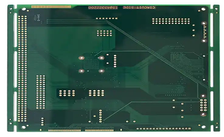
When it comes to high-performance electronics, 16-layer PCBs are a standout choice. These advanced printed circuit boards are designed for the most demanding applications, where performance, compact design, and precision are non-negotiable. But what exactly makes these boards unique? Let’s break down the core elements that set 16-layer PCBs apart from their lower-layer counterparts.
Multilayer PCB Technology Overview
First things first: What is a multilayer PCB? It’s a board made up of multiple layers of conductive materials, typically separated by insulating layers. The number of layers can range from just two (for a basic PCB) to upwards of 30 layers for the most complex designs. These layers are carefully arranged to provide routing for signals, power, and ground connections, all within a compact board.
16-layer PCBs are a type of multilayer PCB that offers a dense, highly functional design suited for high-end applications. By stacking 16 layers of copper and insulation, we can route more signals and provide efficient power distribution without requiring larger board sizes. The more layers, the more flexibility and complexity you have at your disposal.
Compared to simpler PCBs with fewer layers (like 4-layer or 8-layer boards), 16-layer PCBs are engineered to handle much higher frequencies, ensure better signal integrity, and optimize power distribution. If you’ve ever wondered why some advanced gadgets and devices look so small yet pack so much punch, it’s because of multilayer PCB technology—and the 16-layer designs are the crème de la crème.
| Feature | 4-Layer PCB | 8-Layer PCB | 16-Layer PCB |
| Signal Integrity | Good | Better | Excellent |
| Power Distribution | Moderate | Good | Optimized |
| Size Efficiency | Low | Moderate | High |
| High-Frequency Capability | Limited | Medium | High |
Core Advantages of 16 Layer PCBs
So, why choose a 16-layer PCB over other options? The advantages are clear and significant. Let’s break down the core benefits:
1.Enhanced Performance in High-Frequency and High-Speed Designs-
The primary reason for opting for a 16-layer PCB is its ability to handle high-frequency signals and high-speed data transmission. With more layers available for routing, 16-layer PCBs minimize the distance between signal paths, significantly improving signal quality and reducing delay. This is especially critical in industries like telecommunications and aerospace, where signal loss and crosstalk cannot be tolerated.
For example, when designing a high-frequency 5G mobile device, 16-layer PCBs enable us to route multiple signals in a compact space without compromising performance. The increased number of layers helps separate high-speed signal traces from noise, ensuring the integrity of each signal.
2.Better Impedance Control and Signal Routing-
In a 16-layer PCB, impedance control is much more finely tuned, which is especially crucial for high-speed digital circuits. The layers allow for better isolation of signals and more accurate control over the impedance between different traces. This results in fewer signal reflections, which can degrade the quality of high-speed signals in everything from data centers to medical imaging systems.
16-layer PCBs also offer better routing options. The increased number of layers provides more freedom for us to lay out components, improving routing efficiency and reducing the risk of signal interference. As multilayer PCBs allow us to make optimal use of limited space, these designs can handle more complex circuits with fewer compromises on performance.
Advanced Materials for 16 Layer PCBs
The materials used in the manufacturing of a 16-layer PCB are what allow these boards to perform so well under extreme conditions. Let’s dive into the materials that make these PCBs so special.
1.FR4 – The Workhorse of PCB Materials-
The FR4 substrate is one of the most commonly used materials in PCB production. It’s a fiberglass-reinforced epoxy resin that offers a good balance of mechanical strength, electrical properties, and cost-effectiveness. For most 16-layer PCBs, FR4 provides a reliable and durable base material. It is ideal for standard applications but can struggle when dealing with extreme temperatures or high-frequency operations.
2.Rogers – For High-Performance Applications-
For more demanding applications, such as military, aerospace, or high-speed communications, Rogers materials are the go-to. These high-performance substrates are known for their excellent thermal stability and superior electrical properties at high frequencies. Rogers materials also offer low dielectric loss and low signal attenuation, making them perfect for high-speed designs found in 16-layer PCBs used for advanced technologies like 5G, satellite communications, and high-frequency radar systems.
3.Material Considerations for Thermal Management and Durability-
Thermal management is another factor when designing 16-layer PCBs. As electronic devices become more powerful and compact, the need for efficient heat dissipation grows. Thermal vias and heat sinks are often integrated into multilayer PCB designs to help dissipate heat away from sensitive components. When designing 16-layer PCBs, the materials selected must not only handle high-frequency signals but also provide excellent thermal performance. High-quality materials, such as ceramic-based substrates or metal core PCBs, are used in more specialized designs to improve heat dissipation without compromising board strength.
Key Features of a 16 Layer PCB
When you’re looking at the best of the best in PCB technology, the 16-layer PCB stands out. It’s a sophisticated solution that excels in handling high-performance electronics, offering features that make it perfect for modern high-speed data transmission and space-constrained applications. Let’s break down the key features that define 16-layer PCBs and separate them from other designs.
High-Density Interconnection (HDI) Technology
One of the defining aspects of 16-layer PCBs is the incorporation of HDI technology. As electronic devices become smaller and more powerful, traditional PCB designs no longer meet the demands for performance and miniaturization. HDI technology is what enables 16-layer PCBs to maintain high performance while keeping the design compact.
Microvia and via-in-pad designs are the foundation of this technology. Microvias are small, precisely drilled holes that allow for signal transfer between the layers of the board. This not only makes the PCB more compact but also enhances signal transmission efficiency by reducing the path the signal travels. In 16-layer PCBs, these tiny vias enable a denser layout that doesn’t compromise on functionality or performance.
Via-in-pad designs optimize space by integrating vias directly into the component pads. This allows for more efficient routing, maximizing board space and making it perfect for applications like smart devices and medical equipment, where tight designs are needed. By stacking components and creating more room for additional circuits, this method ensures high-density designs without sacrificing performance. For industries where precision and compactness are must-haves, this approach helps get the most out of limited space, delivering top-tier functionality while keeping the design sleek and efficient.
| Design Feature | Traditional PCB | 16-Layer PCB |
| Signal Routing Density | Low | High |
| Via Size | Larger | Smaller |
| Space Utilization | Limited | Optimized |
| Design Complexity | Simple | High |
Signal Integrity and Power Distribution
Maintaining signal integrity and ensuring stable power delivery are two of the most pressing concerns in PCB design. For 16-layer PCBs, these factors are handled with precision, ensuring that the design can support high-speed, high-frequency applications without losing performance.
Signal integrity refers to the ability to transmit a signal without degradation or interference. 16-layer PCBs are designed with features that minimize issues like crosstalk and electromagnetic interference (EMI). By using ground planes and power planes between signal layers, we can effectively shield the signals from external noise and ensure high-quality data transmission.
In addition to signal integrity, power distribution is carefully managed in 16-layer PCBs. The design of power planes ensures that power is evenly distributed across the board, reducing voltage fluctuations and preventing noise from affecting sensitive components. This level of design precision makes 16-layer PCBs ideal for applications requiring high stability and minimal interference.
| Feature | 4-Layer PCB | 16-Layer PCB |
| Signal Integrity | Moderate | High |
| Power Distribution | Simple | Advanced |
| EMI and Crosstalk Mitigation | Basic shielding | Advanced isolation |
| Speed Capability | Low | High |
Thermal Management in 16 Layer PCBs
As devices get more complex, the heat they generate can really start to add up. Managing that heat effectively is a must for maintaining the longevity and performance of 16-layer PCBs. Overheating can lead to device failure, but with advanced thermal management strategies, 16-layer PCBs are built to handle high heat levels without compromising functionality.
One of the most effective ways to manage heat is through the use of thermal vias, which allow heat to transfer from the top layers of the PCB to the bottom, where it can be dissipated more effectively. In addition, the integration of copper planes within the PCB layers enhances the ability to conduct and spread heat across the surface, preventing hot spots that could affect the performance of sensitive components.
The design of the 16-layer PCB allows for the implementation of more advanced thermal techniques compared to simpler designs, ensuring that high-powered components continue to perform within safe thermal limits.
| Thermal Feature | 4-Layer PCB | 16-Layer PCB |
| Thermal Via Capability | Limited | Extensive |
| Copper Plane Integration | Basic | Advanced |
| Heat Dissipation Efficiency | Low | High |
| Temperature Control | Basic | Advanced |
How 16 Layer PCBs Are Manufactured?
Manufacturing a 16-layer PCB is no small feat. These complex circuits involve a multi-step process that combines advanced technology, high precision, and in-depth design optimization to create reliable, high-performance boards. Let’s walk through the entire process, from design to fabrication to testing, so you can get a clear picture of what goes into creating a state-of-the-art 16-layer PCB.
Design and Prototyping Process
Creating a 16-layer PCB begins with careful planning, where design software plays an integral role in ensuring everything lines up for a successful outcome. A well-executed design and prototyping process can save time, reduce errors, and improve overall performance.
●One of the first steps in the design process is layer stack-up optimization. This process ensures that the layers are arranged in such a way that the signals are routed as efficiently as possible. PCB design software allows our engineers to visualize the layer stack-up and fine-tune the placement of power planes, ground planes, and signal layers to maintain signal integrity and minimize electromagnetic interference (EMI).
●Furthermore, Simulation tools have completely transformed the design process. We can rely on signal integrity simulations to evaluate how well a PCB handles high-speed signals, ensuring that they travel smoothly without any loss. In addition, thermal simulations are used to assess how efficiently the board can dissipate heat across all 16 layers, preventing potential overheating issues. By using these tools early in the design phase, we can identify possible issues, adjust the design accordingly, and avoid costly mistakes later in the manufacturing process. It’s all about addressing problems before they escalate.
| Design Step | Without Simulation | With Simulation |
| Signal Integrity | Poor performance | Optimized routing |
| Thermal Management | Overheating risk | Balanced heat dissipation |
| Layer Stack-up Optimization | Manual adjustments | Precision adjustments |
Fabrication Techniques for 16 Layer PCBs
Once the design is finalized, it’s time to bring it to life using advanced fabrication techniques. The process of 16-layer PCB fabrication involves multiple steps, with particular attention to the sequential lamination process.
●In sequential lamination, the layers of the board are built up step by step. Each layer is laminated onto the previous one using a special adhesive that bonds the layers together. This technique allows for the creation of a multi-layer stack-up, with copper traces and vias connecting different layers. As 16-layer PCBs are complex, this step requires precision and a high degree of accuracy to ensure proper alignment of each layer.
●A key part of the fabrication process is via filling. Vias are small holes drilled through the PCB that provide electrical connections between layers. In a 16-layer PCB, these vias can be quite small, and they are filled with a conductive material to create the desired electrical connections between the layers.
●Laser drilling is a core technique in creating 16-layer PCBs, particularly when working with microvias. High-powered lasers are used to drill through the tiny layers with impressive accuracy. This precision enables the creation of microvias that facilitate high-density interconnects. By using lasers, the vias are drilled cleanly and accurately, reducing the chance of defects that could impact the overall performance of the PCB. In other words, laser drilling ensures that everything fits perfectly, allowing for more advanced and compact designs.
| Fabrication Step | Traditional Method | 16-Layer PCB Method |
| Layer Lamination | Standard press | Sequential lamination |
| Via Filling | Manual | Automated, precision filling |
| Drilling (Microvias) | Mechanical | Laser drilling |
Quality Assurance and Testing
After the fabrication process, it’s time to make sure everything works as expected. Quality assurance (QA) becomes a major focus at this point in the 16-layer PCB manufacturing process. Given the complexity of a design with so many layers and components, a detailed testing and inspection process is necessary to ensure the board functions reliably and performs at a high level. This includes checking the integrity of the layers, verifying the signal flow, and confirming that the vias and components operate correctly. Each step in QA is carefully executed to make sure the final product meets stringent standards and is ready for use in high-demand environments.
●One of the main methods used for QA testing is Automated Optical Inspection (AOI). This process uses cameras and sensors to visually inspect the PCB, looking for defects such as misaligned components or soldering errors. This technique ensures that the board meets the specifications and is free of any defects that could impact its functionality.
●Next, X-ray inspection is used for a more thorough analysis. For 16-layer PCBs, this step takes the spotlight because it uncovers issues that aren’t visible to the naked eye, like tiny voids in solder joints or flawed via connections buried within the layers. With so many intricately stacked layers, X-ray imaging becomes a powerful tool to ensure everything is lined up just right.
●Another testing method often used is flying probe testing. This technique uses a set of probes that touch various points on the board to check for electrical continuity. This is a faster and more efficient method than traditional bed-of-nails testing, allowing manufacturers to quickly verify that all electrical paths are functioning correctly before the PCB goes into final production.
●Finally, to ensure long-term reliability, stress testing is performed on the finished 16-layer PCBs. This involves subjecting the board to extreme conditions such as high temperatures, vibrations, or electrical loads to simulate real-world usage. Stress testing helps to identify any potential weaknesses in the design and manufacturing process, ensuring that the final product can withstand the demands of high-performance applications.
| Testing Method | Traditional PCB | 16-Layer PCB |
| Automated Optical Inspection | Visual check | High-speed optical checks |
| X-ray Inspection | Basic check | In-depth internal analysis |
| Flying Probe Testing | Limited coverage | Full electrical validation |
| Stress Testing | Optional | Rigorous, extended testing |
Cost and Customization Options for 16 Layer PCBs
Navigating the cost-performance tradeoff for 16-layer PCBs can feel like threading a needle. As these boards are designed to handle high-density interconnections and complex signal routing, they come with a unique set of manufacturing challenges and customization possibilities. Let’s take a look at the factors that influence the cost of 16-layer PCBs and explore the options available for tailoring these boards to meet specific needs.
Factors Affecting the Cost of 16 Layer PCBs
The price tag of a 16-layer PCB isn’t set in stone—it’s shaped by a mix of factors that all pull their weight. The choice of materials, the intricacy of the layout, and the production volume all play into the final cost. High-grade laminates and advanced copper weights, for instance, can push costs higher, while simpler designs and bulk orders might ease the strain on your wallet. Getting the lowdown on these elements can make a world of difference when it comes to keeping your budget in check without cutting corners.
1.Material Choice-
The choice of materials has a significant impact on the overall cost. FR4 is one of the most common substrates used in 16-layer PCBs due to its cost-effectiveness, but for high-performance applications, other materials such as Rogers, Teflon, or polyimide may be used. These materials offer superior thermal conductivity, signal integrity, and resistance to high-frequency noise, but they come with a premium price tag. For instance, Rogers materials are often used in high-frequency designs because they reduce signal loss, but they can raise costs by as much as 50% compared to standard FR4.
2.Design Complexity-
The more intricate your design, the higher the costs are likely to be. A 16-layer PCB involves multiple layers with complex routing and often requires high-density interconnects. The use of microvias, via-in-pads, and blind/buried vias all add to the complexity of the design, and the more complex the design, the more it will cost to manufacture.
3.Production Volume-
The number of units you plan to produce is another crucial cost factor. Prototyping small batches or low-volume runs often incurs higher per-unit costs due to setup fees and the manual inspection processes required. However, when producing large volumes, we can achieve economies of scale that help bring the cost per unit down.
| Cost Factor | Impact on Price | Example |
| Material | High-end materials increase cost | Rogers (high-performance) |
| Design Complexity | Complex designs increase cost | Use of microvias, HDI |
| Production Volume | Larger volumes reduce unit cost | 10,000 units vs 500 units |
Customization Possibilities for High-Performance Applications
Customization is often necessary to ensure that 16-layer PCBs meet the specific requirements of demanding applications such as those in aerospace, automotive, or telecommunications industries. Let’s look at some of the top options for tailoring your 16-layer PCB to meet your performance needs.
1.Rigid-Flex Designs-
Rigid-flex PCBs combine the best of both worlds: the stability of a rigid board and the flexibility of a flexible PCB. These designs are ideal for compact and space-constrained applications like wearables, medical devices, or drones. By integrating rigid-flex technology into a 16-layer PCB, you can create a board that is both reliable and adaptable to tight spaces, without sacrificing performance. This customization allows for more creative designs while maintaining the required electrical performance.
2.HDI Integration-
High-Density Interconnect technology involves utilizing microvias, fine-pitch components, and buried vias to create dense routing in a smaller area. By integrating HDI into 16-layer PCBs, we can achieve higher performance with a smaller footprint. This is especially useful for devices like smartphones, tablets, and other consumer electronics, where compactness is a must without sacrificing signal integrity or electrical efficiency. With HDI technology, we can pack more functionality into less space without losing performance quality.
3.Thermal Management Customization-
In high-performance systems, thermal management is a must. 16-layer PCBs can be customized to include copper planes, thermal vias, or heat sinks to better dissipate heat from high-power components. Thermal vias are drilled through the layers to provide a path for heat to travel from the top layers to the bottom, while copper planes act as heat sinks to absorb and distribute heat. Customizing the thermal layout ensures that your 16-layer PCB can handle the heat demands of advanced systems, reducing the risk of overheating or performance degradation.
| Customization Option | Impact on Performance | Applications |
| Rigid-Flex Design | Provides flexibility and space savings | Wearables, medical devices |
| HDI Integration | Enables high-speed, dense routing | Smartphones, tablets |
| Thermal Management | Prevents overheating | High-power systems |
Achieving Cost-Effective Solutions
Achieving the right balance between cost and performance is essential when designing 16-layer PCBs. Several strategies can help reduce costs without compromising the board’s performance.
1.Design Optimization-
By optimizing the design early on, you can minimize the need for expensive revisions or rework. This involves creating a layer stack-up that ensures efficient signal routing while minimizing the number of vias. Additionally, by utilizing design software that incorporates simulation tools for signal integrity and thermal analysis, you can identify potential problems before they become costly.
2.Material Selection-
If high-performance materials aren’t absolutely necessary, choosing more cost-effective options like standard FR4 can bring significant savings. In applications where signal integrity and heat management aren’t as critical, opting for less expensive materials can reduce costs without compromising functionality.
3.Prototyping and Testing-
Using rapid prototyping techniques and 3D printing for initial testing can save time and reduce costs during the design phase. This allows you to test various design options before committing to the full-scale production of your 16-layer PCB. Furthermore, performing automated testing (like flying probe testing) during the manufacturing process ensures that defects are caught early on, preventing costly fixes in later production stages.
| Cost-Reduction Strategy | Impact | Example |
| Design Optimization | Minimizes costly revisions | Early use of simulation tools |
| Material Selection | Reduces material costs | Using FR4 for less critical designs |
| Prototyping and Testing | Cuts testing and production costs | Rapid prototyping with 3D printing |
Signal and Power Integrity Challenges in 16 Layer PCBs
Designing 16-layer PCBs presents a number of challenges when it comes to maintaining signal integrity and ensuring reliable power distribution. These challenges become even more pronounced in high-speed designs, where small missteps can result in significant performance issues. Let’s take a closer look at the key challenges and the strategies for managing signal integrity, optimizing power distribution, and addressing the ever-present concern of electromagnetic interference (EMI).
Managing Signal Integrity in High-Speed Designs
In the world of high-speed PCB design, maintaining signal integrity is one of the biggest hurdles. With 16-layer PCBs handling more complex circuits, the risk of signal degradation becomes higher. To mitigate this, our engineers must employ precise routing techniques and methods to control impedance across the entire board.
1.Impedance Control-
Maintaining consistent impedance across the layers of a 16-layer PCB ensures that high-speed signals travel smoothly without interference or reflection. Signal integrity is directly influenced by the controlled impedance of the traces, especially as the speed of signals increases. Signals that are not routed properly can experience reflection and signal loss, leading to slower data transmission and degraded performance. This is why many designs employ microstrip or stripline structures, which allow for better impedance control.
2.Route Carefully-
In 16-layer PCBs, signal routing needs to be planned meticulously to prevent signal crosstalk or interference from neighboring layers. We often use tools like signal simulation software to model and analyze the layout before committing to production. Additionally, maintaining an appropriate trace width and spacing ensures that the signals remain within their impedance tolerance range. A high-quality PCB design tool can help automate much of the routing process and identify potential integrity issues before they occur.
3.Use of Ground and Power Planes-
Ground and power planes are used extensively in 16-layer PCBs to ensure that the signals are stable and the grounding system is noise-free. This minimizes the risk of interference and provides a solid reference for the signals traveling through the PCB.
| Signal Integrity Technique | Impact on Design | Example |
| Impedance Control | Reduces signal reflections and losses | Microstrip or stripline traces |
| Careful Routing | Minimizes crosstalk and interference | Use of high-speed routing tools |
| Ground and Power Planes | Provides stable reference for signals | Shielding and noise reduction |
Power Distribution Network (PDN) Optimization
A Power Distribution Network (PDN) in a 16-layer PCB is responsible for delivering consistent and stable power to all components across the various layers. As designs become more complex, ensuring that the power reaches every part of the board without drops or noise becomes more challenging. Let’s break down the aspects of PDN optimization for 16-layer PCBs.
1.Decoupling Capacitors-
Properly placing decoupling capacitors across the power distribution network helps to filter out high-frequency noise, ensuring that the components get a clean and steady supply of power. These capacitors smooth out voltage spikes and provide a local reserve of energy, which helps in reducing the impact of sudden voltage changes. In 16-layer PCBs, where power supply noise can easily cause problems, the exact placement and value selection of these capacitors can make all the difference.
2.Plane-to-Plane Coupling-
To ensure stable voltage and efficient current flow, the connection between the power plane and the ground plane must be carefully managed. We design the power planes to minimize any unwanted coupling between them, which helps reduce noise and prevent power loss. The layout of these planes directly affects how well power is delivered and how well signals maintain their integrity. By optimizing the stack-up configuration, we can make sure the power reaches its destination effectively, while also keeping signal quality in check.
3.Via-Types and Placement-
The type and placement of vias within the PDN are fundamental to ensuring that power is distributed evenly across the PCB. Via-in-pad and blind vias are commonly used to connect the different layers of the power distribution network. When placed correctly, these vias reduce voltage drop and resistance, ensuring power delivery with minimal loss. Proper via arrangement helps keep everything working as it should, optimizing the performance of your board and preventing unnecessary disruptions.
| PDN Optimization Technique | Impact on Power Delivery | Example |
| Decoupling Capacitors | Filters out noise and stabilizes voltage | Correct placement and value selection |
| Plane-to-Plane Coupling | Minimizes power loss and noise | Optimized stack-up design |
| Via-Types and Placement | Ensures efficient power distribution | Use of via-in-pad and blind vias |
Techniques to Mitigate Electromagnetic Interference (EMI)
Electromagnetic interference is a constant concern when dealing with 16-layer PCBs, especially as more components are crammed into smaller spaces. EMI can cause data loss, signal corruption, and even complete failure of the PCB if not properly managed. Fortunately, several shielding strategies and layer management techniques can help mitigate EMI.
1.Shielding Techniques-
The use of shielding layers is one of the most common methods for preventing EMI. In 16-layer PCBs, a dedicated ground plane or shielding layer can be placed between sensitive signal layers to block out external interference. This shielding acts as a barrier that absorbs or deflects electromagnetic waves, preventing them from reaching critical components.
2.Layer Stack-up Design-
The layer stack-up design directly impacts EMI reduction. By carefully arranging signal layers, ground layers, and power planes, our engineers can create electromagnetic shielding and ensure that noise is minimized across the board. For example, placing ground planes adjacent to signal layers can help shield them from interference.
JarnisTech offer the following standard 16-layer stack-up:
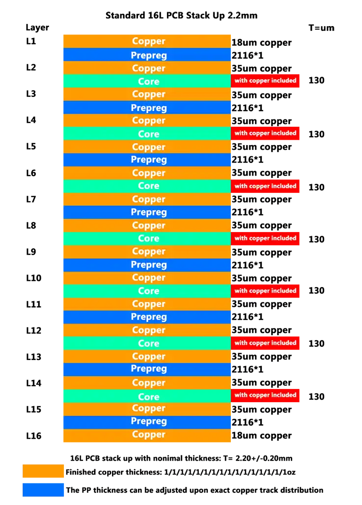
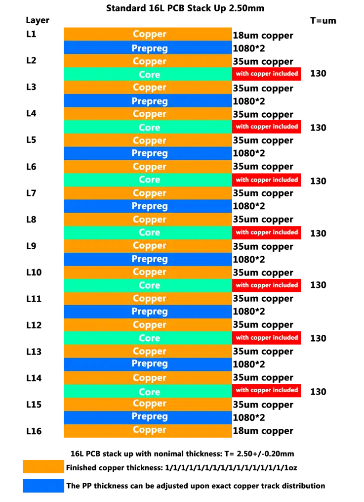
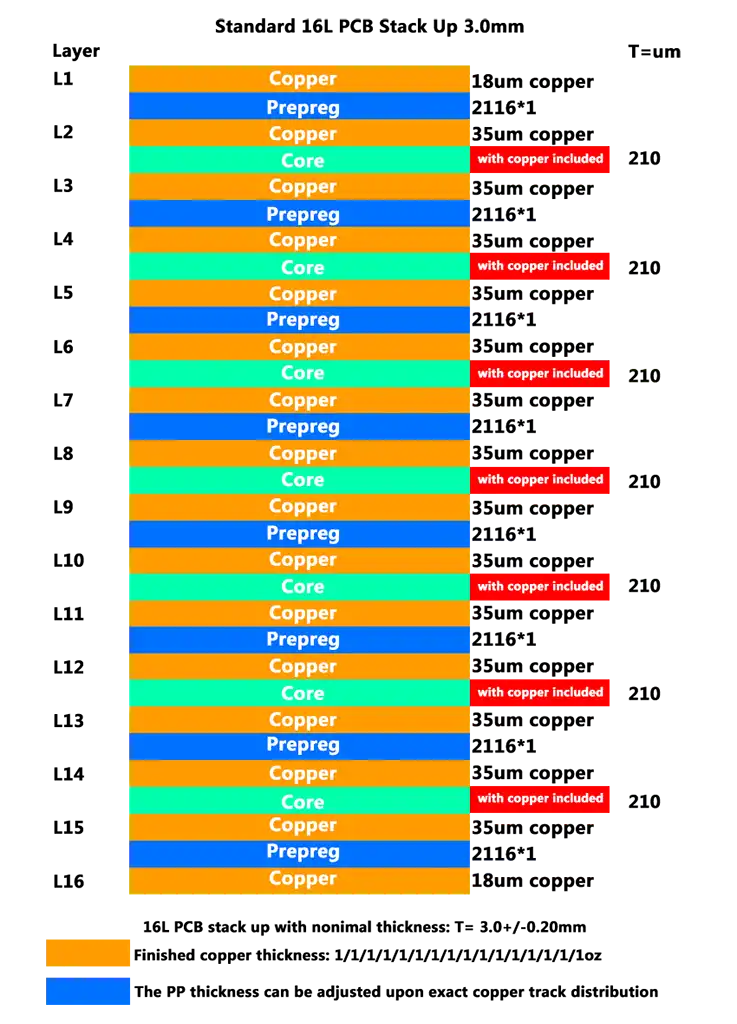
JarnisTech offers three standard 16-layer PCB options based on the best manufacturing features that balance quality and cost-effectiveness. We recommend utilizing Tg170 laminate materials for multilayer PCBs with over 6 layers to prevent any possible issues associated with PCB assembly procedures.
Our standard 16-layer PCB stack-up option consists of 1 oz finished copper thickness for each layer, ensuring optimal performance and reliability for multilayer rigid PCBs. This stack-up option is designed to meet the needs of a broad range of applications and manufacturing requirements.
If you need customized stack-up options for 16-layer circuit boards using impedance control or require a PCB stacking with 2oz or greater copper thickness, please don’t hesitate to reach out to us via email at [email protected]. Our team of experienced engineers can provide tailored solutions to meet your specific project requirements.
3.Minimizing Loop Areas-
One of the most effective ways to reduce EMI is by minimizing the loop areas in the power and signal traces. Large loops can act as antennas, radiating unwanted signals. By reducing the loop size, we can significantly lower the likelihood of radiated emissions and improve overall electromagnetic compatibility (EMC).
| EMI Mitigation Technique | Impact on Signal Integrity | Example |
| Shielding Layers | Blocks external interference | Ground shielding between layers |
| Layer Stack-up Design | Reduces EMI by proper arrangement of layers | Signal, ground, and power layers |
| Minimizing Loop Areas | Prevents radiated emissions | Tight routing and trace placement |
Innovations in 16 Layer PCB Technology
The world of 16-layer PCBs is continuously evolving, thanks to innovations in materials, fabrication techniques, and design strategies. As consumer electronics, aerospace applications, wearables, and IoT devices continue to demand faster, smaller, and more efficient solutions, the advancements in multilayer PCB technology push the boundaries of what’s possible. Here’s an exploration of some of the groundbreaking advancements that are shaping the future of 16-layer PCBs.
HDI and Microvia Advancements
High-Density Interconnect technology has revolutionized the way we design 16-layer PCBs, allowing us to create more compact, efficient boards that pack in more functionality. One of the key innovations in this field is the use of microvias—tiny, high-precision holes that allow for more layers in less space. Here’s how HDI and microvia advancements are pushing the limits of compact PCB designs:
1.Microvia Technology-
Microvias are small, laser-drilled holes that help connect traces across multiple layers of a PCB. These small holes enable the design of denser, more compact circuits, allowing for more efficient use of space in 16-layer boards. Microvias are particularly beneficial in high-speed designs where space is limited but performance cannot be compromised. Laser drilling ensures precision in creating microvias, reducing the risk of errors that could affect signal integrity.
2.Laser Drilling-
Laser drilling technology takes microvia creation to the next level, offering unmatched precision compared to older mechanical approaches. This method allows for the fabrication of multi-layer PCBs with intricate designs tailored for high-speed and high-frequency use. The smaller and cleaner vias produced by laser drilling make it possible to achieve tighter trace spacing and compact configurations, which are particularly suited for cutting-edge HDI designs. With this technology, 16-layer PCBs can handle complex layouts and demanding performance requirements without breaking a sweat.
3.Higher Layer Count and Density-
By utilizing HDI and microvias, we can increase the layer count without increasing the size of the board. This results in higher density designs that support the complex demands of modern electronics, from smartphones to automotive systems.
| Innovation | Benefit | Application |
| Microvia Technology | Increased density and compact designs | Wearables, IoT devices |
| Laser Drilling | Precise, high-performance vias | High-speed, high-frequency circuits |
| HDI Integration | Higher layer count with smaller boards | Smartphones, automotive electronics |
Integration of Rigid-Flex Technology
As devices get smaller and more complex, the need for flexible solutions becomes even more pronounced. Enter rigid-flex technology—a hybrid solution that combines the best of both worlds. Here’s how the integration of rigid-flex technology is reshaping the way we think about 16-layer PCBs:
1.Applications in Aerospace-
In the aerospace industry, where space is at a premium, rigid-flex technology allows for the creation of compact, lightweight PCBs that can be bent or folded to fit into tight spaces. The flexibility of these boards makes them ideal for satellite systems, aviation electronics, and other applications where weight and space are critical. For example, flexible parts of the PCB can be routed along curves in spacecraft, while rigid parts provide strong support for components that require stability.
2.Wearables and IoT Devices-
Rigid-flex PCBs are a perfect fit for the wearable technology and Internet of Things (IoT) markets. These applications require high-density connections, durability, and flexibility to conform to the shape of the device. Smartwatches, fitness trackers, and other wearables utilize rigid-flex designs to offer compactness, durability, and reduced form factor while still delivering high performance.
3.Design Versatility-
One of the standout features of rigid-flex PCBs is their ability to combine rigid PCB layers with flexible circuitry, giving us the flexibility to create intricate, three-dimensional designs without compromising reliability. This versatility has made rigid-flex PCBs a go-to solution for industries ranging from medical devices to automotive systems, where flexibility and performance are a must.
| Rigid-Flex Application | Benefit | Industry Use |
| Aerospace | Space and weight-saving designs | Satellite systems, avionics |
| Wearables | Conforms to compact, flexible shapes | Smartwatches, fitness trackers |
| Automotive | Increased durability and efficiency | In-vehicle electronics |
Why Choose Us for Fabrication of 16 Layer PCBs?
At JarnisTech, we specialize in delivering high-quality, custom 16-layer PCBs that meet the most stringent industry standards. With a proven track record and a wealth of expertise, we’re your go-to partner for all your PCB needs. Here’s why we stand out:
Our PCB Manufacturing Capabilities:
1.Unmatched Versatility in PCB Types: We pride ourselves on offering a diverse range of PCBs tailored for various industries, from consumer electronics to aerospace and telecommunications. Whether you need multilayer PCBs or HDI PCBs, our manufacturing capacity is vast. Our 16-layer PCBs are particularly sought after for their superior performance and ability to handle high-speed, high-density applications.
2.Rigid and Flexible PCBs: We can create rigid PCBs with up to 60 layers, perfect for complex applications that demand high-layer counts and intricate design features. If you’re looking for a more dynamic solution, we offer rigid-flex technology, which can handle up to 20 layers, providing a robust yet flexible solution for devices that require both stability and adaptability.
3.Metal-based PCBs for Specialized Applications: We offer metal-based PCBs, including copper and aluminum options, tailored for high-power setups where managing heat is non-negotiable. These boards are designed to handle demanding applications, with support for up to 8 stacked layers. Whether it’s power electronics, LED lighting systems, or automotive technology, these PCBs bring the heat—literally—by efficiently dissipating thermal energy. Their rugged design and multi-layer capabilities make them a go-to solution when reliability and performance need to go hand in hand.
4.Extensive Range of Substrate Materials: When it comes to substrate materials, we understand that one size does not fit all. We offer a wide range of substrates, including:
●FR4: Ideal for most standard applications
●High-frequency FR4: Designed for applications requiring higher signal integrity
●Ceramic: Perfect for high-temperature, high-power scenarios
●Halogen-free FR4: Environmentally friendly, meeting global green standards
●Polyimide and PTFE hybrid: Best for flexible, high-frequency applications
These substrates are precisely selected to match the unique demands of your project, ensuring optimal performance in every aspect.
5.Surface Finishing Options:A good surface finish is non-negotiable when it comes to PCB reliability and longevity. We offer a broad selection of surface finishes, including:
●Immersion Silver & Tin: Great for excellent conductivity and solderability
●HAL Lead-free: For eco-friendly, lead-free options
●ENIG (Electroless Nickel Immersion Gold): Offers a strong, corrosion-resistant finish
●OSP (Organic Solderability Preservative): Cost-effective and environmentally friendly
●Hard Gold Plating: Best for precision applications
●Blue Mask & Carbon Ink: For aesthetic and functional enhancements
HDI PCB Fabrication Expertise:
We excel at fabricating HDI PCBs with intricate layer stack-ups, such as 1+n+1 and 7+n+7 stacked vias, ensuring your design is executed with precision. Our engineers are well-versed in advanced HDI technologies, and our state-of-the-art equipment guarantees tight tolerances and superior quality. No matter the complexity of your design, we can create HDI PCBs that deliver superior signal integrity and high-performance characteristics.
Advanced PCB Technologies for Customized Solutions:
At JarnisTech, we don’t just fabricate standard PCBs—we offer a range of specialized technologies to meet the unique needs of our clients. These include:
●Conductive and Non-Conductive Via Filling: For higher reliability and improved signal integrity in high-density boards.
●Back Drilling: To eliminate signal loss in multi-layer designs.
●Edge Plating: Ideal for providing additional durability to the edges of your PCB, protecting against mechanical stress.
●Heavy Copper PCBs (up to 20 oz): These are perfect for high-power applications where heat dissipation is crucial.
●Vias-in-Pad Filling: A solution for making your PCB design more compact while maintaining reliable electrical connections.
We’re also equipped to handle high-frequency microwave and RF circuit boards, allowing us to create highly precise and reliable PCBs for industries like telecommunications and defense.
Commitment to Quality and Precision:
With our dedicated team of PCB engineers, your project is in safe hands. From design to prototyping and mass production, we offer tailored solutions that meet your exact requirements. We place a strong emphasis on delivering top-tier quality, ensuring that each 16-layer PCB is manufactured to meet global industry standards. Our commitment to precision, cost-effectiveness, and efficiency allows us to deliver superior products with fast turnaround times.
FAQs related to 16-layer PCBs
Why would I choose a 16-layer PCB for my design?
A 16-layer PCB is ideal for high-speed, high-frequency applications that require superior performance, such as telecommunications, automotive, and medical devices.
What are the challenges when designing a 16-layer PCB?
The main challenges include managing signal integrity, controlling impedance, and ensuring proper layer stacking and via placement.
How do I control signal interference on a 16-layer PCB?
Proper layer stack-up, including placing ground planes close to signal layers and using power planes effectively, can minimize signal interference.
What materials are used in 16-layer PCBs?
Common materials include FR4 for general purposes, while high-frequency applications may use materials like Rogers or PTFE for better performance.
PCB Fabrication
Multilayer PCB Manufacturing & Assembly


