
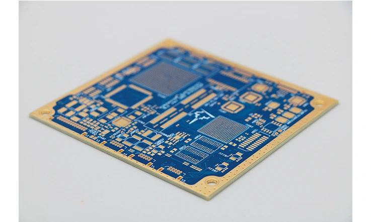
High-speed PCB designs are all the rage in today’s electronics world, focusing on printed circuit boards that are optimized for transmitting and receiving signals at jaw-dropping frequencies. These PCBs are the backbone of countless devices, including computers, smartphones, routers, and high-speed data communication systems. Operating at signal frequencies that can reach several gigahertz, the significance of mastering high-speed design principles, routing strategies, and layout considerations can’t be overstated, especially when tackling challenges like electromagnetic interference (EMI).
With the rise of groundbreaking technologies such as 5G, the Internet of Things (IoT), and artificial intelligence (AI), designers are under pressure to create PCBs that can handle rapid communication, processing, and data storage. Just think of it as being on the front lines of innovation—if you want to keep up, you’ve got to play your cards right!
To achieve stellar high-speed design results, adhering to the foundational principles of high-speed design is a must. Are you ready to explore these principles and elevate your PCB designs to new heights?
Let’s dive right in and unlock the secrets to high-speed success!
Principle 1: Grounding Techniques
Effective Ground Plane Design for Signal Integrity
When it comes to PCB design, grounding often takes a backseat, but it’s a game-changer for ensuring signal integrity. A robust ground plane serves as the go-to reference for all signals, helping to keep electromagnetic interference (EMI) at bay.
Common Pitfalls: One frequent oversight is skimping on ground plane area. If the ground plane is too small, it can lead to higher impedance and unwanted noise. To steer clear of this, aim for a ground plane that covers as much area as possible without unnecessary cuts or breaks.
Pro Tip: Use a solid ground plane along with multiple vias. This setup creates a low-impedance path for return currents, helping to keep your signals clean and crisp.
Benefits of Proper Grounding in High-Speed Applications
Nailing your grounding strategy can lead to a noticeable uptick in overall circuit performance. When done right, proper grounding reduces noise and minimizes the chance of signal loss, resulting in a design you can trust.
Technical Insight: A continuous ground plane can significantly cut down on ground bounce, maintaining signal integrity by providing a stable reference voltage. Think of it like a solid foundation for your house—it keeps everything from wobbling and falling apart.
Example of Effective Grounding
Consider a high-speed digital circuit where grounding issues led to frequent signal integrity problems. By redesigning the ground plane to be larger and using multiple vias, the team saw a dramatic reduction in noise and a smoother signal. This change not only improved performance but also saved time during testing.
Key Benefits Table
| Benefit | Impact on Design |
| Reduced Noise | Cleaner signal transmission |
| Enhanced Signal Integrity | Fewer errors and improved reliability |
| Lower Ground Bounce | More stable performance under high-speed conditions |
Reflective Questions
How does your current grounding strategy stack up against these principles? Are there opportunities to amp it up?
Don’t wait! Take a moment to assess your grounding techniques and see where you can make improvements. It might just be the boost your design needs!
Principle 2: Routing Strategies for PCB Layout
Best Practices for Layer Stack-Up Configuration
Layer stack-up is the secret sauce of PCB design—get it right, and everything runs like a well-oiled machine. A carefully planned stack-up configuration can effectively manage high-speed signals, cutting down on crosstalk and ensuring a smooth signal path.
Example: Take a high-speed circuit where power and ground layers are placed adjacent to signal layers. This strategic layout can boost performance by minimizing inductance and helping signals flow without a hitch.
Optimizing Via Placement for Improved Performance
When it comes to via placement, thinking ahead is essential. Misplaced vias can introduce unwanted inductance, throwing a wrench in your signal quality.
Technical Insight: Aim to use blind and buried vias whenever possible. These types of vias shorten the length of signal paths, helping maintain the integrity of high-speed signals. Think of it like taking a shortcut to avoid traffic!
Utilizing Differential Pairs for Enhanced Signal Clarity
Differential pairs are a real game-changer in high-speed designs. By routing these pairs closely together, you can effectively cancel out unwanted noise, leading to a more reliable signal.
Industry Application: This technique is commonly used in USB and HDMI designs, where high-speed data transfer is a must. The payoff? Clearer signals and fewer headaches during troubleshooting.
Example of Effective Routing
Imagine a design team working on a new USB interface. Initially, they struggled with crosstalk and signal degradation. By rearranging the layer stack-up and implementing differential pairs, they saw a marked improvement. The signals became sharper, and the design passed testing with flying colors!
Key Benefits Table
| Benefit | Impact on Design |
| Reduced Crosstalk | Clearer signal paths |
| Enhanced Signal Integrity | Fewer errors and improved reliability |
| Shortened Signal Paths | Quicker response times |
Reflective Questions
What strategies are you currently using to manage routing on your boards? Are there ways you can kick it up a notch?
Don’t just sit there! Take a moment to review your routing techniques and see where you can make improvements. Your designs will thank you!
Principle 3: Impedance Control in High-Speed Design
Significance of Impedance Matching and Control
Impedance matching is a cornerstone of high-speed design. When there’s a mismatch, reflections can pop up, leading to data loss that no one wants to deal with.
Tools for Measurement: Leverage tools like Time Domain Reflectometry (TDR) to measure and adjust impedance levels in real time. This helps ensure that your signals hit the sweet spot every time.
Techniques to Maintain Consistent Impedance for Signal Integrity
Keeping impedance consistent is all about the details. Techniques such as controlled trace width and spacing play a vital role in achieving this.
Example: For RF applications, using a 50-ohm trace width is standard practice. This not only helps maintain optimal signal transmission but also keeps your design running smoothly.
Example of Effective Impedance Control
Take a look at a design team developing a high-speed communication interface. They noticed reflections causing data integrity issues. By carefully measuring impedance with TDR and adjusting trace widths accordingly, they managed to eliminate reflections. The result? A cleaner signal and a design that passed all tests without a hitch!
Key Benefits Table
| Benefit | Impact on Design |
| Reduced Reflections | Enhanced data transmission |
| Consistent Signal Integrity | Fewer errors during operation |
| Improved Overall Performance | More reliable high-speed communication |
Reflective Questions
How do you currently validate impedance in your designs? Are there steps you can take to elevate your game?
Now’s the time! Dive into your impedance validation process and see where you can step things up. Your designs will reap the rewards!
Principle 4: Managing EMI and EMC Issues
Key Strategies for EMI Reduction in High-Speed PCBs
EMI can really throw a wrench in the works for high-speed designs, but with the right strategies, you can keep it at bay.
Best Practices: Implementing solid grounding techniques, careful routing, and incorporating ferrite beads can make a world of difference in reducing EMI. These steps are like having a safety net for your signals.
Shielding and Filtering Approaches for EMC Compliance
Ensuring electromagnetic compatibility (EMC) is a must-have for any high-speed design.
Data Insight: A study revealed that effective shielding can cut EMI by as much as 30%, which can significantly boost your design’s reliability. Think of shielding as wrapping your circuit in a protective bubble.
Example of Effective EMI Management
Consider a design team developing a new wireless communication device. Initially, they faced significant EMI issues, leading to data dropouts. By applying a combination of grounding techniques and shielding, they managed to reduce EMI drastically. Their device not only passed EMC testing but also performed reliably in real-world conditions.
Key Benefits Table
| Benefit | Impact on Design |
| Reduced EMI | Improved signal integrity |
| Enhanced EMC Compliance | Greater design reliability |
| Lower Risk of Interference | More stable performance in challenging environments |
Reflective Questions
What measures are you currently taking to minimize EMI in your designs? Are there ways you can kick it up a notch?
Don’t wait! Take proactive steps today to reduce EMI in your designs. Your circuits will thank you for it!
Principle 5: Power Distribution Network (PDN) Design
Ensuring Power Integrity Across the PCB
A well-designed power distribution network is essential for keeping voltage levels steady across the board. Think of it as the lifeblood of your PCB—if the power isn’t stable, nothing else will work right.
Technical Insight: Strategically placing decoupling capacitors near power pins is a smart move. This helps maintain voltage levels during transient events, ensuring your components get the juice they need exactly when they need it.
Strategies for Efficient Power Distribution in High-Speed Applications
Utilizing techniques like decoupling capacitors and thoughtful trace design can significantly enhance power distribution.
Example: Imagine a PDN design that prevents voltage sag during peak loads. When a high-speed processor ramps up, a well-planned PDN ensures that all components operate optimally, keeping your system running smoothly.
Example of Effective PDN Design
Take a design team working on a high-performance computing system. They faced issues with voltage drops during heavy workloads. By implementing a robust PDN with carefully positioned decoupling capacitors, they were able to eliminate voltage sag and enhance overall performance. The end result? A system that runs like a champ under pressure!
Key Benefits Table
| Benefit | Impact on Design |
| Stable Voltage Levels | Reliable component performance |
| Reduced Voltage Sag | Optimal operation during peak loads |
| Enhanced Overall System Performance | Improved efficiency and longevity |
Reflective Questions
How effective is your current power distribution strategy in preventing voltage drops? What changes can you make today to improve it?
Don’t just sit there! Take a good look at your PDN design and see where you can tighten things up. Your circuit will thank you later!
Principle 6: Thermal Management Techniques in PCB Design
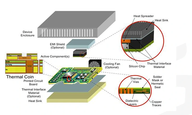
Understanding Heat Dissipation Needs in High-Speed Designs
Heat can be a silent killer in electronic designs. As components operate, they generate heat that, if not managed properly, can lead to failures that will make you pull your hair out.
Best Practices: Consider implementing thermal vias and heatsinks to effectively dissipate heat. These techniques act like a safety valve, allowing excess heat to escape and keeping your components cool.
Design Strategies for Effective Thermal Management
Engineers should integrate thermal analysis during the design phase to identify potential hotspots before they become a problem. It’s like looking under the hood before taking your car for a spin.
Data Insight: Thermal simulations can predict temperature rise, helping you design effective thermal management solutions. By visualizing heat flow, you can make informed decisions about where to place heatsinks and thermal vias.
Example of Successful Thermal Management
Imagine a design team developing a high-performance graphics card. Initially, they noticed overheating issues during intense gaming sessions. By conducting thermal simulations, they identified hotspots and added thermal vias and a larger heatsink. The outcome? A cooler, more reliable card that gamers love.
Key Benefits Table
| Benefit | Impact on Design |
| Effective Heat Dissipation | Enhanced reliability of components |
| Proactive Hotspot Identification | Avoidance of thermal-related failures |
| Improved Overall Performance | Increased efficiency in high-speed applications |
Reflective Questions
What thermal management strategies have you found effective in your designs? How can you ensure optimal performance moving forward?
Don’t let heat be the silent killer in your designs! Take a hard look at your thermal management approach and see where you can make improvements. Your components will thank you for it!
Principle 7: Testing and Validation Protocols for High Speed PCB
Importance of Rigorous Testing for High-Speed Designs
Testing isn’t just a checkbox on your to-do list; it’s a critical part of the design process that can make or break your project. Think of it as the final inspection before a big race—no one wants to hit the track with a faulty vehicle!
Validation Techniques: Techniques like In-Circuit Testing (ICT) ensure that each component functions as intended. This method provides real-time feedback and helps catch issues early, saving you time and headaches later on.
Common Validation Methods for Ensuring Signal Integrity
Utilizing techniques such as Time Domain Reflectometry (TDR) and eye diagram analysis is essential for validating your high-speed designs. These methods act like a magnifying glass, allowing you to see potential problems before they become costly errors.
Data Insight: Eye diagrams can reveal how much jitter and noise are present in your signals, helping to fine-tune your design for optimal performance. It’s like tuning a guitar—just a little adjustment can make all the difference.
Example of Effective Testing Protocols
Consider a team developing a high-speed communication module. Initially, their prototypes exhibited inconsistent performance. By implementing rigorous testing protocols, including TDR and eye diagram analysis, they were able to identify and correct signal integrity issues. The end result? A module that consistently outperformed expectations and delighted their customers.
Key Benefits Table
| Benefit | Impact on Design |
| Enhanced Signal Integrity | More reliable and robust designs |
| Early Problem Detection | Saves time and resources |
| Increased Customer Satisfaction | Higher confidence in product performance |
Reflective Questions
How rigorous is your testing process for ensuring signal integrity? What steps can you take to kick it up a notch?
Now’s the time! Evaluate your testing procedures and make improvements to boost your design’s reliability. Your future self will thank you!
Collaborating with a Trusted High-Speed PCBs Manufacturer

When diving into the fundamentals of high-speed printed circuit board (PCB) design, engaging in conversations with a reputable PCB manufacturer and assembler is a smart move. With so many options out there, it’s essential to team up with a certified and seasoned company that knows the ropes.
Why Choose JarnisTech?
JarnisTech stands out in the high-speed PCB manufacturing and assembly arena. Our commitment to the key principles of high-speed PCB production ensures that your projects don’t just meet the mark—they exceed expectations. We take pride in our ability to customize solutions tailored to fit your specific business needs, giving you that edge in a competitive market.
Example of Our Expertise:
For instance, if you’re working on a project that demands low EMI and high signal integrity, our team can help design a PCB that includes advanced grounding techniques and optimized routing strategies. This way, you can rest assured that your final product will perform like a charm.
| Feature | JarnisTech Advantage |
| Customization | Tailored solutions to meet unique needs |
| Expertise | Over 20 years in high-speed PCB design |
| Quality Assurance | Rigorous testing protocols for reliability |
| Support | Knowledgeable team ready to assist |
Get in Touch
If you want to learn more about how JarnisTech can help bring your high-speed PCB projects to life, don’t hesitate to reach out to our friendly team today. We’re here to help you every step of the way, ensuring your designs not only look good on paper but also work seamlessly in the real world.
Final Thoughts
High-speed PCB design is a challenging yet rewarding field that requires attention to detail and a solid understanding of essential principles. By adhering to these guidelines, engineers can navigate the complexities of high-speed designs, delivering reliable and high-performance PCBs.
Ready to elevate your PCB design skills? Start implementing these principles today!
Frequently Asked Questions (FAQ)
What are the typical challenges in high-speed PCB design?
Engineers often face challenges such as managing EMI, ensuring signal integrity, and maintaining thermal efficiency.
How can signal integrity be enhanced in my designs?
Utilizing differential pairs, proper routing strategies, and impedance matching are effective ways to enhance signal integrity.
Why is thermal management critical in high-speed applications?
Proper thermal management prevents overheating, which can lead to component failure and degraded performance.


