
The utilization of 8-layer PCB stackups has experienced significant growth in various industries and applications. The versatility and expanding use cases of 8-layer PCBs make it a crucial component in modern electronic systems.
This article aims to provide a comprehensive understanding of 8-layer PCBs. We will delve into their definition, outline important design guidelines, and highlight key factors to consider when selecting an experienced PCB designer.
Why Should You Use A Standard 8 Layer PCB Stackup
In typical PCB designs, the choice often falls on single or double-layer PCBs, as they typically meet the project requirements adequately. Simplicity in PCB design is crucial to minimize the potential risks associated with unnecessary complications. However, certain situations demand the adoption of a multilayer PCB design. Although less common, an 8-layer PCB stackup is employed in specific applications.
A multilayer PCB generally refers to a printed circuit board comprising three or more conductive layers. These conductive layers are positioned between prepregs and an insulative core in the PCB stackup. Prepregs represent raw insulated materials, commonly FR4, while the core incorporates copper layers.
As electronic devices continue to shrink in size and signal speeds increase, multilayer PCBs become a viable solution. In a standard PCB layer stackup, a minimum of four copper layers are dedicated to signal traces. This configuration allows for increased space on the outer layers to accommodate components effectively.
Moreover, PCB designers rely on multilayer PCBs to enhance signal integrity within their designs. Signal layers within a standard 8-layer PCB stackup are isolated by power and ground planes. These internal planes play a crucial role in minimizing crosstalk between signal layers, thereby bolstering signal integrity.
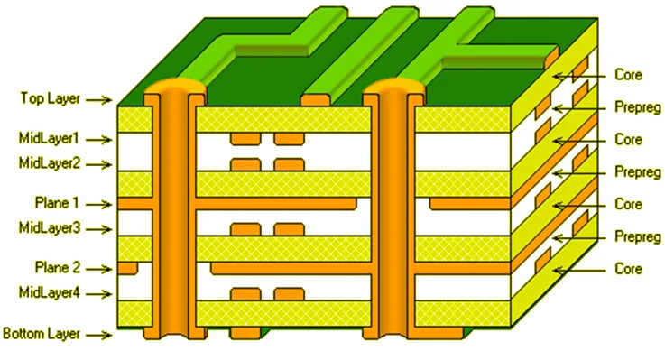
What is an 8 Layer PCB Stackup?
An 8-layer printed circuit board (PCB) represents a sophisticated multilayer design comprising four signal layers and four planes that are intricately stacked. The layer configuration includes dedicated ground and power planes, which act as barriers between the signal layers. These planes serve the purpose of minimizing undesirable crosstalk between signals and provide inter-plane capacitance, thereby enhancing signal integrity. The strategic arrangement of layers in an 8-layer PCB contributes to improved performance.
The utilization of an 8-layer PCB stackup offers ample space for efficient routing of numerous power islands. This enables the reduction in size of complex components while simultaneously enhancing operational speed. The construction of an 8-layer PCB involves the implementation of more than the standard four layers of conductive materials. This additional layering serves to optimize the performance of signal traces, resulting in increased overall efficiency.
The integration of an 8-layer PCB involves the establishment of robust and interconnected connections among all layers. This meticulous layer stacking ensures reliable signal propagation throughout the PCB. Moreover, the incorporation of extra planes in the 8-layer PCB stackup significantly enhances its electromagnetic compatibility (EMC) performance. Furthermore, the additional layers in this stackup provide enhanced routing capabilities, facilitating the efficient layout of complex circuitry.
Materials Used in an 8-layer PCB Stack-up
In the construction of 8-layer printed circuit boards (PCBs), a stack of alternating conductive and dielectric layers is utilized. Several commonly employed conductive materials in this PCB assembly include:
●Copper: Copper is the most prevalent material found in 8-layer PCBs due to its cost-effectiveness and excellent conductivity. Additionally, copper is readily recyclable, providing an environmentally friendly option for users.
● Gold: Although not as widely used as copper, gold is still a viable choice for conductive material in 8-layer PCBs due to its exceptional conductivity. However, it should be noted that gold comes at a higher cost compared to copper.
● Aluminum: While not as popular as copper or gold, aluminum serves as a suitable material for carrying high-current traces in 8-layer PCBs. These traces are typically thick and require a material capable of handling heat and current without incurring excessive costs.
Regarding the substrate materials used in 8-layer PCBs, the following options are commonly employed:
● Polyimide: Polyimide is a favored dielectric material in 8-layer PCBs due to its low dielectric constant and loss tangent. It is particularly well-suited for high-frequency applications and environments with elevated temperatures.
● FR-408: FR-408 is another widely used dielectric material for 8-layer PCBs, offering a lower dielectric constant and loss tangent compared to polyimide. It proves to be a suitable choice for high-speed digital applications.
● Arlon AD2000: Arlon AD2000 is a dielectric material characterized by its very low dielectric constant and loss tangent. It is frequently employed as a standard choice in 8-layer PCBs.
●Rogers RO400: Rogers RO400, known for its exceptionally low dielectric constant and loss tangent, is a popular choice for 8-layer PCBs. It is particularly well-suited for high-frequency and high-speed applications.
These conductive and dielectric materials play crucial roles in ensuring the electrical performance and reliability of 8-layer PCBs, making them essential considerations during the PCB manufacturing process.
Best Practices for 8-Layer PCB Stackup Design
While an 8-layer stackup can be beneficial for mitigating EMI concerns, it is crucial to understand that it is not a cure-all solution. To maximize the advantages of a multilayer stackup, it is essential to adhere to best practices in PCB layout design. Here are some key considerations:
1. Routing Direction: In an 8-layer PCB stackup with 6 signal layers, it is advisable to route signal traces on adjacent layers perpendicularly to minimize cross talk. It is prudent to establish the habit of routing signal layers differently on subsequent layers, even when separated by power or ground planes.
2. Return Path: It is vital to visualize the return path of high-speed signals, even if they are on the inner layers. Ensuring a short and interference-free return path for signals is crucial to maintain signal integrity and prevent interference with other components.
3. Ground Plane: It is generally recommended to avoid having a split ground plane as it can create impedance discontinuity. Additionally, for components on the outer layer, it is important to establish low-impedance connections to the inner ground planes through vias.
4. Buried or Blind Vias: To further optimize routing space, the use of buried or blind vias can be considered. However, it is advisable to consult with the manufacturer to confirm their capability to produce such vias in the PCB.
Designing an 8-layer PCB can be made easier with the assistance of appropriate software tools. For example, the Cross Section Editor in OrCAD PCB Designer offers comprehensive control over the layer stackup. Whether you require robust Design Rule Check (DRC) tools, efficient documentation management and production processing, or reliable analysis and simulation capabilities, you can trust JarnisTech to provide the necessary solutions for your design requirements.
If you are seeking further information or assistance, our team If you’re looking to learn more about how JarnisTech has the solution for you, please feel free to reach out to us and our team of experts. We are here to help you with your 8-layer PCB design needs.
Advantages of 8-Layer Stack-ups
The utilization of 8-layer stack-ups in PCB designs offers several advantages that can greatly enhance the performance and functionality of electronic circuits. Here are some key advantages of employing 8-layer stack-ups:
Increased Routing Space:
An 8-layer stack-up provides ample routing space for complex and densely packed circuits. With four signal layers, there is more room to route traces, connect components, and accommodate high-density designs without compromising signal integrity.
Enhanced Signal Integrity:
The separation of signal layers by dedicated power and ground planes helps minimize crosstalk and electromagnetic interference (EMI). The presence of internal planes provides shielding and reduces noise, resulting in improved signal integrity and reduced signal degradation.
Improved Power Distribution:
The inclusion of power and ground planes in an 8-layer stack-up enables efficient power distribution throughout the PCB. These planes act as low-impedance paths, reducing voltage drops and maintaining stable power supply to critical components.
Better Thermal Management:
With additional layers, it becomes feasible to dedicate specific layers to thermal management. Heat dissipation can be optimized by incorporating thermal vias and copper pours in these layers, ensuring efficient cooling of high-power components.
Design Flexibility:
The extra layers in an 8-layer stack-up provide greater design flexibility. Designers have more options for component placement, layer allocation, and routing strategies, enabling efficient and compact designs while meeting specific design requirements.
Enhanced Electromagnetic Compatibility (EMC):
The presence of multiple layers and dedicated ground planes helps improve EMC performance by reducing emissions and susceptibility to external interference. This is particularly important in sensitive applications where electromagnetic compatibility is a critical consideration.
Reduced Crosstalk:
The additional internal layers in an 8-layer stack-up act as effective barriers between signal layers, minimizing the potential for crosstalk. This results in cleaner signal transmission, reduced signal distortion, and improved overall circuit performance.
Higher Density and Miniaturization:
The use of an 8-layer stack-up allows for higher circuit density and miniaturization. The additional layers provide more space for routing and component placement, enabling the integration of complex functionalities into smaller form factors.
Comparing 8-Layer vs. 6-Layer PCB Stackups
When evaluating the options for PCB stackup configurations, one can consider the 6-layer and 8-layer alternatives. These stackups differ not only in their layer count but also in terms of performance characteristics.
As the name implies, the 6-layer PCB stackup comprises fewer layers compared to the 8-layer counterpart. Consequently, the 8-layer PCB stackup entails additional layers, resulting in higher overall costs.
It should be noted that the 8-layer PCB stackup offers enhanced performance compared to the 6-layer configuration. This improvement can be attributed to several factors. Firstly, the increased layer count provides a larger area for component placement, facilitating better component density and more efficient routing. As a result, signal impedance can be effectively reduced, leading to improved signal integrity.
Furthermore, the additional layers in the 8-layer PCB stackup contribute to mitigating issues related to electromagnetic interference (EMI). By strategically allocating dedicated ground and power planes, the stackup design helps to minimize EMI problems, ensuring better overall system reliability and performance.
Comparing 4-Layer and 8-Layer PCB Stackups
When considering different PCB stackup configurations, two common options are the 4-layer and 8-layer stackups. These alternatives possess distinct characteristics in terms of layer count, cost, and performance.
Starting with the 4-layer PCB stackup, it comprises a relatively lower number of layers compared to the 8-layer configuration. As a consequence, the 4-layer stackup generally involves simpler and more cost-effective manufacturing processes. The reduced layer count also translates to lower material costs, making it a more budget-friendly option.
However, it’s important to note that the 4-layer stackup has certain limitations in terms of performance. With fewer layers available for routing and component placement, the design space can be more constrained. This may result in challenges such as increased signal impedance and limited room for addressing electromagnetic interference.
On the other hand, the 8-layer PCB stackup offers distinct advantages over its 4-layer counterpart. By doubling the layer count, the 8-layer stackup provides additional layers for routing, allowing for improved signal integrity and reduced signal impedance. The extra layers also offer more flexibility in component placement, enabling higher component density and more efficient designs.
Additionally, the increased layer count in the 8-layer stackup allows for dedicated power and ground planes, aiding in the management of power distribution and minimizing potential EMI issues. This can significantly enhance the overall reliability and performance of the PCB.
Nevertheless, it’s important to consider that the 8-layer stackup is associated with higher manufacturing costs compared to the 4-layer option. The additional layers, materials, and manufacturing complexity contribute to the increased expenses.
Cost Factors in 8-Layer PCB Stackup Design
Designing an 8-layer PCB incurs costs, and it is important to have a rough estimate to avoid budgetary surprises. Several factors contribute to the increase in the cost of designing an 8-layer PCB stackup:
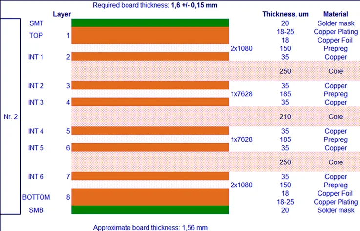
1. Number of Layers: An 8-layer PCB actually consists of four layers and four planes. The complexity and number of layers impact the overall cost of design and manufacturing.
2. Size of the Board: The size of the board, determined by the number and size of components, affects the cost. Packing more components into a smaller space increases the complexity and cost of the design.
3. Size of Holes: The number and size of holes on the PCB influence the costs. More holes or the use of super-thin holes require additional work during production, leading to increased costs.
4. Type of Finish: The type of finish used on the PCB can impact costs, although it is considered a minimal factor. Different finish options offer various advantages, such as improved solderability or extended shelf life. Common finishes for 8-layer PCBs include ENEPIG, HASL, IMM Ag, OSP, Elec Au, LFHASL, ENIG, and IMM Sn.
Considering these factors and their impact on costs can help you plan your budget effectively when designing an 8-layer PCB stackup.
How to Find the Best 8 Layer PCB Stackup Manufacturer?
Selecting a reliable and competent 8-layer PCB manufacturer requires patience and careful consideration to ensure that the desired design outcomes are met. Here are some essential factors to consider when seeking the services of an 8-layer PCB manufacturer:
1. Personalized Service: It is advantageous to engage with a PCB manufacturer that provides dedicated one-to-one service, allowing for consistent support throughout the 8-layer PCB stackup process. This ensures real-time collaboration and cost-effective design facilitation. Furthermore, a manufacturer offering comprehensive services can assist in material sourcing, ensuring efficient design, manufacturing, and timely dispatch.
2. Professionalism: It is crucial to partner with an 8-layer PCB manufacturer that possesses relevant experience and expertise. Assessing their professional background, including certifications and industry recognition, is essential in making an informed decision about their capabilities.
3. Order Capacity: Consider whether the chosen manufacturer has the capacity to handle your project requirements, both in terms of quantity and timeline. Verify if they can accommodate the minimum quantity you intend to design and manufacture, and assess their ability to meet project deadlines without compromising quality.
4. Turnaround Time: Evaluate whether the 8-layer PCB manufacturer can facilitate the design and manufacturing process within a reasonable timeframe. If a quick turnaround is essential, discuss the feasibility of meeting your desired delivery time. It is important to ensure that the manufacturer can deliver the completed design in excellent condition when you need it.
By carefully evaluating these factors and engaging with a reputable 8-layer PCB manufacturer, you can enhance the likelihood of obtaining the desired design outcomes without any unexpected surprises.
Conclusion
An effectively designed 8-layer stack-up plays a critical role in achieving optimal electrical performance, signal integrity, power distribution, and electromagnetic compatibility in PCB designs. The utilization of an 8-layer stack-up offers several advantages, including enhanced design flexibility, improved signal integrity, efficient power distribution, and suitability for high-density designs.
However, it is important for designers to carefully consider factors such as complexity, cost, signal integrity limitations, and routing feasibility when selecting an 8-layer stack-up for their PCB design. Achieving precise impedance control and maintaining signal integrity in 8-layer stack-ups requires meticulous planning, accurate calculations, and adhering to established design guidelines. By taking these factors into consideration and implementing appropriate techniques, designers can ensure the reliable and efficient operation of their electronic circuits.


