The printing circuit boards (PCB) fabrication process is an intricate procedure to ensure the performance of the PCB product. Although circuit boards can be single-sided, double-sided or multilayer, only after the first layer is produced do the fabrication processes differ. Because of the different designs of PCBs certain PCBs may require more stages during the manufacturing process.
The amount of steps needed to create printed circuit boards corresponds with their level of complexity. Cutting any step out or reducing the process can negatively affect how the board performs. When the procedure is successfully completed the PCBs must be able to complete their functions properly as vital electronic components.
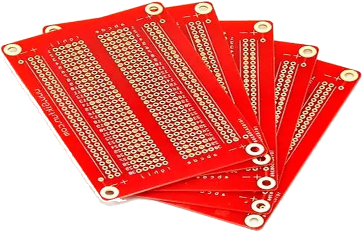
PCB Manufacturing Step by Step Guide:18 Steps
The majority of printed circuit boards are constructed from copper. Copper is typically plated to a substrate and carved away to reveal the board design. Because there are multiple layers, they must be aligned and bonded together to make the board a perfect fit.
Design: Step 1
Before you start making the PCB, you must be able to have a design of the board. The blueprints are what you will base your manufacturing procedure on. This design phase is typically accomplished using computer software. Utilizing a measure of the width of a trace will assist with the majority of information needed for the inner and outer layers.
The Printing Of The Designs: Step 2
A specific printer, also known as the plotted printer is employed to print the design on the PCB. It prints an image that displays the various layers that make up the circuit board. If printed it will have two colors of ink that are used on the interior layers of the board. Clear Ink shows the non-conductive areas, and Black Ink shows the copper conductors and circuits.
Similar colors will be used in the outer layer, however, their meaning is reversed.
Making the Substrate:Step 3
The PCB is now beginning to form. Substrate consists of insulating materials (epoxy resin and glass fiber) that hold components on a structure together. Substrate is formed through oven semicuring. Copper is prebonded to both sides of the layer, which is then etched away to reveal the design.
Printing The Inner Layers:Step 4
It is printed on a laminate, and the main body of the structure is then constructed. A photo-sensitive film composed of photo-reactive chemicals which will become hard when exposed to UV sunlight (the resist) will cover the design. This will aid in aligning the blueprints with the actual print on the board. Holes are made in the PCB to facilitate aligning.
Ultraviolet Light:Step 5
After aligning, the resist and laminate are exposed to ultraviolet light to harden the photoresist. The light reveals the paths of copper. The black ink used prior stops the formation of hardened areas to be removed later. It is cleaned in an alkaline solution, which helps get rid of all excess photoresist.
Eliminating Copper That Is Not Needed:Step 6
Now is the time to eliminate any undesirable copper that has remained in the boards. Chemical solutions like an alkaline solution consume the copper that was not wanted. The hardened photoresist is left intact.
Inspect:Step 7
The freshly cleaned layers will have to be checked to determine alignment. The holes made earlier can assist in aligning the outer and inner layers. An optical punch machine will drill holes with a pin to ensure that the layers are aligned. Following the laser punch is completed, another machine will examine the board to confirm that there aren’t any defects. If you have missed any errors, they cannot be fixed from this point on.
Laminate the Layers: Step 8
Then, you can be able to see the board taking form when the layers are fused together.As the laminating process begins, metal clamps hold the layers together. The preparing (epoxy resin) layer is laid over the basin for alignment. A layer of substrate is applied over the prepreg, followed by the copper foil and then more prepreg resin. Finally, there is another copper layer to form known as the press plate.
Pressing the Layers: Step 9
Mechanical presses are employed to force the layers to each other. For some technologies, pins are punched through layers to ensure alignment and security. Depending on the technology, you may be able to remove these pins. Once the pins are aligned correctly, the PCB will be put through a laminating press, which applies heat and pressure to the layers. By melting the epoxy within the prepreg and applying pressure, the layers are bonded together.
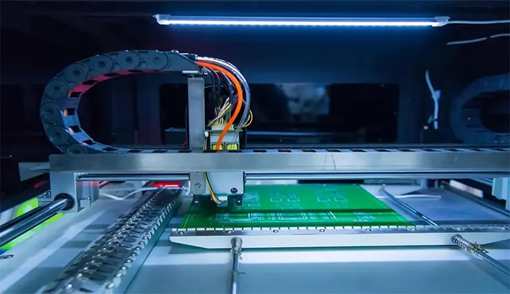
Drilling: Step 10
Holes are cut into the layers using the use of a computer-guided drill, which exposes the panels and substrate. The remaining copper after this process is removed.
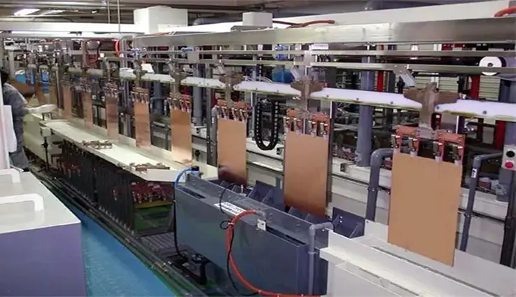
The Plating: Step 11
The board is ready to be Plating. A chemical solution is used to bond all the layers. The board is then cleaned using a different set of chemicals. These chemicals also cover the board with a thin copper layer, which can penetrate into the holes.
Outer Layer Imaging: Step 12
Then, a layer of photoresist, will be applied on the outside layer prior to being sent to imaging. Ultraviolet light sets the photoresist. The unwanted photoresist is eliminated.
Plating: Step 13
the panel is coated with a thin copper layer. Following this, the thin tin shield is applied on top of the panel. Tin is used to safeguard the copper of the outer layer from being removed.
Etching: Step 14
Remove any unwanted copper under the resist layer using the same chemical solution as before. The tin guard layer shields the copper that is required. This is the process that made the PCB’s connections.
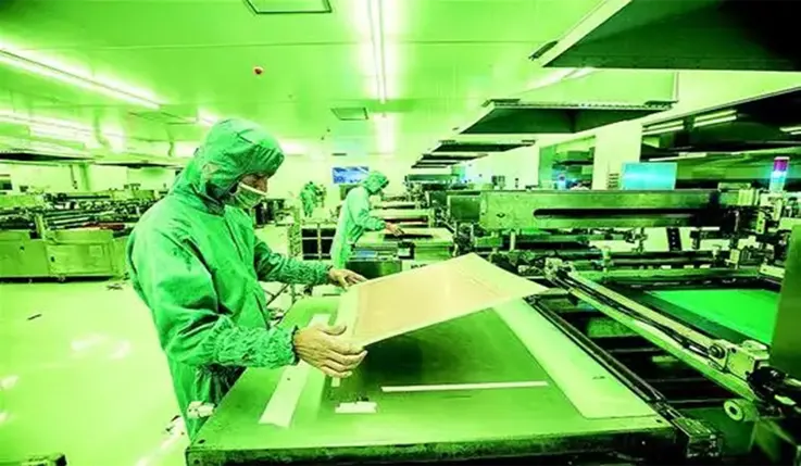
Solder Mask Application:Step 15
Before applying the solder mask, all panels should be cleaned. The epoxy is applied using the soder mask film. The solder mask is applied to the green color that you normally observe on a PCB. Any unneeded solder mask is removed using ultraviolet light. The desired mask is baked onto the board.
Silkscreening:Step 16
Silkscreening is an important procedure since it is the one that prints crucial information on the board. Once applied,the PCB goes through a final coat and cure process.
Surface Finish:Step 17
The PCB is coated in either a solderable surface or a non-sealable one according to the needs that will improve the bond strength and quality that the solder has.
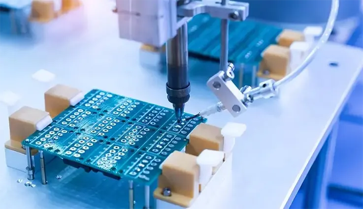
Test:Step 18
Prior to the PCB being deemed complete, A technician will conduct an electric test of the PCB. This test will verify that the PCB functions and conforms to the original blueprint design.
PCB Fabrication Process: Is it Important
The question asks: “Is it important to be aware of the PCB fabrication procedure?” After all, PCB fabrication isn’t an activity for design but is an outsourced task that is handled with the help of a contractor producer (CM). However, while it’s true that the manufacturing isn’t a design job but it is performed strictly in accordance with the specifications you give for your CM.
Most of the time the case, your CM isn’t aware of the design intention or performance goals. So, they won’t know if you’re making the right selections for the layout, materials locations, types via locations and trace parameters, or any other aspects of your PCB that you will be determined during the process of fabrication and can influence your PCB’s manufacturability production yield rate, or performance following deployment as outlined below:
Fabricability
The Fabricability of your boards is based on a variety of designs you choose to make. This includes ensuring that sufficient clearances are present between the elements of the surface and the edge of the board and that the chosen material has a high CTE (CTE) to withstand PCBA in particular for non-lead soldering.Both of these may result in your board not being able to be built without reworking. Furthermore, You will also need to think ahead if you decide to panelize your designs.
Yield Reduction
Your board can be constructed successfully, but there are issues with fabrication. For example, setting parameters that go beyond the tolerance limits of the equipment used by your CM could cause in higher than acceptable numbers of boards that are unusable.
High Reliability
Based upon the purpose of your circuit board’s purpose, it’s classified in accordance with the IPC-6011. For PCBs that are rigid, there are three levels of classification that specify the parameters your board’s design must satisfy to attain a certain degree of reliability. If your board is constructed to be a lower class than the one your application demands will cause inconsistent operation or premature failure of the board.
So, the solution is definitely yes! It is essential to be aware of how to go about the PCB fabrication process since the decisions you make at this stage will echo throughout PCB manufacturing, development, and even into operation. The best way to protect yourself from the kind of problems that result from not taking into account knowledge regarding PCB manufacturing process in your design choices is to use the design for manufacture (DFM) regulations and rules dependent on the abilities of the CM.
How To Implement An Effective PCB manufacturing Process
The design and fabrication processes involved in PCB manufacturing are often performed by different entities. In many instances contractors (CM) can produce PCBs using the same design that was developed by the OEM (OEM). Collaboration on design, components as well as file formats and materials for boards between these two groups will guarantee a smooth process and smooth transition between the phases.
Components
Before PCB manufacturing and assembly, the designer should consult the fabricator about available components in advance. The ideal is that the fabricator would have all the necessary components for the design in stock If something is missing, the designer and the fabricator must find the best solution to speed up production, while also meeting the minimum specifications for the design.
Design For Manufacturing (DFM) Things To Consider
During the design process, it is important to consider whether the design is capable of progressing through the various stages of fabrication. Often, the manufacturer(CM) has an established list of DFM guidelines for their facility which the OEM can refer to when designing the product. The designer may request this DFM guideline to guide their PCB design in order to adjust to the fabrication process of the fabricator.
File Formats
Communication between OEM as well as CM is essential for ensuring the full fabrication of the PCB according to the specifications of the OEM’s design. Both groups should use the same formats to design PCB. By doing this, you can avoid mistakes or loss of information that might be caused by files that have to be formatted.
Board Materials
OEMs can create printed circuit boards using more expensive materials than what the CM expects.It is crucial for both parties to agree on what materials are available and what will work best for the PCB design without sacrificing cost-effectiveness.
The Final Words
The above are all the solutions to “how can a PCB be made step-by-step”. In actual fact, during the manufacturing process of professional PCBs, because of the diverse requirements of the clients for various circuit board materials as well as the different requirements for PCB manufacturing, There will be some slight gaps in the PCB board manufacturing process. Jarnis Technologies will continue to keep up-to-date on this issue on this blog. Of course, if anyone has specific knowledge about the manufacturing processes of PCB, You can send us anytime.