Printed circuit boards (PCBs) are critical components of modern electronic devices, providing a platform for connecting various electronic components and enabling their precise control. The development of a new PCB design requires careful planning, design, and manufacturing, all of which entail significant costs.
PCB non-recurring engineering (NRE) refers to the one-time expenses associated with the development of a new PCB design, including design layout and prototyping, tooling preparation, and other non-recurring costs. These costs are primarily incurred in the early stages of the product development cycle and can have a significant impact on the overall project budget and timeline.
Careful management of PCB NRE is critical to ensuring the overall profitability of the final product. In this article, we will discuss the key factors that affect PCB NRE, strategies for reducing these costs, and best practices for successful management of PCB NRE throughout the product development cycle. By understanding the key considerations involved in PCB NRE, you can make informed decisions that will help ensure the success of your product development efforts while minimizing the associated costs.
What Is Non-Recurring Engineering (NRE) ?
As an electronic manufacturer, NRE, or Non-Recurring Engineering, is a term that refers to the comprehensive investment needed to successfully take a new product project from ideation to large-scale production. This investment covers all costs associated with the development of the new launch, from its conceptual stage to mass production, and it represents a one-time expense.
NRE costs involve all expenses incurred during the pre-production phase, including investments in critical requirements like molding tools, die casting tooling, fixtures and jigs, and test rigs that are necessary to uphold consistent product quality during mass production. It is widely recognized that this stage is pivotal for new launches as the decisions made during pre-production determine the impact of the product on the market.
Understanding NRE costs is crucial for electronic manufacturers when developing a new product. Proper planning, early identification of requirements, and efficient utilization of resources during this phase can help to minimize overall costs while maximizing the success of the product launch.
PCB Non-recurring Engineering
PCB non-recurring engineering (NRE) refers to the one-time costs associated with the development of a new printed circuit board design, ranging from initial concept to final product release. These costs typically include activities such as design layout, prototyping, and tooling preparation, as well as any other non-recurring expenses that may arise during the manufacturing process. The NRE cost is a significant factor in any PCB design project, and it should be carefully managed to ensure the product’s overall profitability.
What Is the PCB NRE Cost ?
As a PCB manufacturer, NRE (Non-Recurring Engineering) is an essential charge that incorporates the development, design, and testing of new PCB designs, in addition to up-front costs incurred during the design and manufacturing of a new product. This charge is an inevitable part of any PCB manufacturing process.
It is crucial to budget and plan for NRE costs as part of the project plan. This charge includes the cost of labor, materials for prototypes, and testing products, as well as expenses incurred during pre-production requirements and activities, encompassing all software and electronics development.
It’s important to note that NRE is a one-time cost. Hence, every process and material should undergo thorough review and analysis to ensure that the NRE cost accurately reflects the production or unit cost of the product.
To ensure that NRE expenses are correctly allocated, PCB manufacturers must prioritize proper planning, early identification of requirements, and efficient use of resources during the design and development phase. This approach will help to minimize overall costs and maximize the chances of a successful product launch.
PCB NRE Cost Estimation and Factors Affect
PCB NRE cost estimation is a critical aspect of the PCB NRE process. The following are some of the factors that can affect the cost of a PCB NRE project:
● Complexity of the design: The more complex the PCB design, the more time and resources required to develop it, which can increase the NRE cost.
● Prototype iterations: If multiple iterations are required for a PCB design, this can increase the overall NRE cost.
● Materials: The type of materials used for the PCB can affect the NRE cost. For example, specialty materials or high-grade copper can be more expensive.
● Labor costs: The cost of the labor required to design and manufacture the PCB can be a significant factor in the NRE cost estimation.
● Testing requirements: The more rigorous the testing requirements for a PCB design, the more expensive the NRE cost can be.
● Tooling costs: Tooling costs, such as the cost of making a steel stencil for the PCBs, can also be a factor in NRE cost estimation.
Accurate NRE cost estimation is important to ensure that a PCB NRE project is completed within budget and on time.
What Are the Common PCB Non-recurring Engineering Costs ?
As a PCB design engineer, it’s important to have a comprehensive understanding of NRE (Non-Recurring Engineering) charges and tooling costs in the PCB industry. NRE costs in PCB manufacturing are divided into two categories, covering non-recurring engineering tooling costs and programming expenses. It’s worth noting that these costs are not based on the main regular cost of the NRE.
Non-recurring engineering tooling cost is unique to each customer and is added to the regular NRE cost for that particular customer. This cost covers tools that are crucial for specific customer orders, including metals, press-fits, artworks, stencils, jigs, and other important tools.
The tools used in NRE tooling are highly selective, and the expenses required for them are non-recurring. They are mainly used to design products as per customer requirements. After completing the design process, the customers receive their orders.
● Programming: In PCB manufacturing, a setup fee, also known as “programming costs,” is necessary when programming machines for producing a specific PCB. This fee covers the labor and time required to program the machines, and it is a non-recurring cost. Once the programming is completed, the contract manufacturer can use the programmed data to produce the PCBA.
To accurately calculate the NRE cost in PCB manufacturing, programming costs play a crucial role. It’s worth noting that these costs vary based on the complexity and particular needs of the PCB designs. As such, careful planning, efficient utilization of resources, and early identification of programming requirements can help to minimize the overall cost and ensure successful product launches.
● Tooling: In the PCB manufacturing process, specific tools are collected, and their costs are added up to form the NRE (Non-Recurring Engineering) cost. These tools include fixtures, metals, stencils, artwork, among others, and are made specifically for a particular product and customer. For example, solder stencils are unique and can only be used for one type of circuit board, making them like fingerprints.
Once a stencil is designed and fabricated for a specific PCB, there’s no need to make new stencils to continue manufacturing the assembly. However, the tooling cost is often the most complicated item when it comes to circuit board production as it constitutes a significant portion of the overall NRE cost.
It is essential to note that consistency is a vital factor when calculating tooling costs. Some engineers make the mistake of assuming that the PCBs involved in a project require multiple layers, leading to an overestimation of the tooling cost.
Therefore, as a PCB design engineer, careful planning, meticulous identification of project requirements, and effective utilization of resources is imperative in managing the tooling cost.
Strategies for Minimizing PCB NRE
Minimizing non-recurring engineering (NRE) costs associated with printed circuit board (PCB) manufacturing is a crucial aspect of any successful PCB design project. Implementing effective strategies for reducing NRE costs can help ensure that a project stays within budget and meets its timeline goals. Here are some strategies for minimizing PCB NRE costs:
● Choose a PCB fabrication company that offers comprehensive design support and has a thorough understanding of the nuances of PCB design and fabrication. This way, the fabrication company can work collaboratively with the design team to identify and address any potential design or manufacturability issues early in the development process, helping to minimize the need for design iterations.
● Optimize your design for manufacturability. This involves designing your PCB layout in a way that simplifies the manufacturing process, minimizes the use of specialized tools and materials, and reduces the number of necessary fabrication steps. By designing a board layout that is simpler and easier to manufacture, you can minimize the costs associated with tooling preparation and production runs.
● Use simulation and testing tools to identify any potential design or manufacturing issues early in the product development cycle. This approach helps avoid expensive design iterations later in the process, reducing NRE costs.
● Consider using off-the-shelf or pre-validated components in your PCB design rather than creating custom components from scratch. This can help reduce the design complexity and number of unique parts, ultimately simplifying the manufacturing process.
● Engage in value engineering activities that focus on optimizing the balance between design function, performance, and cost. This can help identify areas where cost savings can be achieved without sacrificing quality.
By implementing these strategies, you can reduce PCB NRE costs and help ensure that the design project stays within budget and timeline goals. Working collaboratively with both the design and manufacturing teams can further streamline the process and help minimize the risk of costly design iterations and fabrication errors.
Why Choose JarnisTech ?
● In the Printed Circuit Board (PCB) industry, the Non-Recurring Engineering (NRE) cost is an important factor that affects the success or failure of a product launch. The NRE cost comprises the NRE tooling and programming costs, which are necessary to provide a design in the orders. JarnisTech PCB stands out from normal PCBs by offering a greater number of tools to customers. Additionally, JarnisTech PCB provides two ways to pay the NRE cost: breakout and amortization.
● The breakout payment method requires customers to pay the entire NRE cost before paying the unit cost. This cost includes the NRE tooling cost and programming cost. In contrast, the amortized payment method allows customers to add the NRE cost, including the NRE tooling cost and programming cost, to the unit cost without having to pay the NRE cost upfront. While the breakout payment method is preferred by most customers due to its simplicity, the amortized method can be a viable option for some.
● Investing in the NRE process is crucial for the development of a successful product launch. The quality of machinery and tools used during the pre-production stages significantly impacts the final product’s performance and marketability. Hiring skilled employees, devising sound strategies, and utilizing advanced tools are crucial factors that contribute to the product’s success. Therefore, investing in high-quality products and prerequisites is essential for generating sales and profitability. Neglecting the NRE process can lead to significant losses in the long run.
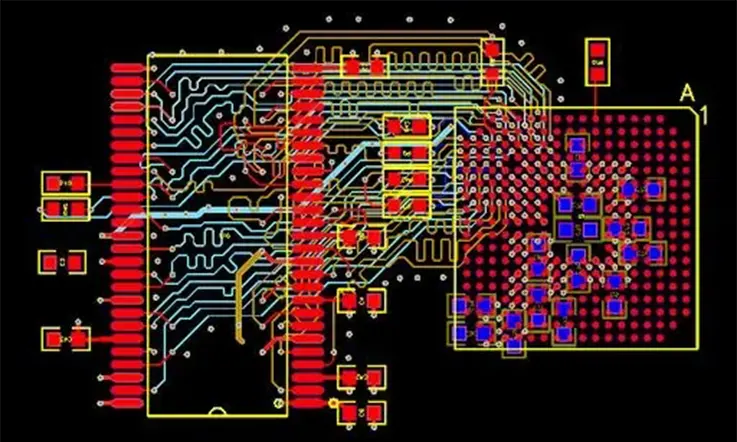
PCB NRE Design Considerations
PCB NRE design considerations play a crucial role in the success of a PCB project. The following are some of the important considerations related to PCB NRE design:

● PCB layout: The layout of the PCB plays a critical role in its functionality and performance. Designers must consider factors such as signal integrity, power integrity, and thermal management when designing the layout.
● Components: The selection of appropriate components for the PCB is essential to ensure optimal performance and reliability. Factors such as compatibility, availability, and cost must be considered when selecting the components.
● Materials: The type of materials used for the PCB can impact its performance, reliability, and manufacturability. Designers must consider factors such as thermal properties, dielectric constant, and thermal expansion when selecting materials for the PCB.
● Signal Integrity: Signal integrity is critical in ensuring that the PCB functions as intended. Designers must consider factors such as impedance, routing, and crosstalk when designing the PCB.
● Power integrity: Power integrity is essential to ensure stable power delivery to components on the PCB. Designers must consider factors such as decoupling capacitance, voltage drop, and current carrying capacity when designing power networks on the PCB.
● Thermal management: Effective thermal management is crucial to ensure the reliability of the PCB. Designers must consider factors such as heat dissipation, thermal conductivity, and thermal resistance when designing the PCB layout and selecting materials.
By taking into account these design considerations, designers can create a PCB that meets the performance specifications while also being reliable and manufacturable.
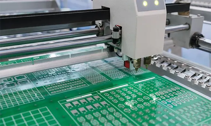
PCB NRE Manufacturing Process
The PCB NRE manufacturing process involves a series of steps, each of which requires specific equipment and expertise. The following are the key steps involved in PCB NRE manufacturing process and the equipment used:
● PCB design: The initial step in PCB NRE manufacturing is the design of the PCB. This step involves the use of specialized software such as Altium, Eagle or KiCAD to create the PCB layout.
● CAM processing: Once the design is complete, the data is converted into a format for manufacturing. This step is called CAM processing, which involves the use of software to generate the necessary manufacturing instructions.
● Pre-production: The next step is the preparation of materials and equipment before manufacturing can begin. This includes the selection of the appropriate materials, the calibration of the equipment, and the setup of the production line.
● Printing: The printing process involves the transfer of the PCB layout onto a laminate substrate using a photosensitive process. Equipment such as a plotter or printer is used to print the layout onto the laminate substrate.
● Etching: The next step is etching, which involves the removal of unwanted copper from the PCB using a chemical process. This process can be done either by hand or using specialized equipment called etching machines.
● Drilling: Once the copper has been etched away, holes must be drilled in the substrate for the insertion of components. This step involves the use of a drilling machine, which can create precise and accurate holes.
● Plating: The plating process involves the deposition of a thin layer of copper over the entire surface of the PCB. This layer serves to protect the circuitry and also helps to improve the conductivity of the PCB.
● Solder Mask: The next step is the application of a solder mask over the PCB. This step involves the use of specialized equipment such as a screen printer or spray gun to apply the solder resist.
● Component Assembly: The final step is the component assembly, which involves the placement of components on the PCB and their subsequent soldering. This step can be done manually or using automated equipment such as pick-and-place machines or SMT (Surface Mount Technology) machines.
By using appropriate equipment, materials, and techniques, manufacturers can ensure that the PCB is produced to the required specifications.
PCB NRE Quality Control and Testing Methods
Quality control and testing are crucial aspects of the PCB NRE process to ensure that the PCB is manufactured to the required specifications and meets the desired performance and reliability standards. The following are some of the quality control and testing methods used in PCB NRE:
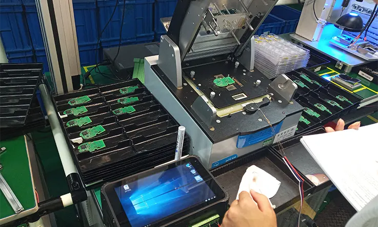
● Visual inspection: Visual inspection is the simplest and most common method used for quality control. It involves the visual inspection of the PCB for defects such as missing components, misaligned components, or soldering defects.
● Electrical testing: Electrical testing is a crucial aspect of PCB NRE. It involves the testing of the electrical properties of the PCB, such as impedance, continuity, and insulation resistance. Electrical testing equipment such as digital multimeters or oscilloscopes may be used to perform these tests.
● Functional testing: Functional testing involves testing the functional aspects of the PCB to ensure that it meets the performance requirements. This testing can be performed manually or using automated equipment and may involve simulating real-world scenarios to test the PCB’s performance.
● Thermal testing: Thermal testing involves subjecting the PCB to temperature extremes to ensure that it can operate reliably in high or low-temperature environments. This testing can be performed using environmental chambers or thermal shock testing equipment.
● X-ray Inspection: X-ray inspection is performed to check internal component and pad connections for accuracy and quality. The equipment used in this process includes x-ray machines.
● In-circuit testing: In-circuit testing involves testing the PCB’s components while powered on to identify defective or faulty components. It includes machine testing as well.
By applying a combination of these testing methods, manufacturers can ensure that the PCB is reliable, functional, and meets the required quality standards.
Case Studies of Successful PCB NRE Management
Effective management of non-recurring engineering (NRE) costs associated with PCB manufacturing is critical to ensuring the profitability and success of any PCB design project. Here are some case studies of successful PCB NRE management:
● CASE STUDY 1: A medical device manufacturer was developing a new PCB design for a specialized diagnostic tool. To minimize NRE costs, the company engaged in an intensive design review process with the PCB fabrication company early in the development cycle. By identifying and addressing potential design issues early on, the company was able to streamline the process and reduce the need for expensive design or fabrication iterations.
● CASE STUDY 2: A consumer electronics manufacturer was developing a new PCB design for a new wearable device. To minimize NRE costs, the company used pre-validated components and off-the-shelf components wherever possible, rather than creating custom components from scratch. This helped simplify the design and manufacturing process and ultimately kept NRE costs within budget.
● CASE STUDY 3: A defense contractor was developing a new PCB design for a complex military communications system. To minimize NRE costs, the company engaged in value engineering activities to identify and optimize the balance between design function, performance, and cost. By identifying areas where cost savings could be achieved without sacrificing quality, the company was able to keep NRE costs within budget.
● CASE STUDY 4: A technology startup was developing a new PCB design for an innovative consumer device. To minimize NRE costs, the company used simulation and testing tools extensively throughout the design process to identify and address potential design and manufacturing issues before they could become more significant problems. This helped streamline the process and minimize the need for expensive design iterations later in the process.
In each of these case studies, effective management of PCB NRE costs played a critical role in the successful development of a new product. By engaging in value engineering activities, using pre-validated components, optimizing designs for manufacturability, using simulation and testing tools, and engaging in an intensive design review process early in the development cycle, these companies were able to keep NRE costs under control and ensure the profitability of their final products.
Future Directions in PCB NRE
In conclusion, PCB NRE design and manufacturing technology has made significant advancements in recent years, driven by advances in materials, software, and manufacturing processes. PCB NRE projects are becoming increasingly sophisticated, with more complex designs, larger board sizes, and the integration of multiple functionalities. As a result, PCB NRE projects are becoming more challenging and require specialized skills and expertise to produce high-quality results.
Future directions in PCB NRE technology include the development of new materials and fabrication techniques. For example, the use of nanomaterials and 3D printing technologies can enable designers to produce PCBs with higher performance, greater functionality and improve thermal management. Additionally, Machine Learning and Artificial intelligence techniques can aid in improving traceability, yields, and throughput.
Summary
As PCB NRE technology continues to evolve, project management practices should evolve to adapt and leverage new technologies that help to improve the efficiency of the design, manufacturing and testing processes. Better approaches in documentation, risk assessment, team collaboration and communication ensure a better success rate in delivering quality products which meet customer need in terms of time, quality and costs.
Now you know what PCB non recurring engineering. Any questions? Ask JarnisTech immediately.
JarnisTech is a leading circuit board manufacturer with an excellent reputation in the industry. As a one-stop-factory for circuit board solutions, JarnisTech provides comprehensive services, from circuit board design to rapid production, to meet the varying needs of their clients. Whether small-scale custom production or mass production is required, JarnisTech can provide satisfactory solutions.
As a comprehensive circuit board company, we not only focuses on producing high-quality products but also maintains excellent communication with clients. Their professional team can provide expertise in circuit board design, production, and logistics. They work with clients throughout the entire production process to ensure that clients’ needs are met. With their knowledge and skills, clients can obtain the most suitable and high quality circuit board.