Electronics is a complex field that encompasses a multitude of phenomena. The use of acronyms and abbreviations, especially those consisting of three letters, can pose a challenge to professionals and students working in this field, potentially leading to confusion.
In this article, we aim to provide a comprehensive understanding of printed wiring boards (PWBs). These are frequently used in electronic product design and manufacturing, alongside printed circuit boards (PCBs). Hence, it is crucial to discern the differences between the two.
This piece will begin by defining what printed wiring boards are before delving into the major factors that affect their performance, including PWB types and manufacturing methods. Lastly, we will highlight the differences between printed wiring boards and printed circuit boards, as well as the various PWB manufacturers’ types.
Read on for an in-depth exploration of the subject; we will deliver detailed explanations to provide you with a comprehensive understanding.
What Is a Printed Wiring Board (PWB) ?
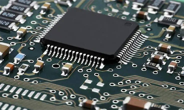
A Printed Wiring Board (PWB) is a type of circuit board that is composed of an epoxy glass substrate which is utilized to establish linkages to form an electrical circuit. PWB fabrication involves the creation of an electrical network over a substrate, where conductive paste is used to assemble the circuits. When it comes to creating an electrical connection, designers typically use a conductive plate during the design process.
PWB, which stands for printed wiring board, is a board employed by manufacturers to affix components and wire them together. This board is placed on top of a dielectric substrate and serves as a means for designers to link wires from one location to another. Printed Wiring Boards do not contain printed circuits, instead, during PWB fabrication, materials are etched away to develop conductive-isolating surfaces between traces. Manufacturers utilize plating through holes to link the conductive layers on a PWB, allowing for component installation and electrical connection.
Printed Wiring Boards (PWBs) do not contain any printed circuits, and serve as substrates without any components. During the manufacturing process of PWBs, materials are etched away to create conductive-isolating surfaces between traces, which is necessary for their function. In order to link conductive layers on a printed circuit board, manufacturers typically utilize plating through holes. These perforations not only facilitate installation of components, but also enable electrical connections to take place.
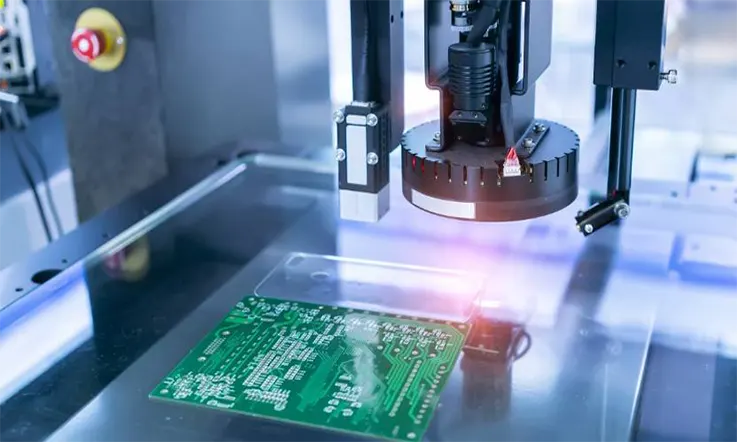
Fabrication Process of Printed Wiring Boards
The fabrication process of printed wiring boards typically includes the following steps:
● Material preparation: The process begins with the selection of the appropriate substrate material, usually fiberglass-reinforced epoxy. The substrate is then coated with a layer of copper on one or both sides to form the conductive pathways.
● Image etching: A resist material is applied to the copper layer, which is then exposed to ultraviolet light through the use of a patterned mask. The unexposed resist is then removed, leaving behind a patterned copper layer, essentially forming the circuit.
● Drilling and plating: Holes are drilled in the substrate for component leads and interconnections. The holes are then plated with a thin layer of copper to ensure electrical continuity.
● Solder mask and surface finishing: A solder mask is applied to the board to protect the exposed copper and prevent shorts. The board is then coated with a surface finish to protect it from environmental factors like oxidation and wear.
The fabrication process may also include additional steps such as lamination to create multi-layer boards, silk screening for labeling, and electrical testing to ensure functionality.
Printed Wiring Boards Advantage and Disadvantages
Advantages of Printed Wiring Boards:
● Reliable Connectivity: Printed wiring boards provide a reliable means of connectivity for electronic components, which leads to fewer failures and improved performance.
● Reduced Size and Weight: By using printed wiring boards, electronic systems can be made smaller and lighter, which is beneficial for the development of compact and portable devices.
● Efficiency: The use of printed wiring boards streamlines the electronic manufacturing process and reduces the need for wire harnesses, cables, and components, thereby improving the efficiency of the manufacturing process.
● Reproducibility: Printed wiring boards can be produced in large quantities, and the process can be tightly controlled to ensure consistent quality and performance.
● Cost-Effective: Printed wiring boards have a low manufacturing cost due to the efficiency and automation of the process.
Disadvantages of Printed Wiring Boards:
● Initial Design Cost: Printed wiring boards require designing and prototyping, which can be costly during the initial stages of product development.
● Limited Component Placement: The placement of components on printed wiring boards can be limited by the board’s size and layout, making it challenging to accommodate complex or specialized components.
● Difficult to Repair: Repairing printed wiring boards may be challenging, especially when dealing with multilayered boards, which may require specialized equipment.
● Environmental Concerns: The manufacturing process involves the use of chemicals and materials that can be harmful to the environment when not disposed of properly.
● Fragility: Printed wiring boards can be fragile and susceptible to damage during handling, transport, and assembly, which may affect their performance.
So, the advantages of printed wiring boards, such as reliable connectivity, reduced size and weight, and efficiency, outweigh the disadvantages such as environmental concerns, fragility, and the difficulty of repair. It is essential to weigh the advantages and disadvantages of printed wiring boards when deciding whether to use them in electronic devices.
Printed Wiring Boards (PWBs) Types
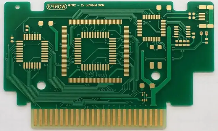
● Printed Wiring Boards (PWBs) can be categorized in a number of ways. One way is based on the complexity of the end product which is determined by the number of layers present. PWBs can be divided into three distinct groups based on the number of layers: single-sided, double-sided, and multilayer. Multilayer PWBs have more than two layers of circuitry, indicating that there is at least one layer beneath the surface of the circuit board.
A multilayer PWB may include as many interconnected layers as necessary, but most commonly have 4, 6, or 8 layers. Double-sided PCBs have only two interconnected layers, making them easier to manufacture compared to multilayer boards. Single-sided printed wiring boards have a layer of circuitry printed on one side of the substrate.
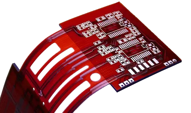
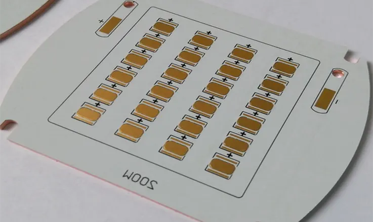
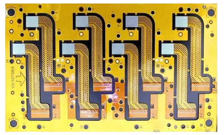
● Professionals also classify PWBs based on their substrate material and use. PWBs can be categorized as flexible, rigid, or rigid-flex, depending on their purpose. Flexible PWBs are made from substrates made of polyester and polyimide, and are able to maintain their flexibility making them suitable for a variety of applications. Flexible PWBs can be bent multiple times and can sustain a significant number of flexing cycles.
Rigid PWBs, on the other hand, are made from a glass-reinforced epoxy-resin by manufacturers. These PWBs are typically less than 0.1 inches thick. Rigid-flex PWBs combine the advantages of both rigid and flexible boards.
● Another way PWBs can be divided is based on the procedures used in their production. Both subtractive and additive processing are used. Subtractive processing involves carefully removing copper from a printed wiring board to create a circuit, followed by adding additional metals during the plating process. In subtractive processing, an image from a digital file is transferred to a copper circuit on a board using image transfer.
Additive processing, on the other hand, adds copper to a substrate to form the image. This process does not involve any etching or removal of copper. The additive process has been widely used for PWB manufacturing for a significant amount of time.
Testing and Inspection of Printed Wiring Boards
Testing and inspection are crucial steps in the manufacturing process of printed wiring boards to ensure that the final product meets the required quality standards. The following are the most commonly used methods for testing and inspection of printed wiring boards:
● Electrical testing: This method is used to verify the electrical connectivity of the boards. Automated testing equipment is used to apply electrical signals to each point on the board and compare the results against a predetermined set of parameters, such as resistance, voltage, and impedance.
● Visual inspection: This method involves a comprehensive examination of the board to check for any defects such as scratches, cracks, or misaligned components. Visual inspection can be conducted manually or with automated systems using optical cameras.
● X-ray inspection: This method is used to inspect the internal components of the board for any defects that cannot be detected by visual inspection. X-ray images can reveal issues such as solder bridging, insufficient soldering, or cracks in the substrate.
● Microsection analysis: This method involves taking a cross-sectional sample of a board for detailed microscopic analysis. It can provide valuable information about the quality of the plating and the bonding between layers in a multi-layer board.
● Thermal cycling: This test involves subjecting the board to a range of high and low temperatures to simulate the effects of thermal stress on the board. The board is inspected before and after the thermal cycles for any changes in its electrical or physical properties, such as delamination or cracking.
By using a combination of these testing and inspection methods, manufacturers can ensure that printed wiring boards meet the required quality standards and function reliably in their intended applications.
Applications of Printed Wiring Boards
Printed wiring boards, also known as printed circuit boards, have a wide range of applications in various fields. Some of the common applications of printed wiring boards include:
● Consumer electronics: Printed wiring boards are extensively used in a variety of consumer electronics, including smartphones, televisions, laptops, and gaming systems. They serve as a crucial component for the electrical connectivity of these devices.
● Industrial automation: Printed wiring boards are used in industrial automation systems, such as control panels, motor controls, and robotics. They help streamline the electrical connections and improve the overall performance of the system.
● Medical devices: Printed wiring boards are used in various medical devices, such as electrocardiogram machines, blood glucose meters, and patient monitors. These devices rely on printed wiring boards for reliable and accurate electrical connectivity.
● Aerospace and defense: Printed wiring boards are widely used in the aerospace and defense industries for applications such as navigation systems, satellite communications, and defense equipment. They provide a reliable means of electrical connectivity in harsh environments and demanding operating conditions.
● Automotive: Printed wiring boards are commonly used in automotive applications, such as engine control modules, navigation systems, and entertainment systems. They help reduce the size and weight of electrical systems, while improving their reliability and performance.
The above applications are just a few examples of where printed wiring boards are used. They are widely utilized in various other industries as well, such as telecommunications, energy, and transportation.
Factors of Influencing Printed Wiring Board Performance
The performance of a finished product is heavily reliant on the quality of the Printed Wiring Board (PWB) structure. PCB designers and assemblers must take a multitude of factors into consideration before creating the PWB. These considerations include numerous elements that must be carefully evaluated to ensure the desired level of performance is achieved.
Operational Speed
After the design and assembly process is complete, the currents in a printed wiring board (PWB) flow through the circuit’s traces, leading to the components and back again, powered by a power supply. Copper traces embedded in the board play a fundamental role in this function, and the substrate surrounding these traces can have an impact on signal strength and speed.
The substrate material negatively affects the time it takes for a signal to travel from one location to another, also known as “time of flight.” This impact is mathematically expressed as an inverse proportion to the square root of the dielectric constant of the substrate material. Simply put, the signal will face more resistance if the substrate is thicker and less conductive.
The length of conductors traversed by the signal also affects the time it takes for it to travel. Assemblers are required to use shorter conductors to create designs that are both brief and quick. If the desired performance is greater than 25 MHz, then strip lines and micro-strips can be used as a supplement to the conductors in order to improve performance.
Power Consumption
Power consumption is a critical concern when it comes to fabricating printed circuit board assemblies. Issues with power consumption can arise as early as the PWB stage. The amount of power required to run a circuit is directly proportional to the number of gates present. When developing a PWB, it is necessary to consider the appropriate power supply and adjust the number of gates and clock rate accordingly.
In addition, when high-speed switching circuits are involved, it is crucial to consider the ground return current flow of the traces. Without sufficient grounding, switched circuits can quickly cause overheating, burnout, or disruptions in the flow of current.
If a board has multiple layers, it becomes necessary to include a ground plane between each of the layers to maintain low resistance. These ground planes function as extensive grounding regions that efficiently scatter the return current.
Thermal Management
Printed Wiring Boards (PWBs) are typically poor heat conductors. The substrate material’s ability to absorb and retain heat necessitates the incorporation of additional heat-dissipating mechanisms in PWB designs to prevent excessive temperatures from developing.
FR4 is an ideal substrate material for most circuits as it can absorb a reasonable amount of heat. However, high-speed circuits require significantly better thermal management capacity. Fortunately, there are several approaches to achieve this goal. These include:
● Heat Vias: Heat vias, also known as thermal vias, are small holes present on a circuit board lined with a conductive material to allow heat to escape from the board. In addition, the air surrounding the board can help dissipate the heat.
● Heat Sinks: Heat vias or thermal vias are designed to remove heat from the printed circuit board, allowing it to dissipate without damaging the circuit.
● Conductive Planes: Conductive planes are layers of conductive material deposited between two layers of a board, typically employed with multilayer boards. They are capable of safely distributing the heat generated by the surrounding boards, as they can absorb heat and release it across a larger area.
Incorporating these components into the PWB design can enhance heat management, current, and component utilization. The choice of approach depends on the number of PCB layers and the PCB layout.
Printed wiring boards (PWBs) are a vital component in the printed circuit board (PCB) assembly process. Designing these components is just as important as planning for the product as a whole. A poorly designed PWB will result in a PCB with poor design. Therefore, it is crucial to consider the quality of the PWB when choosing a partner for PCB assembly.
What Is the Difference Between PWB and PCB ?
Printed Wiring Boards (PWB) and Circuit Boards are two distinct types of boards, and their differences are as follows:
● Electrical Components: When comparing Printed Circuit Boards (PCBs) to Printed Wiring Boards (PWBs), one of the main and significant differences is that a PCB refers to a board that already contains the entire circuitry, while PWBs consist of a board without any components.
This fundamental distinction signifies that PCBs are essentially finished versions of circuit boards and are ready for use in various electronic products. On the other hand, the use of PWBs is useful in identifying the initial stages of circuit board creation, as well as demonstrating the usefulness of circuit boards in electronics, which do not require highly complex capabilities.
● Area and Location: The terms “Printed Wiring Board” and “Printed Circuit Board” can be used interchangeably in the context of the electronics manufacturing industry in the United States, depending on the region or place.
During the early stages of the electronics industry, the term “Printed Wiring Board” was widely used, as the connections present on the boards were primarily from one point to another. Later, when the technology of circuit boards had advanced significantly, the term “circuit” became more appropriate due to the complex functionalities offered by printed circuit boards. Initially, this term was only used for internal purposes, but it eventually gained widespread use.
Printed wire boards, also known as design substrates, are limited to the preproduction of electronic devices, as the technological breakthroughs have made PCBs available to the general public. Printed wire boards have no components attached to them, and their design includes openings for the soldering of electrical components both into and through the components themselves.
Before the necessary electronic components can be attached to printed circuit boards, printed wiring boards must undergo a series of chemical and physical procedures.
Additional Terms That Are Associated with PWB and PCB
In addition to PCB and PWB, other common terms used in reference to printed circuit boards include PCBA, CCA, PCA, and PWA.
PCBA stands for Printed Circuit Board Assembly, referring to the process of assembling a printed circuit board. This term has been widely used since the shift in 1999 and is preferred by both users and technical committees.
● PWA, or Printed Wire Assembly, is an obsolete term for printed circuit board assembly and is now rarely used.
● CCA, or Circuit Card Assembly, is another term used to refer to the assembled circuit board. While it refers to the same substance as PCBA, CCA is not a widely used term.
● PCA, or Printed Circuit Assembly, is essentially the same as PCBA but is not commonly used nowadays.
As a result, PWB, PCB, and Circuit Cards all refer to the bare printed circuit board, while PCA, CCA, PWA, and PCBA refer to the assembled circuit board. PCB and PCBA are the most commonly used terms out of these options.
PWB Manufacturers Types
The production of PWBs is a complex and technically demanding process that requires significant pieces of machinery. Companies in the PWB industry design these boards for various purposes, and the level of competition in this sector is extremely high. The manufacturers of printed wiring boards can be categorized into two groups: independent and captive manufacturers.
● Independent manufacturer: Independent PWB manufacturers specialize in creating printed wiring boards for integration into electronic goods, and the industry is characterized by fierce competition among various regional manufacturers. These companies engage in cutthroat competition to win contracts from a diverse range of clients, manufacturing PWBs for sale on the open market. To secure a contract, an independent PWB manufacturer typically submits a proposal highlighting their ability to meet a customer’s specific product requirements.
● Captive manufacturer: The term “Original Equipment Manufacturer” (OEM) is sometimes used to refer to captive manufacturers who create their own printed wiring boards (PWBs) to produce electronic devices. However, this type of manufacturer is relatively rare in the global market. Unlike independent manufacturers, OEMs do not produce printed circuit boards (PCBs) for distribution on the open market and instead focus on creating their own electronic products.
Conclusion
Printed wiring boards are an essential component in modern electronic devices across various industries. They enable reliable electrical connectivity, streamline the manufacturing process, and reduce the size and weight of electronic systems. With advancements in technology, printed wiring boards are becoming more complex and efficient, with the ability to accommodate smaller components and improved electrical and mechanical performance. The manufacturing process involves several stages, including material preparation, etching, drilling, and inspection, to ensure high quality and reliable performance.
This article provides a comparison between PWB and PCB, the two commonly used types of circuit boards used in electronic devices. While both terms share similarities, there are also distinct differences between them. Despite this, both types of boards offer support for various technologies and products across a broad range of industries. It is worth noting that preferences for the use of PWB or PCB may differ depending on geographic location.