
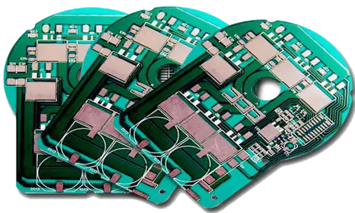
As the electronics industry continues to focus on sustainability and high-performance standards, halogen free PCB have emerged as a key solution. These eco-friendly circuit boards offer a smart alternative to traditional options by eliminating harmful substances like bromine and chlorine, aligning with both environmental regulations and health-conscious trends. The development of halogen-free PCBs marks a significant milestone, addressing the growing need for greener electronics without compromising on quality or performance.
This guide delves into the evolution, design, manufacturing, and benefits of halogen-free PCBs, shedding light on the cutting-edge innovations and the future potential of this technology.
Historical Perspective: The Rise of Halogen-Free Materials
The evolution of printed circuit boards (PCBs) has witnessed many technological shifts, with one of the most notable being the adoption of halogen-free materials. In the early days of PCB manufacturing, materials rich in halogens such as bromine and chlorine were commonly used in flame-retardant components. However, as environmental awareness grew, concerns over the release of harmful toxins from these halogens during the burning or incineration of waste materials led to a reevaluation of their use.
The introduction of halogen-free PCBs was a response to stringent environmental regulations like the RoHS directive, which aimed to limit hazardous substances in electronic products. Manufacturers began to explore alternative materials that could maintain the same level of performance without the environmental and health risks associated with halogenated flame retardants.
From Compliance to Innovation
Initially, halogen-free PCBs were primarily seen as a necessity for compliance with environmental laws. However, over time, engineers and manufacturers realized that halogen-free materials could provide not only environmental benefits but also performance enhancements. Innovations in material science have led to halogen-free PCBs that not only meet RoHS and WEEE standards but also offer improved thermal stability, signal integrity, and long-term reliability.
The shift from a compliance-driven mindset to one focused on innovation has been pivotal in shaping the landscape of modern PCB design and manufacturing. By leveraging new materials such as low-smoke halogen-free resins and green laminates, we can now produce high-performance circuit boards that support the demands of advanced electronics in a variety of industries.
Market Drivers
The rise in demand for halogen-free PCBs can be attributed to several key drivers. Environmental sustainability, health concerns, and regulatory pressures are the primary factors that have accelerated the adoption of these materials. Moreover, industries such as automotive, medical devices, telecommunications, and consumer electronics are increasingly favoring halogen-free solutions for their environmental benefits and compliance with global standards.
What Are Halogen-Free PCBs?
Halogen-free PCBs represent a shift toward safer and more sustainable electronics manufacturing. These circuit boards eliminate or drastically reduce halogenated flame retardants, meeting specific thresholds that align with environmental and health standards.
Defining Halogen-Free Materials
Halogen-free materials are designed to replace brominated and chlorinated compounds commonly used as flame retardants in traditional PCBs. These compounds, while effective, release toxic gases during combustion, posing risks to human health and the environment.
To qualify as halogen-free, a material must adhere to stringent limits:
●Bromine (Br) content must be less than 900 parts per million (ppm).
●Chlorine (Cl) content must also stay below 900 ppm.
●The combined total of halogens must not exceed 1500 ppm.
This threshold, set by standards such as IEC 61249-2-21, ensures these boards meet fire safety requirements without relying on halogenated chemicals. Alternative materials, such as phosphorus-based compounds and mineral fillers, provide the needed flame-retardant properties.
| Property | Halogen-Free Materials | Traditional Halogenated Materials |
| Flame Retardant | Phosphorus-based | Brominated epoxy resin |
| Environmental Impact | Low toxicity | High toxicity in combustion |
| Threshold Limit | <1500 ppm total halogens | No specified limit |
For example, manufacturers producing PCBs for wearable medical devices often prefer halogen-free materials to minimize emissions during disposal, aligning with their focus on health-conscious design.
Key Characteristics of Halogen-Free PCBs
Switching to halogen-free PCBs impacts both the materials used and the overall performance of the boards. These boards exhibit unique properties that differentiate them from their traditional counterparts:
1.Enhanced Flame Resistance-
●While traditional brominated flame retardants work through chemical halogenation, halogen-free PCBs use alternative compounds like phosphorus derivatives. These compounds char at high temperatures, creating a protective barrier that slows down combustion.
2.Improved Thermal Stability-
●Halogen-free PCBs typically feature higher glass transition temperatures (Tg), ranging between 170–200°C, making them suitable for high-performance applications such as 5G and automotive electronics.
3.Electrical Performance-
●Halogen-free materials boast lower dielectric constants (Dk) and dissipation factors (Df), improving signal integrity in high-speed and high-frequency circuits.
| Metric | Halogen-Free PCBs | Traditional PCBs |
| Dielectric Constant | ~3.5-4.5 | ~4.5-5.5 |
| Dissipation Factor | ~0.002-0.005 | ~0.008-0.015 |
| Glass Transition Temp | 170–200°C | 140–170°C |
In a high-speed server application, using halogen-free PCBs reduces electromagnetic interference (EMI) while ensuring stable data transmission, proving their worth in cutting-edge tech designs.
Pro Tip: Don’t let old-school materials bog you down. Upgrade to halogen-free boards and watch your high-speed designs hit new benchmarks.
Regulatory Standards for Halogen-Free PCBs
When it comes to manufacturing or sourcing halogen-free PCBs, navigating the maze of regulations and industry standards is no small feat. Various global directives outline what qualifies as halogen-free and specify how these boards should be marked, handled, and disposed of in an environmentally responsible manner. These rules are not only about ensuring that the products meet safety and environmental requirements but also about staying compliant with an increasing push for eco-friendly alternatives.
1.RoHS and WEEE Compliance-
The Restriction of Hazardous Substances (RoHS) directive bans the use of certain hazardous materials, including halogens, in electronic products. Meanwhile, the Waste Electrical and Electronic Equipment (WEEE) directive encourages recycling and proper disposal, minimizing environmental harm.
2.IEC 61249-2-21 Standards-
The IEC 61249-2-21 defines the specific requirements for halogen-free materials, ensuring uniformity across manufacturers. Boards complying with this standard are labeled as safe for environmental applications.
For example, a European-based electronics manufacturer seeking to distribute globally must align with both RoHS and IEC 61249-2-21 standards to avoid hefty penalties and market restrictions.
| Regulation | Requirement |
| RoHS | Limits hazardous substances in electronics |
| WEEE | Mandates recycling and responsible disposal |
| IEC 61249-2-21 | Specifies halogen content limits and safety metrics |
Benefits of Using Halogen-Free PCBs
The adoption of halogen-free PCBs signals a shift towards more responsible and innovative engineering practices. These boards not only address environmental challenges but also offer advanced performance benefits and compliance with stringent safety standards. Below, we delve deeper into their multi-faceted advantages.
Environmental Advantages
Halogen-free PCBs provide a greener alternative for the electronics industry, addressing the growing concern over e-waste and its environmental impact.
1.Minimized Release of Harmful Emissions-
During combustion or improper disposal, traditional PCBs with brominated flame retardants release dioxins and furans, which are persistent organic pollutants. Halogen-free materials minimize these emissions, reducing the impact on air quality and public health.
Example: Countries with stringent environmental policies, such as Germany and Japan, have reported lower incidences of environmental contamination due to increased adoption of halogen-free alternatives.
Material Emission Comparison:
| Material | Emission Type | Environmental Impact |
| Brominated PCBs | Dioxins, Furans | High |
| Halogen-Free PCBs | Carbon-based Byproducts | Low |
2.Supporting Global Initiatives-
Companies that adopt halogen-free PCBs align with global environmental goals like the European Union’s RoHS (Restriction of Hazardous Substances) directive. These boards facilitate compliance, ensuring businesses stay ahead of regulatory demands.
Performance Benefits
Halogen-free PCBs offer more than just environmental benefits—they’re packed with high-performance capabilities that make them stand out in demanding applications. These boards boast exceptional material properties, ensuring they hold up under stress and provide long-lasting durability. They’re designed to meet the needs of high-tech industries, whether it’s in IoT devices, automotive systems, or wearable tech.
1.Enhanced Dielectric Properties-
With lower dielectric constants, halogen-free materials reduce signal loss in high-frequency applications, ensuring smoother data transmission in devices such as 5G networks and advanced automotive sensors.
2.Heat Resistance and Stability-
Halogen-free PCBs have higher glass transition temperatures (Tg), allowing them to operate in more extreme conditions without compromising functionality. This makes them an ideal choice for sectors like aerospace and telecommunications.
3.Chemical Stability in Harsh Environments-
In industries like oil and gas, where exposure to chemicals is inevitable, halogen-free PCBs resist degradation better than their traditional counterparts.
Industry and Consumer Safety
Safety goes beyond simply adhering to regulations—it’s about designing products that users can depend on under any circumstances. By focusing on quality materials and thorough design practices, we can create products that perform reliably, even in demanding real-world conditions. This approach ensures that users can trust the performance of the product, whether it’s used daily or in high-stakes situations.
1.Reduced Fire Hazards-
Traditional PCBs containing halogens can release toxic gases when exposed to fire, exacerbating risks for both users and first responders. Halogen-free materials produce safer emissions, offering peace of mind in fire scenarios.
2.Compliance with Safety Standards-
Halogen-free PCBs meet rigorous international safety benchmarks, including UL 94-V0 flame retardancy and IEC 61249-2-21 specifications. These certifications ensure that products are not only safer but also globally marketable.
3.Improved Workplace Safety-
Factories handling halogen-free materials report lower risks of toxic exposure during manufacturing, making the switch a win for worker health and safety.
Example: A consumer electronics company launched a line of smartphones with halogen-free PCBs and saw an uptick in eco-conscious customers, driving brand loyalty.
The Complexities and Challenges in Designing Halogen-Free PCBs
The design of halogen-free PCBs presents unique opportunities and obstacles, demanding a fine balance of material science, engineering precision, and cost management. This section discussion expands on key challenges and practical approaches to address them while embedding real-world examples and expert insights.
Overcoming Material Limitations in High-Performance Designs
While halogen-free materials offer numerous benefits, designing high-performance halogen-free PCBs comes with its own set of challenges. Many halogen-free resins and laminates tend to have different physical properties compared to their halogenated counterparts, which can impact factors such as thermal conductivity, dimensional stability, and electrical performance. For instance:
1.Thermal Conductivity and Electrical Performance-
Halogen-free laminates often display lower thermal conductivity, impacting heat dissipation in densely packed designs. Dimensional stability under stress is another concern, as high-temperature cycles may introduce warping or delamination. These issues are especially pronounced in PCBs for automotive and aerospace applications.
●Practical Insight: Engineers working on high-speed designs often encounter signal integrity challenges due to the dielectric constant variations in halogen-free materials. This might require additional compensatory design techniques, such as tweaking trace geometry or implementing advanced signal isolation methods.
Case Study Table: Material Properties
| Material | Dielectric Constant (Dk) | Thermal Conductivity (W/mK) | Application Notes |
| Halogen-Free Epoxy Resin | 3.6-3.8 | 0.3-0.5 | Suitable for moderate-speed PCBs |
| Brominated FR4 | 4.2-4.5 | 0.4-0.6 | Common for general-purpose designs |
When selecting materials for a particular application, it’s important to consider both the specific requirements and performance standards without making compromises. For example, in high-speed PCB designs, ensuring signal integrity can be a tough challenge, especially when working with certain halogen-free laminates. These materials may require extra attention to detail to prevent issues that could affect the performance of the board in high-frequency environments
Compensating for Thermal Properties in Halogen-Free PCBs
Another challenge in the design of halogen-free PCBs is managing their thermal properties. Halogen-free materials may exhibit different thermal expansion coefficients (CTEs), which can lead to issues with thermal stress and component reliability in high-temperature environments. Special attention must be given to heat dissipation, especially in applications where high-frequency signals and high temperatures are involved, such as in automotive electronics or telecommunications equipment.
Therefore, effective thermal management is non-negotiable when using halogen-free materials, especially in applications demanding high reliability.
1.Thermal Expansion and Stress-
Halogen-free PCBs often exhibit different Coefficients of Thermal Expansion (CTEs), potentially causing issues during reflow soldering or thermal cycling. This can impact solder joint reliability, especially in multilayer boards with high aspect ratio vias.
2.Heat Dissipation in High-Frequency Applications-
Applications such as 5G infrastructure or radar systems push the limits of thermal stability. We must implement heat-sink strategies, such as using thicker copper layers, integrating thermal vias, or selecting resins with enhanced thermal properties.
Example: A leading telecom manufacturer used advanced halogen-free laminates with copper-filled vias to improve heat conduction in a 5G antenna PCB, reducing operating temperatures by 12%.
Overcoming Cost Barriers in Halogen-Free PCB Design
Cost is often cited as a barrier to adopting halogen-free PCBs, as the materials tend to be more expensive than traditional halogenated alternatives. However, the long-term benefits in terms of environmental sustainability and regulatory compliance can offset these initial costs. Additionally, as demand for halogen-free solutions increases, economies of scale are expected to reduce the cost of production, making these materials more accessible to a broader range of manufacturers.
1.Cost Considerations-
Manufacturers often cite a 10-15% cost premium for halogen-free materials. This upfront investment, however, can be balanced by regulatory compliance, reduced environmental taxes, and market preference for greener products.
2.Economies of Scale in Manufacturing-
As halogen-free PCBs gain traction in industries like consumer electronics and automotive, the supply chain for these materials is improving. Bulk production has led to more competitive pricing, benefiting manufacturers and consumers alike.
Industry Data Comparison:
| Type | Material Cost (per sq. ft.) | Processing Cost | Market Trends |
| Standard Halogenated PCB | $0.50-$0.80 | Moderate | Stable demand |
| Halogen-Free PCB | $0.60-$1.10 | Slightly Higher | Growing adoption |
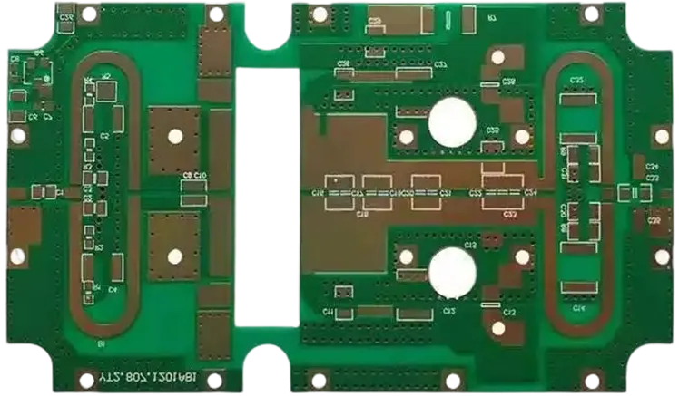
Advanced Design Strategies for Halogen-Free PCBs
The push towards halogen-free PCBs demands innovative approaches to balance environmental responsibility with technical performance. Designers must employ strategic material selection, stackup optimization, and thermal management to ensure that these PCBs meet industry demands. Below is an exploration of these strategies with actionable insights and real-world examples.
Material Selection for Performance
Choosing the right materials is a cornerstone of halogen-free PCB design. These materials, often utilizing phosphorus- or nitrogen-based flame retardants, deliver flame resistance without compromising environmental goals.
1.Properties to Consider-
Halogen-free laminates often come with higher glass transition temperatures (Tg) and better fire resistance. However, these materials might show some differences in terms of dielectric constants and thermal conductivity when compared to their traditional counterparts. For designs that demand high speeds or high frequencies, these factors can impact how well the board handles signal transmission.
Halogen-Free vs. Halogenated Laminates:
| Property | Halogen-Free Materials | Halogenated Materials |
| Glass Transition (Tg) | Higher (>150°C) | Moderate (120°C-140°C) |
| Dielectric Constant | 3.5-4.0 | 4.2-4.8 |
| Thermal Conductivity | Lower (0.3-0.5 W/mK) | Moderate (0.4-0.6 W/mK) |
2.Selection Tips-
●For automotive applications, consider laminates with excellent thermal stability to withstand prolonged high-temperature exposure.
●For high-frequency PCBs, prioritize materials with low dielectric loss to maintain signal clarity.
Optimizing PCB Stackup
Designing an effective stackup is key when working with halogen-free PCBs. A carefully planned stackup not only boosts overall performance but also makes the manufacturing process more efficient and manageable.
1.Layering Strategies-
●Signal Integrity: Place ground planes close to signal layers to minimize crosstalk and electromagnetic interference (EMI).
●Thermal Management: Use power planes as thermal spreaders to improve heat dissipation, especially for components with high power consumption.
2.Balancing Complexity and Manufacturability-
Designs with numerous layers can complicate manufacturing. For halogen-free boards, it’s essential to ensure that the laminate layers maintain cohesion under thermal and mechanical stresses.
8-Layer Halogen-Free PCB Stackup:
| Layer | Purpose |
| 1 | Signal |
| 2 | Ground Plane |
| 3 | Power Plane |
| 4 | Signal |
| 5 | Signal |
| 6 | Power Plane |
| 7 | Ground Plane |
| 8 | Signal |
Thermal Management Techniques
Thermal management is non-negotiable in halogen-free PCBs. Without halogens, some materials may have lower thermal conductivity, making heat dissipation strategies even more essential.
1.Using Heat Sinks and Thermal Vias-
Integrating heat sinks and thermal vias effectively pulls heat away from sensitive components. For instance, in a power amplifier PCB, a grid of thermal vias can channel heat to an attached heatsink or thermal pad.
2.Copper Layout Techniques-
Wider copper traces and heavier copper weights distribute heat more evenly. Considerations for copper distribution are critical in PCBs for telecommunications, where components operate under sustained high loads.
Application: A major IoT manufacturer employed halogen-free materials with 2-ounce copper layers and optimized via placement, reducing device operating temperatures by 15% without compromising compact design requirements.
Signal Integrity and High-Speed Design for Halogen-Free PCBs
High-speed PCB design requires a deep understanding of signal integrity, as any loss or distortion in signals can affect the performance and reliability of electronic systems. This challenge is compounded when using halogen-free materials, which have unique dielectric properties that may impact signal quality in high-frequency applications. We must adopt advanced strategies to mitigate issues like signal loss, crosstalk, and interference when designing with halogen-free PCBs.
Material Impact on Signal Loss
The dielectric properties of PCB materials play a key role in determining how well the board maintains signal quality, especially in high-speed designs. Dielectric constant (Dk) and dissipation factor (Df) are two crucial properties that influence signal transmission. When selecting materials for halogen-free PCBs, it’s important to choose ones that exhibit a low Dk and a minimal Df to reduce signal degradation over long distances or high-frequency ranges.
●Dielectric Constant (Dk)-
A high Dk leads to increased signal loss, particularly at higher frequencies. Halogen-free materials often exhibit slightly higher Dk values compared to traditional halogenated PCBs, which can result in greater signal attenuation.
Example: A PCB material with a Dk value of 4.5 might cause more signal loss than a material with a Dk of 3.5, especially at gigahertz frequencies.
●Dissipation Factor (Df)-
The Df reflects how much energy is lost as heat during signal transmission. Halogen-free materials generally offer lower Df, making them suitable for maintaining higher signal integrity over long distances.
| Material Type | Dielectric Constant (Dk) | Dissipation Factor (Df) |
| Standard FR-4 | 4.2 – 4.7 | 0.02 – 0.03 |
| Halogen-Free Materials | 3.5 – 4.5 | 0.015 – 0.025 |
Best Practices for High-Frequency PCB Designs
High-frequency PCBs require careful layout strategies to minimize signal degradation caused by factors like crosstalk, interference, and ground bounce. Here are several best practices to optimize signal integrity in halogen-free PCBs:
1.Use of Controlled Impedance Routing: To maintain signal integrity, controlled impedance traces are a must. By ensuring that trace widths are consistent and match the desired impedance, we can minimize reflections and signal loss. The impedance must also be matched to the component’s specifications to avoid performance issues.
2.Minimize Crosstalk: Crosstalk happens when signals from adjacent traces start messing with each other, a real headache, especially at high frequencies. To keep this under control, you need to:
●Increase the spacing between traces carrying high-speed signals.
●Use ground planes to shield signal traces.
●Route high-speed signals on different layers to keep them physically separated.
3.Optimizing Ground and Power Planes: Using solid ground and power planes helps reduce noise and provide a stable signal reference. For halogen-free PCBs, adding multiple layers of ground and power planes can further enhance signal stability and improve the overall performance of the board
4.Use of Via-in-Pad Technology: In high-speed designs, via-in-pad technology helps to reduce the length of signal paths and can contribute to better signal quality. This is especially effective in halogen-free PCBs where more complex routing is required.
Testing Signal Performance
Once the design is finalized, ensuring the signal integrity of halogen-free PCBs requires thorough testing. We must rely on a range of tools and methodologies to evaluate the performance of these boards, ensuring that they meet the stringent requirements of high-speed applications.
1.Time Domain Reflectometry (TDR): TDR is a powerful tool used to test the integrity of high-speed signals by analyzing how a signal is reflected back when transmitted through a PCB trace. By observing reflections and identifying signal losses or impedance mismatches, TDR helps ensure that the design is free from faults that could degrade signal quality.
2.Network Analyzers: These devices measure the network parameters of the PCB, such as S-parameters, to analyze the board’s response to high-frequency signals. This allows designers to see how well the PCB performs in terms of attenuation, return loss, and other key signal integrity factors.
3.Simulation Software: Before testing a physical prototype, simulation software such as Ansys HFSS or Keysight ADS can be used to predict how signals will behave on the PCB. Simulations help to identify potential issues early in the design phase, enabling us to optimize the layout for signal integrity before fabrication begins.
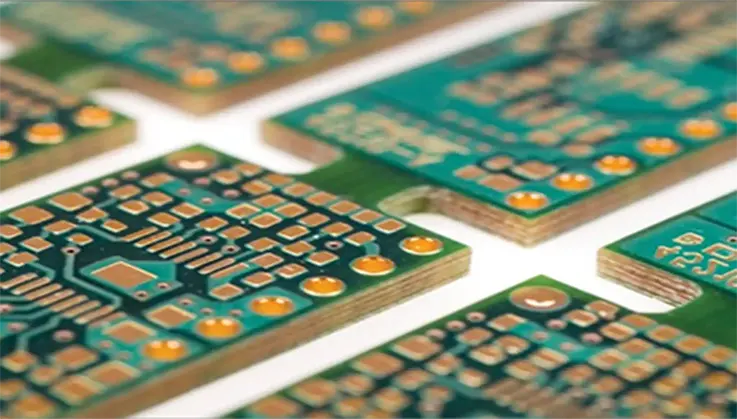
Halogen-Free PCB Manufacturing: Innovations and Processes
The manufacturing of halogen-free PCBs involves innovative processes and adjustments tailored to the unique material properties and environmental goals of these boards. Below is an exploration of key areas in this manufacturing domain.
Advanced Lamination Techniques for Halogen-Free PCBs
Lamination is a critical process in the manufacturing of halogen-free PCBs, as it ensures the proper bonding of layers and the overall mechanical integrity of the board. Advanced lamination techniques are required to handle the specific properties of halogen-free materials, which often have different curing and bonding characteristics than conventional materials.
Technologies such as high-pressure lamination and vacuum lamination are employed to enhance the performance of halogen-free PCBs, ensuring better layer adhesion, thermal stability, and electrical conductivity.
1.High-Pressure Lamination-
By applying controlled pressure during the curing process, high-pressure lamination enhances the bonding strength between layers, especially for halogen-free materials that may have reduced adhesion compared to halogenated counterparts. This technique minimizes risks such as delamination or warping in multi-layer boards.
2.Vacuum Lamination-
Vacuum lamination reduces air entrapment during layer bonding. This method is particularly advantageous for halogen-free PCBs, as it ensures consistent layer uniformity and eliminates voids, which can compromise the board’s thermal and electrical properties.
3.Process Optimization-
Advanced temperature and pressure profiles are often employed to match the specific requirements of halogen-free materials. For example, laminates with phosphorus-based flame retardants typically require higher curing temperatures to achieve desired performance characteristics.
Example:
| Laminate Type | Curing Temperature | Pressure Range | Cycle Time |
| Standard Halogen-Free | 180°C-200°C | 350-400 psi | 60-90 minutes |
| High-Tg Halogen-Free | 200°C-220°C | 400-450 psi | 90-120 minutes |
Soldering and Assembly Considerations in Halogen-Free PCBs
Soldering halogen-free PCBs presents specific challenges due to the differences in their wetting properties compared to traditional boards. These boards often require extra care to ensure strong solder joints and reliable performance. To tackle this, we must use specialized soldering methods, such as lead-free solder and fine-tuned reflow profiles, to guarantee that components securely bond to the PCB. If not done correctly, poor solderability can lead to defects, affecting the functionality and longevity of the board. By following these tailored techniques, we can ensure the integrity of the final assembly, paving the way for durable and high-performing devices.
1.Wetting Properties-
Halogen-free materials may not exhibit the same solder spread as traditional laminates. To overcome this, solder paste formulations and flux compositions can be adjusted to achieve optimal wetting and adhesion.
2.Lead-Free Soldering-
Lead-free solder, a common requirement in halogen-free PCB assembly, typically involves higher melting points. PCB Assembly factory must adapt their reflow profiles to accommodate these requirements without causing thermal damage to components.
3.Process Enhancements-
Nitrogen reflow atmospheres can reduce oxidation during soldering, improving joint reliability. Additionally, inspection technologies, such as X-ray analysis, help verify solder joint integrity in complex assemblies.
Automation and the Future of PCB Manufacturing
Automation is reshaping PCB manufacturing, particularly for halogen-free boards. Automated systems like pick-and-place, inspection, and testing boost efficiency, accuracy, and scalability in production. As technology keeps improving, these advancements are helping bring down costs while enhancing quality. This makes halogen-free PCBs more accessible and easier to integrate into large-scale production. By streamlining processes, automation tackles the unique challenges of working with these materials, ensuring consistent results and faster turnaround times. In short, automation is helping manufacturers keep up with demand while improving the overall production process.
1.Pick-and-Place Systems-
●High-speed pick-and-place machines equipped with vision systems allow for precise placement of components, which is especially beneficial for the dense layouts found in halogen-free PCBs used in IoT and wearable devices. These machines ensure that each component is positioned accurately, enhancing the performance and reliability of the final product.
2.Automated Optical Inspection (AOI)-
●AOI systems detect surface-level defects, such as misaligned components or solder bridges, ensuring quality assurance in every production run.
3.Scalability through Automation-
●Automation not only streamlines production but also enhances scalability, enabling PCB manufacturers to meet rising demand for halogen-free PCBs in industries such as automotive and 5G telecommunications.
Challenges in Manufacturing Halogen-Free PCBs
The manufacturing of halogen-free PCBs introduces a unique set of hurdles that require innovation and meticulous planning. These challenges, ranging from material sourcing to process adaptation and quality assurance, demand careful navigation to ensure the production of high-performing, reliable PCBs. Here’s a closer look:
Material Sourcing and Costs
The availability and pricing of halogen-free laminates represent a primary concern for manufacturers. These materials often include phosphorus- or nitrogen-based flame retardants, which differ significantly from conventional halogenated counterparts in terms of sourcing complexity and production costs.
1.Availability-
●Halogen-free materials are not yet as widely produced as traditional options, which can lead to limited supplier choices. Global supply chain disruptions further exacerbate this issue, causing delays and increasing lead times.
2.Cost Factors-
●Higher manufacturing costs for halogen-free materials often stem from specialized production requirements.
●Manufacturers must weigh these costs against performance needs, particularly for applications requiring stringent environmental compliance or advanced electrical properties.
Example Scenario:
| Material Type | Price per Sheet (USD) | Typical Use Case |
| Standard FR-4 | $8 – $12 | General consumer electronics |
| Halogen-Free FR-4 | $15 – $20 | Eco-friendly devices |
| High-Tg Halogen-Free FR-4 | $25 – $35 | Automotive, telecom |
Adaptations in Manufacturing Processes
Manufacturing processes for halogen-free PCBs require adjustments to accommodate the unique properties of these materials. These changes impact lamination, drilling, soldering, and high-temperature processing.
1.Lamination Adjustments-
●Higher curing temperatures and controlled pressure cycles are necessary to achieve proper bonding of halogen-free laminates, which often feature different thermal expansion coefficients.
●Vacuum-assisted lamination helps reduce voids, ensuring uniformity across layers.
2.Drilling Considerations-
●Halogen-free laminates tend to be more brittle, which can lead to issues such as cracking or delamination during drilling. PCB Manufacturers may use diamond-coated drill bits and slower spindle speeds to mitigate these risks.
3.Soldering Techniques-
●Lead-free soldering, paired with optimized reflow profiles, ensures strong and reliable connections. Nitrogen reflow environments help minimize oxidation and improve solder joint quality.
Practical Tip: Regular calibration of equipment and process trials are recommended to maintain consistency and reduce defect rates when switching to halogen-free materials.
Quality Control and Testing
Ensuring the long-term reliability of halogen-free PCBs requires rigorous quality control measures and testing protocols tailored to their unique mechanical and environmental properties.
1.Mechanical Testing-
●Conduct peel strength tests to assess the adhesion of copper traces. Halogen-free materials may have varying levels of adhesion compared to conventional laminates.
●Perform flexural strength tests to evaluate the board’s ability to withstand mechanical stress during assembly and operation.
2.Environmental Testing-
●Temperature cycling tests simulate real-world conditions, especially for applications in harsh environments like automotive or aerospace.
●Conduct humidity and thermal shock tests to evaluate the board’s resistance to moisture ingress and rapid temperature changes.
Example Table:
| Test Type | Parameter | Purpose |
| Peel Strength | ≥ 1.5 N/mm | Assess copper trace adhesion |
| Thermal Cycling | -40°C to 125°C, 500 cycles | Simulate environmental stress |
| Humidity Resistance | 85°C, 85% RH, 72 hours | Evaluate moisture ingress |
Halogen-Free PCB vs. Halogen-Containing PCB Materials
Understanding the differences between halogen-free and halogen-containing PCB materials helps manufacturers and engineers make informed decisions. These differences influence material properties, costs, production challenges, and the performance and environmental impact of the final products.
Cost Dynamics: Halogen-Free Materials Come at a Premium
The financial aspect is one of the most noticeable distinctions between halogen-free and halogen-containing materials. Producing halogen-free PCBs involves using specialized resins, typically phosphorus or nitrogen-based flame retardants. These materials are more expensive due to their composition and the advanced manufacturing processes they require.
| Material Type | Approx. Cost Increase | Reason for Cost Difference |
| Halogen-Containing FR-4 | Baseline | Widely available and standardized production processes |
| Halogen-Free FR-4 | +20%-50% | High material toughness, stricter process requirements |
Example: The toughness of halogen-free materials often demands more robust equipment for drilling and machining, which can add to production costs. Moreover, the additional expense is also reflected in waste reduction strategies needed for environmentally compliant manufacturing.
Physical Properties and Longevity Trade-offs
Halogen-free materials exhibit distinct physical properties that influence the lifespan and mechanical characteristics of the PCBs. While their eco-friendly composition reduces environmental harm, the inherent toughness of these materials can create challenges during the manufacturing and operational phases.
●Mechanical Challenges: Halogen-free laminates are generally harder, which makes them more difficult to drill or cut. This can impact precision during fabrication, leading to a potential reduction in production yields.
●Reduced Lifespan: Studies show that the lifespan of halogen-free PCBs may decrease by about 20%-30% in high-stress applications due to material rigidity and thermal expansion differences.
| Attribute | Halogen-Containing Materials | Halogen-Free Materials |
| Flexibility | Moderate | Lower due to material toughness |
| Thermal Expansion | Balanced across layers | Higher in specific directions |
| Environmental Compliance | Limited | High |
Manufacturing Complexity and Costs
The fabrication of halogen-free PCBs involves additional steps to maintain the required mechanical and electrical properties. These extra processes naturally contribute to higher production costs.
●Lamination Process Adjustments: Halogen-free materials often require higher temperatures and pressures during the lamination process. Vacuum-assisted lamination is frequently used to ensure even bonding and avoid voids between layers.
●Drilling and Machining: Standard drills may wear out quickly when used on tougher halogen-free laminates. Diamond-coated bits are often employed, increasing tooling costs. Slower drilling speeds are also necessary to prevent cracking, which adds to production time.
●Assembly Considerations: Soldering halogen-free PCBs typically requires careful adjustments to reflow profiles to accommodate their unique thermal properties. Using lead-free solder compounds can further increase costs.
Prototype Halogen-Free PCB Pricing and Delivery
When it comes to prototype halogen-free PCBs, costs and delivery times are influenced by various factors, such as board size, layer count, complexity, and order quantity. To receive an accurate and tailored quote, we recommend that customers submit Gerber files that clearly outline their specific design requirements. This step ensures that we understand the unique demands of each project, allowing us to provide the best possible service.
Lead Times for Prototype Halogen-Free PCBs
At JarnisTech, we prioritize both quality and speed in our production process. Typically, the manufacturing of FR4, flexible, and aluminum PCBs takes about 4 to 5 business days for shipping. However, prototype halogen-free PCBs require more intricate handling due to the complexity of the materials involved. These can take around 8 to 10 working days to complete, depending on the specific design and material choice.
At JarnisTech, we understand that when it comes to the electronics industry, time waits for no one. That’s why we offer fast-track services to meet tight deadlines. For those situations when you’re racing against the clock, we can turn around orders in as little as one week. This way, you can stay on track with your projects and keep things moving forward—no need to sacrifice the quality you expect. Our goal? To help you meet your deadlines with speed and precision, all while delivering a high-quality final product. Don’t let time slow you down—get your PCB orders in and out the door with JarnisTech!
Factors Affecting Cost and Delivery Times-
1.Material Complexity: Halogen-free materials, such as those from Rogers, Dupont, and ITEQ, often require more sophisticated manufacturing techniques, resulting in longer production times and higher costs compared to standard PCBs.
2.Board Specifications: Larger or more complex PCBs may take longer to produce and cost more, particularly when high-frequency or flexible designs are involved.
3.Quantity: While small quantities may take a bit longer to produce due to more manual processes, larger orders benefit from optimized production methods, which can help reduce per-unit costs.
Why Choose JarnisTech?
Your Trusted Premium Halogen-Free PCB Manufacturer
JarnisTech stands out as a leader in halogen-free PCB manufacturing, delivering products that meet the stringent IPC-A-610 Class 3 standards. With a focus on precision and quality, we provide a diverse range of PCBs designed to meet the evolving demands of modern electronic applications. Our offerings include ceramic PCBs, aluminum PCBs, copper substrate PCBs, and halogen-free FR4 PCBs, all crafted to offer both cost-efficiency and exceptional performance.
At JarnisTech, we go beyond the basics, offering a complete array of PCB solutions including flexible PCBs, rigid-flex PCBs, and RF microwave PCBs. Whether you’re seeking a fully halogen-free, RoHS-compliant solution or a high-frequency PCB design, we’ve got you covered with the finest materials and technology.
1.Material Selection from Leading Brands
When it comes to halogen-free PCBs, material quality is everything. That’s why we partner with leading manufacturers such as Rogers, KB, Shengyi Technology, ITEQ, and Dupont to supply the best halogen-free laminates and prepregs available. We understand that each application has unique needs, whether it involves high reliability, superior thermal performance, high-frequency signal integrity, or flexibility. Our extensive selection of top-tier laminates ensures that your project receives exactly the materials it needs to excel.
Check Our Halogen-free Laminates and Prepregs:
| Brand | Model |
| Rogers Corporation | RO4835™ & RO4360G2™ |
| ITEQ | IT-180A |
| KB (Kingboard Laminates) | KF Series (KF-611, KF-615) |
| Shengyi Technology | S1000H, S1165, S1155 Series |
| Dupont | Pyralux® TK Series, Kapton |
| Panasonic, Isola, Park/Nelco | Halogen-free prepregs in various formulations (epoxy, polyimide, etc.) |
Example: If you’re building a high-frequency application, Rogers’ RO4000 series offers excellent electrical properties, while Shengyi Technology’s S1155 series provides enhanced thermal stability for high-performance environments.
With our diverse range of options, JarnisTech guarantees you will find the right material for your application.
2.Expert Guidance and Consultation
Navigating the world of halogen-free PCBs can be complex, but JarnisTech is here to help every step of the way. Our experienced team is ready to guide you through the process of material selection, ensuring you choose the optimal solution tailored to your specific project needs. We leverage our deep knowledge of PCB materials and design techniques to provide personalized, professional advice that keeps your project on track and within budget.
When you work with us, you’re not just purchasing a product; you’re gaining a partner in your journey towards creating high-quality, reliable PCBs. Whether it’s a complex multilayer design or a flexible circuit, we’ll help you make informed choices that enhance both performance and manufacturability.
3.Towards a Greener Future with JarnisTech
At JarnisTech, we don’t just focus on meeting industry standards – we aim to exceed them. By exclusively using halogen-free materials, we contribute to a cleaner environment and support the movement towards greener electronics. Halogen-free PCBs are not only eco-friendly but also meet global environmental regulations, offering you peace of mind and a commitment to sustainability.
4.Our Halogen Free PCB Manufacturing Capabilities
| Feature | Capability |
| Quality Grade | Standard IPC 2&IPC3 |
| Number of Layers | 1 – 46 Layers |
| Order Quantity | No NOQ |
| Build Time | Samples:3-5 working days, Volume:1- 2 weeks |
| Board Size | Min: 6x6mm |
| Board Thickness | 0.4mm – 6.5mm |
| Copper Weight (Finished) | 1/3OZ – 20OZ |
| Min Tracing/Spacing | 2.5mil/2.5mil |
| Solder Mask Color | Green, White, Blue, Black, Red, Yellow |
| Silkscreen Color | White, Black, Yellow |
| Surface Finish | HASL (Hot Air Solder Leveling), Lead Free HASL, Immersion Gold/ENIG, Immersion Silver, Immersion Tin, OSP |
| Min Annular Ring | 4mil |
| Min Drilling Hole Diameter | 6mil |
| Other Techniques | Gold fingers, Blind/Buried Vias |
Be part of the change! By choosing JarnisTech, you’re supporting the shift towards a more sustainable future, with products that minimize environmental impact and meet RoHS compliance standards. Join us as we move towards a cleaner, greener tomorrow.
Halogen Free PCB & FAQ
How Do Halogen-Free PCBs Compare to Traditional PCBs in Terms of Performance?
Halogen-free PCBs are often designed to meet the same or higher performance standards as traditional PCBs. While they may have a higher initial cost due to the use of advanced materials and manufacturing processes, they can still provide excellent electrical conductivity, thermal management, and durability, similar to conventional PCBs.
What Materials Are Used to Make Halogen-Free PCBs?
Halogen-free PCBs are typically made from advanced laminates and prepregs such as FR4, Rogers, and specialized polyimide materials. These materials are free of halogen compounds and are often used in applications requiring high thermal stability and electrical performance, such as aerospace and automotive industries.
How Much More Expensive Are Halogen-Free PCBs Compared to Traditional PCBs?
Halogen-free PCBs tend to be more expensive than traditional PCBs, usually by 10-20%. This price difference is mainly due to the more complex materials and manufacturing processes involved. However, for many companies, the benefits of meeting environmental regulations and improving sustainability outweigh the higher initial costs.
Are Halogen-Free PCBs Suitable for All Types of Electronic Devices?
Halogen-free PCBs are versatile and can be used in a wide range of electronic devices, from consumer electronics to industrial applications. They are especially suitable for industries where environmental regulations are stringent, such as automotive, medical devices, and telecommunications.
What Are the Advantages of Using Halogen-Free PCBs in High-Frequency Applications?
Halogen-free PCBs are ideal for high-frequency applications due to their superior thermal performance and electrical stability. Materials like Rogers laminates are commonly used in RF and microwave PCBs for their excellent dielectric properties, which help maintain signal integrity in high-speed circuits.


