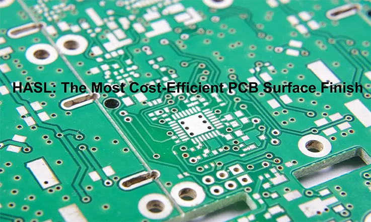
The HASL (Hot Air Solder Leveling) surface finish is a commonly used option in the manufacturing of printed circuit boards (PCBs). It involves the application of a thick layer of solder onto the copper traces of the PCB to protect them from corrosion and facilitate soldering during assembly. In this article, we will explore the advantages and disadvantages of using HASL as a surface finish from the perspective of PCB manufacturers.
What Is PCB HASL Surface Finish?
PCB HASL (Hot Air Solder Leveling) is a common surface finish used in printed circuit board (PCB) manufacturing. It is a cost-effective and widely-used process that provides a protective coating and solderable surface to the copper pads on a PCB.
Advantages and Disadvantages For PCB HASL Surface Finish
It’s important to consider the specific requirements of the PCB design and the intended application when selecting a surface finish, as each option has its own advantages and disadvantages.
Advantages of PCB HASL Surface Finish:
Cost-effective: HASL is a relatively inexpensive surface finish compared to other options like ENIG or OSP, making it a cost-effective choice for certain applications.
Good solderability: HASL provides excellent solderability, making it easier to achieve good solder joints during the assembly process.
Shelf life: HASL has a long shelf life, meaning that the solderability of the PCB remains stable over an extended period, allowing for easy storage and use.
Durability: The thick layer of solder applied during the HASL process provides good protection to the underlying copper traces, making the PCB more resistant to corrosion and wear.
Disadvantages of PCB HASL Surface Finish:
Uneven surface: The leveling process of HASL can result in an uneven surface, which may not be suitable for applications where a flat and smooth surface finish is required.
Limited component spacing: The thick layer of solder applied during HASL can create challenges in close component placement, especially for fine-pitch components or high-density designs.
Not suitable for small features: HASL is not well-suited for PCBs with small solder mask openings or fine traces as the solder can bridge or create solder balls in these areas, leading to potential shorts or electrical issues.
Environmental concerns: Traditional HASL contains lead, which is a hazardous substance. While lead-free HASL is available, environmental regulations and customer preferences have pushed for the use of alternative surface finishes that are more eco-friendly.
Overall, HASL can be a suitable surface finish for certain applications, especially those that prioritize cost-effectiveness and ease of soldering. However, it may not be the best choice for PCBs with stringent requirements for surface flatness, fine-pitch components, or environmental compliance.
HASL Surface Finish Process and Equipment
The HASL (Hot Air Solder Leveling) process involves applying a layer of solder alloy onto the copper pads of a PCB and then leveling the solder using hot air. Here is an overview of the HASL process and the equipment used:
1. Flux Application: Before the solder is applied, a flux is typically applied to the PCB’s copper surface. The flux helps remove oxidation and contaminants, promoting good solder wetting and adhesion.
2. Preheating: The PCB is preheated to a specific temperature to ensure uniform solder coating and prevent thermal shock during the solder leveling process. Preheating also helps remove moisture from the PCB, which can affect solderability.
3. Solder Application: The PCB is then passed through a molten solder bath or wave, where the solder alloy is applied to the copper pads. The solder alloy is typically a tin-lead or lead-free composition, depending on the specific HASL type.
4. Solder Leveling: After the solder is applied, the excess solder is removed by passing the PCB through a hot air leveling chamber. The hot air blows over the PCB, leveling the solder and creating a smooth and flat surface finish. The temperature and airflow are carefully controlled to ensure proper leveling without causing damage to the PCB or components.
5.Cooling and Cleaning: After the solder leveling process, the PCB is cooled to solidify the solder. Any residual flux or contaminants are then cleaned off the PCB using a cleaning process, such as a water rinse or solvent cleaning, to ensure a clean and reliable surface finish.
Upon completion of the process, it is imperative to effectively remove any surplus solder and achieve a level surface by subjecting the printed circuit board to the hot air knife treatment. It is crucial to ensure proper coverage of the printed circuit boards during this step, as any exposure can lead to oxidation and deterioration of the copper, rendering the circuit board nonfunctional.
Equipment used in the HASL process typically includes:
1. Solder Bath or Wave: A tank or reservoir containing the molten solder alloy, where the PCB is passed through for solder application.
2. Hot Air Leveling Chamber: A chamber equipped with hot air nozzles or jets that blow hot air over the PCB to level the solder.
3. Preheating Oven: An oven or conveyor system used to preheat the PCB to the appropriate temperature before solder application.
4. Cooling System:A cooling mechanism, such as a conveyor or cooling fans, used to rapidly cool the PCB after solder leveling.
5. Cleaning Equipment: Equipment for cleaning the PCB after the HASL process, which may include water rinse systems, ultrasonic cleaning tanks, or solvent cleaning stations.
It’s important to note that specific equipment and process parameters may vary depending on the PCB manufacturer and the specific HASL type being used, such as traditional HASL or lead-free HASL.
HASL vs Lead-Free HASL
The HASL (Hot Air Solder Leveling) finish commonly incorporates a solder alloy consisting of lead and tin, posing potential risks to both human health and the environment. In contrast, lead-free HASL employs solder alloys that do not contain lead, rendering it more environmentally friendly and less hazardous, aligning with the current industry trends.
It is worth noting that lead has a higher melting point compared to tin, resulting in lead-free HASL having a higher melting point than traditional HASL, which utilizes lead as one of its constituent materials. Consequently, PCBs treated with lead-free HASL exhibit a matte surface finish, while HASL-treated PCBs typically display a bright finish.
In terms of mechanical strength, both HASL and lead-free HASL treatments can provide comparable results for PCBs. However, it is important to highlight that lead-free HASL contains less than 0.5% lead, whereas conventional HASL typically contains 37% lead.
| / | HASL | LF HASL |
| Lead Content | Tin and lead (37% of lead) | Tin (lead less than 0.5%) |
| Pad Performance | Glossy | Dim |
| Solderability | Good | Medium |
| Reflow soldering temperatures | 210℃ to 245℃ | 240℃ to 270℃ |
| Wave soldering temperatures | About 250℃ | About 260℃ |
Although the inclusion of lead in the solder alloy can facilitate the handling of tin wire during the soldering process, satisfactory results can still be achieved using lead-free wire through the implementation of appropriate handling techniques.
HASL vs. Other Surface Finishes
HASL (Hot Air Solder Leveling) is one of several surface finish options available for PCBs. Here is a comparison of HASL with some other commonly used surface finishes:
1. HASL vs. ENIG (Electroless Nickel Immersion Gold):
Solderability: Both HASL and ENIG offer good solderability, but ENIG provides a more even and consistent surface for soldering due to the gold layer. ENIG is especially suitable for fine-pitch components.
Flatness: ENIG provides a flat and smooth surface finish, whereas HASL may result in an uneven surface due to the leveling process.
Shelf Life: ENIG has a longer shelf life compared to HASL, as the gold layer protects the underlying nickel from oxidation.
Cost: HASL is generally a more cost-effective option compared to ENIG, which involves additional steps and more expensive materials.
2. HASL vs. OSP (Organic Solderability Preservative):
Solderability: Both HASL and OSP provide good solderability, but OSP is more suitable for applications with fine-pitch components and small solder mask openings due to its thin and even coating.
Flatness: OSP provides a flat and smooth surface finish, whereas HASL may have some unevenness due to the leveling process.
Shelf Life: OSP has a shorter shelf life compared to HASL, as the organic layer can degrade over time and with exposure to environmental conditions.
Cost: OSP is generally a more cost-effective option compared to HASL, as it requires fewer steps and materials.
3. HASL vs. Immersion Silver:
Solderability: Both HASL and immersion silver offer good solderability, but HASL is generally more forgiving in terms of solder joint reliability.
Flatness: Immersion silver provides a flat and smooth surface finish, comparable to ENIG and OSP, whereas HASL may have some unevenness due to the leveling process.
Shelf Life: Immersion silver has a shorter shelf life compared to HASL, as silver can tarnish over time.
Cost: HASL is generally a more cost-effective option compared to immersion silver, as it requires fewer steps and materials.
When selecting a surface finish, it is important to consider the specific requirements of the PCB application, such as component spacing, solderability, shelf life, flatness, and cost. Each surface finish has its advantages and disadvantages, and the choice will depend on the specific needs and priorities of the project.
PCB Design Guidelines for HASL
Here are some PCB design guidelines to consider when using HASL (Hot Air Solder Leveling) surface finish:
1. Copper Pad Design:
●Ensure that copper pads are large enough to accommodate the HASL process, typically at least 0.020″ (0.5mm) larger than the component lead size.
●Avoid irregular or non-uniform pad shapes that may cause solder bridging or insufficient solder coverage.
2. Solder Mask:
●Apply solder mask over all areas where solder is not desired to prevent solder bridging or short circuits.
●Leave exposed copper pads for component soldering.
3. Component Placement:
●Place components at an appropriate distance from each other to avoid solder bridging during the HASL process.
●Keep components away from the board edges to prevent damage during handling and ensure uniform solder coverage.
4. Silkscreen Markings:
●Ensure that silkscreen markings do not cover or overlap with solder pads.
●Clearly label polarity markings and component identifiers near the component pads.
5. Vias and Holes:
●Avoid placing vias or through-holes near solder pads, as they may interfere with the HASL process or create solder voids.
●If necessary, tent or plug vias to prevent solder wicking during the HASL process.
6. Copper Weight and Traces:
●Consider the copper weight and trace widths when designing for HASL, as thicker copper or narrow traces may impact the solderability and solder coverage.
●Optimal copper weight for HASL is typically 1 oz (35μm) or higher.
7. Panelization:
●If using panelization, ensure proper spacing between boards to allow for the HASL process without solder bridging.
●Add breakaway tabs or mouse bites to facilitate board separation after the HASL process.
8. Thermal Considerations:
●Account for the additional heat exposure during the HASL process when designing for thermal-sensitive components.
●Consider using thermal relief pads for components with large ground or power connections to facilitate solder flow.
9. Inspection and Quality Control:
●Perform visual inspections after the HASL process to check for defects such as solder bridging, insufficient solder coverage, or solder mask damage.
●Conduct electrical testing to ensure proper solder joint integrity and continuity.
Remember, these guidelines are specific to HASL surface finish and may vary depending on your specific application or manufacturer requirements. It’s always recommended to consult with your PCB manufacturer for their specific design guidelines and recommendations.
In Conclusion
The HASL surface finish offers several advantages for PCB manufacturers, including its cost-effectiveness, good solderability, durability, and long shelf life. However, it also has some drawbacks, such as an uneven surface, limited component spacing, challenges with small features, and environmental concerns.
PCB manufacturers need to carefully consider the specific requirements of their applications when choosing the appropriate surface finish, weighing the benefits and limitations of HASL against other options such as ENIG, OSP, and immersion silver. By understanding the advantages and disadvantages of different surface finishes, manufacturers can make informed decisions to ensure the optimal performance and reliability of their PCBs.

