
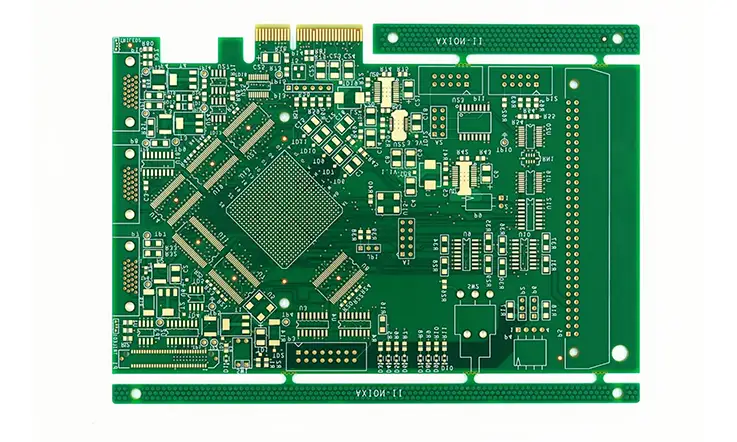
Introduction: Progressing Beyond FR-4 to Address High-Speed Design Imperatives
As data speeds increase and devices shrink, standard FR-4 substrates often limit system performance. For engineers building advanced networking, server, RF, and high-performance computing systems, PCB laminate selection has become a core engineering decision. Mid-loss materials like ITEQ IT-168G1 provide clear advantages in high-frequency designs.
However, using high-performance materials alone does not ensure project success. Moving from schematic to high-yield production demands advanced, tightly controlled fabrication practices that go beyond generic FR-4 workflows. Fully leveraging IT-168G1 requires understanding its unique properties and applying disciplined process control throughout manufacturing.
This guide provides a detailed technical overview of IT-168G1 in PCB manufacturing, focusing on its electrical and thermal strengths while outlining advanced fabrication, DFM, controlled impedance, HDI structures, and thermal management practices used at Jarnistech to turn complex high-frequency designs into reliable, high-performance boards.
The Core Merits of the ITEQ IT-168G1 Material System
Before examining the intricacies of fabrication, it is beneficial to understand why ITEQ IT-168G1 stands as a preferable option for a wide array of demanding applications. It occupies a strategic position by offering a substantial performance enhancement over conventional materials, while circumventing the prohibitive costs and processing complexities associated with specialized RF/microwave laminates.
Electrical Performance Attributes: Constructed for Signal Integrity
The principal motivation for selecting IT-168G1 is its capacity to maintain the quality of high-speed signals during their transit across the PCB.
●Stable Dielectric Constant (Dk): IT-168G1 exhibits a stable dielectric constant, nominally 3.9 at 10 GHz. In contrast to standard FR-4, whose Dk value can drift noticeably with frequency, IT-168G1 provides a predictable dielectric environment. This stability is the foundation for achieving accurate and repeatable controlled impedance, a mandatory requirement for interfaces such as PCIe, DDR, Ethernet, and SerDes.
●Low Dissipation Factor (Df): With a dissipation factor of approximately 0.008 at 10 GHz, IT-168G1 markedly reduces dielectric loss. In practical terms, this signifies that less signal energy is converted to heat as it propagates through the laminate. This low-loss profile permits longer trace lengths, accommodates higher data rates, and contributes to clean, open signal “eye” diagrams in high-speed digital systems.
●High-Frequency Suitability: The combination of a stable Dk and low Df makes IT-168G1 a highly cost-effective selection for applications extending well into the multi-gigahertz range, affording the necessary performance margin for current designs and future system upgrades.
Table: Electrical Performance Metrics of ITEQ IT-168G1
| Parameter | Value at 10 GHz | Benefit in PCB Builds |
| Dielectric Constant (Dk) | ~3.9 | Predictable impedance for high-speed signals |
| Dissipation Factor (Df) | ~0.008 | Reduced dielectric loss for longer trace lengths |
| Frequency Capability | Multi-GHz range | Supports PCIe, DDR, SerDes, and high-speed Ethernet |
Exceptional Thermal Reliability: Withstanding Lead-Free Assembly Conditions
The industry-wide shift to lead-free soldering processes introduced higher peak reflow temperatures, imposing considerable thermal stress on PCBs. The formulation of IT-168G1 is specifically engineered to endure these demanding conditions.
●High Decomposition Temperature (Td): A Td in excess of 340°C provides a substantial safety margin against thermal decomposition during multiple high-temperature assembly and rework cycles. This ensures the chemical integrity of the resin system is preserved.
●High Glass Transition Temperature (Tg): A Tg of approximately 150°C indicates the material remains rigid and dimensionally stable at elevated operating temperatures and during assembly. This behavior prevents board warpage and ensures precise component alignment.
●CAF Resistance: IT-168G1 displays a high resistance to Conductive Anodic Filament (CAF) formation. This attribute ensures long-term reliability against internal short circuits, a requirement for products deployed in humid or harsh operating environments, with performance meeting or exceeding IPC-TM-650 test methods.
Table: Thermal Reliability Metrics of ITEQ IT-168G1
| Parameter | Value | Performance Impact |
| Decomposition Temperature (Td) | >340°C | Stability during multiple reflow cycles |
| Glass Transition Temperature | ~150°C | Dimensional stability during assembly and operation |
| CAF Resistance | High (per IPC-TM-650) | Long-term reliability in humid environments |
Robust Mechanical Properties: Ensuring Long-Term Durability
The reliability of a PCB is also a function of its mechanical stability, particularly its response to thermal excursions.
●Low Z-Axis CTE: The Coefficient of Thermal Expansion (CTE) in the Z-axis (through the board’s thickness) is a determinative parameter. IT-168G1’s low Z-axis CTE (approx. 2.8% total expansion up to 288°C) minimizes the mechanical stress exerted on plated through-holes (PTHs) and vias during thermal cycling. This characteristic directly reduces the probability of barrel cracking or pad lifting, one of the most prevalent long-term failure modes in multilayer boards.
●Dimensional Stability: The material’s inherent rigidity, combined with refined fabrication workflows, ensures excellent layer-to-layer registration accuracy. This is an indispensable attribute for the successful realization of complex, high-layer-count, and HDI designs.
Table: Mechanical Properties of ITEQ IT-168G1
| Parameter | Value | Impact on PCB Performance |
| Z-Axis CTE | ~2.8% up to 288°C | Reduced PTH/via stress, minimizing cracking risks |
| Dimensional Stability | High | Accurate layer registration in HDI/multilayer builds |
The Evolution of IT-168G1 from Laminate to High-Performance Circuitry
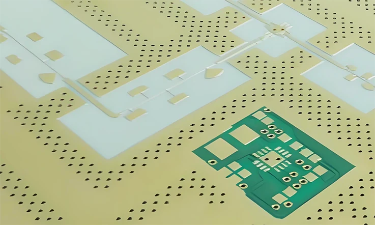
Possessing IT-168G1 raw material is one aspect; having the process expertise to fabricate it flawlessly is another. At Jarnistech, every step is optimized for this specific material system to ensure its theoretical benefits are fully realized in the final product.
Precision Lamination: The Cornerstone of Multilayer Board Construction
The lamination cycle, which fuses individual copper-clad cores and layers of prepreg into a monolithic structure, fundamentally dictates the PCB’s structural and electrical integrity.
●Environmentally Controlled Storage: All IT-168G1 laminates and prepregs are stored in an environment with strictly regulated temperature and humidity. This measure mitigates moisture absorption, a primary instigator of delamination and voids during the pressing stage.
●Verified Baking Cycles: Prior to lamination, inner layers undergo a proprietary, validated baking process to expel any residual moisture. This step is a prerequisite for preventing outgassing during the high-temperature press cycle, which can compromise layer adhesion.
●Vacuum Lamination: All high-layer-count and high-density circuit boards undergo lamination within a vacuum press. This process evacuates trapped air from between the layers before the application of heat and pressure. The result is a void-free bond, complete resin flow for uniform dielectric thickness, and superior layer-to-layer adhesion.
●Tailored Press Profiles: A “one-size-fits-all” approach is not employed. The temperature ramp rates, pressure application schedules, and cure times are precisely configured based on the specific IT-168G1 resin system, the board’s total thickness, and its unique layer stack-up. This achieves optimal resin cross-linking and minimizes internal stresses.
●Sequential Lamination: The inherent robustness of IT-168G1 makes it well-suited for complex HDI designs that demand multiple sequential lamination cycles. Advanced registration systems maintain precise layer-to-layer alignment (typically better than ±25 µm) through each successive lamination stage, a necessity for constructing reliable stacked microvia structures.
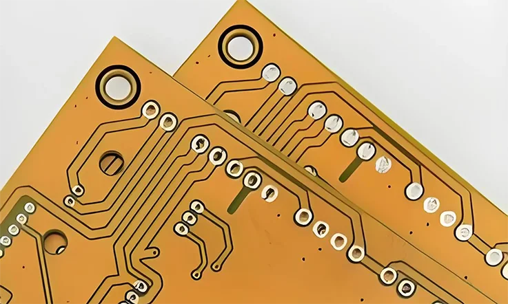
Advanced Drilling Technologies: From Microvias to Backdrilling
Vias serve as the vertical interconnects in a multilayer PCB. Their quality is a direct indicator of a facility’s technological proficiency.
●Laser Drilling for Microvias: For HDI structures, both UV (355 nm) and CO2 (10.6 µm) lasers are utilized. UV lasers are preferred for creating the smallest features on advanced dielectrics like IT-168G1, as their photochemical ablation process yields clean, sharp holes with a minimal heat-affected zone (HAZ). Process controls precisely manage beam power, pulse count, and positioning to obtain consistent via diameter and depth.
●Mechanical Drilling Optimization: For through-holes, drilling parameters—including feed rate, spindle speed, and bit geometry—are meticulously optimized for the glass/resin composition of IT-168G1. This ensures a clean-cut hole wall, free of resin smear, fiber protrusion, or fracturing, which is foundational for strong subsequent plating adhesion.
●Controlled-Depth Drilling (Backdrilling): For the most demanding high-speed applications, a backdrilling service is offered. This is a secondary, high-precision drilling operation that removes the unused, signal-distorting “stub” of a via. This process is instrumental for channels operating above 10-25 Gbps to eliminate resonant signal loss and improve overall channel performance.
Application Scenario: 400G Optical Transceiver Module
In a 400G optical transceiver design, maintaining signal integrity for the 56 Gbps PAM4 lanes across a 16-layer board is paramount. The via stubs remaining from standard through-holes act as resonant antennas, becoming a primary source of reflection and bit errors. The application of controlled-depth drilling to these specific high-speed nets removes the resonant stub structure. This action can improve insertion loss by as much as 2dB at 28 GHz, directly contributing to an open data eye and an improvement in the Bit Error Rate (BER) from a marginal 1E-9 to a robust 1E-12, enabling the design to pass stringent compliance testing.
Plating and Metallization: Ensuring Reliable Electrical Interconnection
A perfectly drilled hole without a flawless conductive plating serves no purpose. The plating processes employed are engineered for maximum reliability and uniformity.
●Advanced Hole-Wall Preparation: Following drilling, panels undergo a meticulous hole-wall preparation sequence. This includes a controlled desmear step, using either plasma or a chemical permanganate process, to remove any resin smear from the inner layer copper pads. This action creates a pristine, micro-roughened surface for superior adhesion of the plated copper.
●High-Throwing-Power Electroplating: Automated electroplating lines utilize advanced chemical formulations with high “throwing power.” This property ensures a uniform thickness of copper is deposited deep inside high-aspect-ratio holes (the ratio of board thickness to hole diameter). Uniform plating is a determinant for withstanding the mechanical stresses of thermal cycling and for carrying specified currents without creating localized hot spots.
●Continuous Process Monitoring: Plating bath chemistries are monitored in real-time, and plating thickness on test coupons from every panel is verified using X-ray fluorescence (XRF) measurements.
Section Takeaways: Core Fabrication:
1.Process Control is Foundational: The electrical and mechanical integrity of an IT-168G1 board is established through rigorous control over lamination variables, including pre-bake cycles, vacuum pressing, and tailored thermal profiles.
2.Drilling is a Precision Science: The appropriate drilling technology—optimized mechanical, laser, or high-precision backdrilling—must be matched to the design’s specific interconnect requirements to ensure both structural integrity and high-speed performance.
3.Plating Quality Determines Reliability: A reliable vertical interconnect depends on meticulous hole-wall preparation and a plating process that achieves uniform copper thickness, even in high-aspect-ratio vias, meeting IPC-6012 Class 2 or 3 requirements.
Advanced Stack-up Design and Material Integration
The architecture of the PCB stack-up itself is a field of engineering that offers significant performance and cost optimization opportunities. A high-capability facility provides not just fabrication, but also consultative guidance on advanced stack-up strategies.
Hybrid Stack-up Construction
For certain applications, the most effective solution involves integrating different types of materials within a single PCB stack-up. This hybrid approach allows for performance optimization in specific regions of the board while managing overall cost.
RF/Digital Integration:
A common example is the combination of specialized RF laminates (e.g., from Rogers or Taconic) with IT-168G1. The low-loss RF material might be used for the outer layers to support antenna elements or microwave circuits, while the more cost-effective IT-168G1 forms the core and inner layers for the digital processing sections.
Application Scenario: 5G mmWave Antenna-in-Package (AiP)
An AiP module for 5G applications requires an antenna array on the outer layers that operates efficiently at 28 GHz, demanding a very low-loss RF laminate. The underlying digital control and baseband processing circuitry, however, can be implemented on a more standard high-speed material. A hybrid stack-up using a Rogers or Taconic material for the outer RF layers and IT-168G1 for the digital core provides a cost-effective solution without compromising the performance of the critical RF section. Executing this demands mastery of disparate lamination profiles and hole-wall preparation techniques (e.g., plasma treatment for the RF layers).
Fabrication Complexities:
Executing a hybrid build presents considerable manufacturing challenges. Different materials exhibit different Coefficients of Thermal Expansion (CTE), requiring a lamination profile that carefully balances the stresses to prevent warpage. Hole-wall preparation becomes more complex; for instance, PTFE-based RF materials are chemically inert and mandate a plasma treatment process to activate the hole wall surface for proper plating adhesion, a step not required for the epoxy-based IT-168G1 layers. Managing these disparate process requirements within a single build demands a high degree of process engineering expertise.
Understanding Glass Styles and Resin Content
Going beyond the material’s datasheet name, a deeper understanding of its composition allows for fine-tuning performance. The fiberglass weave style and the resin-to-glass ratio in the prepreg are selectable variables.
Glass Weave Styles:
Laminates are offered with various glass cloth styles (e.g., 106, 1080, 2116, 3313), with these numbers reflecting different weave densities and thicknesses. Looser weaves like 1080 feature larger openings in the glass fabric, which can introduce localized shifts in the dielectric constant when routing very fine traces. In contrast, tighter and flatter weaves, often referred to as “spread glass,” create a more uniform dielectric environment that helps reduce the fiber weave effect, supporting stable impedance behavior across high-frequency signals.
Resin Content (RC):
Prepregs can be specified with different resin contents. High RC prepregs are better at filling large copper-free areas and encapsulating heavy copper features. Low RC prepregs result in thinner dielectric layers, which can be useful for creating low-impedance power distribution networks. However, selecting the appropriate RC is a balance; an incorrect choice can lead to issues like incomplete filling of voids or resin starvation. An experienced engineering team can guide the selection of the optimal glass style and resin content based on the specific design’s geometry and performance targets.
HDI Technology: Maximizing Density and Performance in Limited Space
Modern electronics mandate unprecedented routing density. HDI technology is the methodology for achieving compact, high-performance designs, and the ability to implement it flawlessly on materials like IT-168G1 is a defining attribute of a top-tier fabrication facility.
Microvias: The Building Blocks of HDI
Microvias are laser-drilled, small-diameter holes (typically < 150 µm) that connect adjacent layers. They are the fundamental elements of HDI construction.
●Increased Routing Density: By replacing space-consuming through-hole vias, microvias dramatically increase the usable routing area on each layer. This enables the use of fine-pitch components (e.g., 0.4 mm BGAs) and can often reduce the total layer count of a board, yielding cost benefits.
●Improved Signal Integrity: Due to their diminutive size, microvias exhibit significantly lower parasitic capacitance and inductance compared to standard vias. This translates to reduced signal distortion, lower crosstalk, and a cleaner propagation path for high-frequency signals.
●Stacked vs. Staggered Microvias: Both stacked and staggered microvia configurations are supported.
●Stacked Microvias: These are constructed directly atop one another across multiple layers, offering the most direct Z-axis interconnect. This requires a highly controlled process of filling each microvia with conductive material and planarizing its surface before the subsequent layer is added.
●Staggered Microvias: These are offset from each other on adjacent layers. While slightly less space-efficient, this configuration is often more robust from a fabrication standpoint. Engineering staff can collaborate with designers to select the optimal approach based on density requirements and reliability targets.
Table: Microvia HDI Process Metrics:
| Attribute | Value/Detail | Practical Impact |
| Microvia Diameter | <150 µm | Enables fine-pitch BGA routing |
| Microvia Depth Capability | 1:1 aspect ratio (typical) | Reliable interlayer connectivity |
| Stacked Microvia Layers | Up to 4 layers stackable | Direct Z-axis routing for dense designs |
| Staggered Microvia Layers | Multiple configurations supported | Enhanced mechanical robustness |
| Aspect Ratio Control | Maintained during laser drilling and filling | Prevents voids and ensures electrical continuity |
Via-in-Pad Plated Over (VIPPO): Optimizing Routing and Signal Paths
VIPPO is an advanced technique wherein the microvia is placed directly within the solder pad of a surface-mount component and subsequently plated over with copper to create a flat, solderable surface.
●Shortest Possible Signal Path: VIPPO provides the most direct connection from the component to the inner layers, minimizing via inductance and substantially improving signal integrity for high-speed signals.
●Enhanced Routing Space: It obviates the need for traditional “dog bone” via transitions, freeing up routing channels directly beneath dense components like BGAs. This is often the sole method for successfully escaping all signals from a high-pin-count device.
●Improved Thermal Management: Placing thermal vias directly in the thermal pads of components using the VIPPO process creates a highly efficient heat conduction path away from the component die.
Application Scenario: Compact AI Accelerator Module
An AI accelerator module features a high-power System-on-Chip (SoC) in a fine-pitch BGA package. The design is severely space-constrained, requiring power and signal lines to be routed directly under the component. The VIPPO process allows for placing microvias directly in the BGA pads for signal escape, freeing up all available channels for routing. Simultaneously, applying VIPPO to the thermal pads creates a dense array of filled thermal vias, providing a low-resistance path to conduct heat away from the SoC, ensuring its thermal stability under heavy computational loads and achieving a 15°C reduction in die temperature compared to standard thermal designs.
●Manufacturing Execution: Flawless execution of VIPPO demands exceptional control over the via filling process (to prevent dimples or voids) and planarization techniques to ensure a perfectly flat surface for reliable solder joint formation.
Blind and Buried Vias: The Art of Complex Multilayer Routing
For the most intricate, high-layer-count designs, blind and buried vias are indispensable routing tools.
●Blind Vias: These connect an outer layer of the PCB to one or more inner layers without traversing the entire board. They are instrumental for escaping signals from dense BGAs on one side of the board while preserving uninterrupted ground planes or routing channels on the opposite side.
●Buried Vias: These connect only two or more inner layers and are completely sealed within the board’s structure. They are the workhorses of complex designs, permitting dense sub-routing (e.g., between power and ground planes, or within specific signal groups) without consuming any space on the valuable outer layers.
●Sequential Build-Up (SBU) Process: The creation of these structures necessitates a multi-stage SBU process. Subsets of layers are fabricated as independent “cores,” which are drilled, plated, and imaged before being laminated together in subsequent cycles. This complex, multi-stage workflow demands exceptional layer-to-layer registration accuracy and process control.
Section Takeaways: High-Density Interconnect (HDI):
1.HDI Unlocks Density: Microvias, blind vias, and buried vias are the tools that enable complex routing in compact designs, allowing for the use of fine-pitch components and often reducing board layer count and cost.
2.VIPPO Maximizes Performance: Placing vias directly in solder pads (VIPPO) offers the shortest possible signal and thermal paths, simultaneously improving signal integrity, thermal dissipation, and routing density.
3.Execution Demands Expertise: HDI fabrication, especially with stacked microvias and multiple sequential laminations, is a complex process that requires exceptional precision in laser drilling, filling, planarization, and layer-to-layer alignment.
Signal Integrity Engineering: Precision Controlled Impedance and Channel Performance
For any high-speed digital or RF circuit, maintaining a specified characteristic impedance along a signal’s path is not an optional feature but a fundamental operational requirement. The approach to achieving this is a disciplined, multi-phase process that ensures performance from simulation to physical realization.
Phase 1: Collaborative Modeling and Simulation
Success originates before the first piece of copper is etched. A collaborative engagement with client design teams helps to construct a manufacturable digital twin of the stack-up.
●Collaborative Stack-up Design: Utilizing industry-standard field-solving software (e.g., Polar Instruments), engineers input the client’s design targets (e.g., 50Ω single-ended, 90Ω differential) and the known electrical properties of IT-168G1 at the specified operating frequencies.
●Generating Precise Geometries: The field solver calculates the exact physical geometries—trace width (W), trace thickness (T), and spacing between differential pairs (S)—required for each signal layer to achieve the target impedance. The process accounts for the differing electromagnetic field configurations of outer-layer microstrip and inner-layer stripline traces.
●Manufacturing Compensation: The model incorporates specific fabrication process variables. It accounts for the slight reduction in trace width during the etch process (undercut) and the final pressed thickness of the prepreg material. The imaging artwork is pre-compensated to ensure the final physical board dimensions align with the theoretical model’s requirements.
Table: Modeling and Simulation Parameters
| Parameter | Typical Value/Approach |
| Target Impedance | 50Ω (SE), 90Ω (Diff) |
| Trace Width (W) | Calculated per stack-up, adjusted for etch |
| Trace Thickness (T) | Copper thickness as plated/etched |
| Differential Pair Spacing (S) | Calculated per target impedance |
| Dielectric Constant (Dk) | IT-168G1: 3.9 @ 10GHz |
Phase 2: Precision Control in Manufacturing
A perfect model holds no value if the fabrication process cannot replicate it with high fidelity.
●Dielectric Height (H) Control: The distance from a trace to its reference plane(s) is a direct factor in the impedance calculation. A tightly controlled lamination process ensures a consistent pressed dielectric thickness across the entire panel, minimizing impedance deviations.
●Trace Width (W) Control: Laser Direct Imaging (LDI) is employed for all critical layers, providing higher accuracy than traditional film methods and eliminating phototool-related distortions. The chemical etching processes are continuously monitored and calibrated to control the amount of undercut, ensuring the final average trace width is within a tight tolerance (typically ±5% for impedance-controlled traces) of the design specification.
Phase 3: Empirical Proof with Time Domain Reflectometry (TDR)
The final phase is to empirically verify that the manufactured board meets the impedance specification. This is accomplished through TDR testing on a test coupon fabricated on every production panel.
●The TDR Principle: A TDR instrument propagates a very fast rise-time pulse down a specially designed test trace on the coupon and monitors for reflections. Any deviation in impedance—caused by a variation in trace width, dielectric height, or spacing—will generate a reflection.
●Data Interpretation: The TDR displays a plot of impedance (in Ohms) versus electrical distance along the trace. A passing result is a flat line centered on the target impedance within the specified tolerance (e.g., 50Ω ± 5Ω).
●Verification and Assurance: The TDR report provides objective, graphical proof that the manufacturing process controls have successfully translated the theoretical model into a physical reality. These reports are archived for process control and can be supplied as definitive evidence of compliance and quality.
Table: TDR Testing Metrics
| Attribute | Value / Method | Application |
| Measurement Method | Time Domain Reflectometry (TDR) | Validates impedance on each production panel |
| Typical Tolerance | ±5Ω around target (e.g., 50Ω ± 5Ω) | Confirms process precision |
| Test Coupon Design | Mirrors customer stack-up with matching geometry | Ensures test accuracy reflecting real conditions |
| Data Output | Impedance vs. electrical distance plot | Visual confirmation of compliance |
| Archive and Traceability | TDR reports archived for each batch | Enables quality audits and traceability |
Advanced Channel Performance Considerations: Crosstalk and Skew
Beyond single-trace impedance, overall channel performance depends on managing interactions between traces.
●Crosstalk Mitigation: Crosstalk, the unintended coupling of energy between adjacent traces, can corrupt signals. Its mitigation involves layout discipline. DFM reviews analyze trace-to-trace spacing against specified rules. For high-density designs, routing critical pairs as striplines (sandwiched between ground planes) offers superior shielding and lower crosstalk compared to microstrip routing. The use of guard traces, grounded traces run parallel to sensitive nets, can further isolate signals.
Application Scenario: Dense DDR4 Memory Interface
On a motherboard with a dense DDR4 memory interface, the address and data busses are tightly packed. Unmanaged crosstalk between adjacent traces can reduce noise margins and cause data bit errors. DFM analysis flags areas where trace spacing is below recommended guidelines. The solution involves a combination of increasing spacing where possible and strategically routing the most sensitive nets on inner stripline layers. This use of stripline routing can reduce far-end crosstalk (FEXT) by more than 10dB compared to an equivalent microstrip layout, ensuring reliable memory operation at maximum data rates.
●Skew Management: Skew refers to the time-of-arrival difference between signals that are intended to arrive simultaneously.
1.Intra-pair skew: This occurs within a differential pair when the two traces have different physical lengths. It is corrected by adding small, serpentine length-tuning patterns to the shorter trace, typically keeping lengths matched to within 1.25mm.
2.Inter-pair skew: This occurs between different signal groups, such as between a clock line and its associated data bus. It is managed by meticulous length matching of all related nets across the entire bus. Engineering review processes verify that these length-matching rules are met to ensure proper data timing at the receiver.
Section Takeaways: Signal Integrity Engineering:
1.Impedance is a Three-Part Discipline: Achieving accurate controlled impedance is a process of collaborative modeling, precision manufacturing control, and empirical verification with TDR.
2.Models Must Reflect Reality: The most accurate impedance models are those that pre-compensate for the specific, known variables of the fabrication process, such as etch factor and pressed dielectric thickness.
3.Channel Performance Extends Beyond Impedance: Managing crosstalk through strategic routing and controlling skew through meticulous length matching are equally fundamental for the successful operation of high-speed parallel and serial interfaces.
Table: Advanced Channel Performance Metrics
| Attribute | Target / Method | Outcome |
| Crosstalk Reduction Target | >10dB FEXT improvement using stripline vs. microstrip | Ensures data integrity in dense interfaces |
| Intra-pair Skew Control | Length matching within ±1.25mm | Preserves differential pair timing |
| Inter-pair Skew Control | Length matching across related signals | Maintains bus timing for high-speed systems |
| Guard Trace Utilization | Placed adjacent to sensitive signals, grounded | Further reduces crosstalk and interference |
| DFM Review Focus | Trace spacing and layer selection | Prevents performance degradation pre-fabrication |
Surface Finish Selection: The Final Interface for High-Frequency Applications
The surface finish is the final coating applied to the copper pads of a PCB. It serves to protect the copper from oxidation and provide a solderable surface for component assembly. For high-frequency designs using IT-168G1, the finish selection directly impacts both performance and assembly reliability.
Electroless Nickel Immersion Gold (ENIG)
ENIG is a very common finish for high-performance applications due to its excellent balance of properties.
●Process: It involves the deposition of an electroless nickel layer onto the copper, followed by a thin layer of immersion gold.
Attributes:
1.Flat Surface: Provides a perfectly flat (coplanar) surface, which is a prerequisite for reliable soldering of fine-pitch components like BGAs and QFNs.
2.Excellent Solderability: The gold layer protects the underlying nickel from oxidation, ensuring robust solderability even after extended storage.
●High-Frequency Considerations: At very high frequencies (e.g., >10-15 GHz), the “skin effect” causes a portion of the signal current to travel through the more resistive nickel layer, which can slightly increase the overall insertion loss of the channel. This is a design trade-off that engineering staff can help to evaluate.
Electroless Nickel Electroless Palladium Immersion Gold (ENEPIG)
ENEPIG adds a layer of palladium between the nickel and the gold, earning it the designation of a “universal finish.”
●Process: The deposition sequence is Copper -> Nickel -> Palladium -> Gold.
Attributes:
1.Prevents “Black Pad”: The palladium layer acts as a diffusion barrier, preventing the nickel from migrating into and reacting with the gold layer. This reaction can create a brittle, unreliable solder joint (a phenomenon known as “black pad”). The use of ENEPIG significantly enhances long-term solder joint reliability.
2.Gold Wire Bondable: ENEPIG provides an excellent surface for both soldering and gold wire bonding, making it suitable for complex hybrid assemblies that incorporate bare die.
3.Superior Performance: It mitigates the high-frequency insertion loss concerns associated with ENIG and offers the highest level of reliability for mission-demanding or aerospace applications.
Immersion Silver (ImAg) and Organic Solderability Preservative (OSP)
These finishes are also available and have specific use cases.
●Immersion Silver: Offers excellent electrical performance at high frequencies (as the signal travels on pure silver) and a very flat surface. However, it is sensitive to handling and can tarnish if exposed to atmospheric contaminants, requiring a more controlled assembly environment.
●OSP: A thin organic coating that protects the copper from oxidation. It is a very cost-effective and flat finish but has a limited shelf life and can typically only withstand one or two reflow soldering cycles. It is generally not specified for complex, high-value IT-168G1 boards.
Holistic Thermal Management Solutions: Ensuring Stability Under Load
High-performance circuits often produce considerable thermal loads. Managing this heat effectively is as basic to reliable operation as maintaining signal quality. Facilities supporting these builds need to offer the practical capabilities and layout planning support necessary to apply reliable thermal strategies.
Thermal Via Arrays
A straightforward yet highly effective technique for conducting heat away from components.
●Function: An array of plated through-holes is placed directly under or adjacent to a heat-generating component. These vias act as thermal conduits, transferring heat from the top layer of the board down to internal power or ground planes, or to a bottom-side heatsink.
●Optimization: Engineering guidance can recommend the optimal via size, plating thickness, and array pattern to maximize heat transfer without compromising signal routing integrity. A well-designed thermal via array can reduce component operating temperatures by 5-10°C under typical loads.
Heavy Copper and Embedded Coins
For applications with extreme power delivery or thermal dissipation requirements, more advanced solutions are necessary.
●Heavy Copper: The capability exists to manufacture boards with heavy copper layers (e.g., 3 oz. to 10 oz. copper or more). These thick copper planes are excellent for both carrying high currents with minimal voltage drop and for spreading heat laterally across the board, reducing hot spots.
●Embedded Coins: For the ultimate in localized heat removal, a solid copper or aluminum coin can be embedded directly into a cutout in the PCB and laminated in place. The heat-generating component is then mounted directly onto this coin, creating a direct, low-resistance thermal path to an external heatsink. This technique can achieve localized temperature reductions of 15-25°C or more, enabling performance levels unattainable with other cooling methods.
Design for Manufacturability (DFM): Collaborative Engineering to Preempt Fabrication Issues
A successful project is the result of a collaborative effort. A comprehensive DFM engineering review is a value-added service that extends beyond a simple rules check. The engineering function acts as an extension of the client’s team to proactively identify and resolve design elements that could negatively impact cost, yield, or final product reliability.
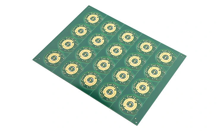
Panelization and Array Optimization: Maximizing Efficiency and Cost-Effectiveness
The arrangement of individual boards on a large production panel has a profound impact on the final unit cost.
●Material Utilization: The primary objective is to nest the client’s design onto standard 18″ x 24″ panels in a way that minimizes material waste. For irregularly shaped boards, nesting algorithms are used to interlock them, which can dramatically improve material yield and lower the per-unit cost.
●Copper Balancing: The DFM process analyzes the copper distribution on every layer of the panel. Unbalanced copper—where one area of the panel is dense with copper and another is sparse—can cause uneven stresses during the heat and pressure of lamination and assembly. This can lead to warpage that exceeds the IPC-A-600 limit of 0.75% for bow and twist, compromising the assembly process. The analysis may recommend adding non-functional copper “thieving” patterns to sparse areas to ensure a balanced, flat, and stable panel.
●Depanelization Strategy: Guidance is provided on the optimal method to separate boards from the array:
1.V-Scoring: Ideal for rectangular boards, offering maximum panel space efficiency. Advice is given on clearance requirements for components near the score line to avoid mechanical stress during separation.
2.Tab Routing: A necessity for non-rectangular boards or designs with edge-sensitive components. The placement and style of tabs (often incorporating “mouse bites”—a series of small, non-plated holes) are optimized for a clean break with minimal post-separation finishing required.
Common Design Pitfalls and Their Proactive Avoidance
Leveraging IT-168G1 requires avoiding common design traps that can negate its benefits. The DFM review flags these issues before they enter fabrication.
Pitfall 1: Discontinuous Signal Return Paths:
●Problem: Routing a high-speed signal across a split in its reference ground plane forces the return current to take a long, circuitous detour. This creates a large current loop that radiates EMI and adds significant inductance to the path, degrading the signal.
●DFM Solution: The DFM check automatically flags such violations. The governing rule is: Never cross a plane split with a high-speed trace. The review also ensures that for layer transitions, a ground-stitching via is placed immediately adjacent to the signal via to provide a short, direct path for the return current.
Pitfall 2: Neglecting Annular Ring Requirements:
●Problem: The annular ring is the ring of copper pad that remains around a drilled hole. If the pad is too small or the hole is drilled off-center, the resulting annular ring may be insufficient (or “break out” of the pad), leading to a weak or non-existent connection between the via barrel and the trace.
●DFM Solution: The review process checks that all drilled holes meet minimum annular ring requirements as specified by IPC-6012 Class 2 or Class 3. For Class 3, this mandates a minimum of 50µm (2 mils) for internal and 25µm (1 mil) for external annular rings, ensuring a robust, reliable connection.
Pitfall 3: Acid Traps:
●Problem: Acute angles (< 90 degrees) in a PCB layout can “trap” etching chemicals. The trapped etchant continues to work on the copper longer than intended, which can over-etch the trace, creating an open circuit or an impedance violation.
●DFM Solution: Automated checks identify acute angles. The recommendation is to modify all trace junctions to use 90-degree or 45-degree angles, or to apply “teardrops,” which create a smooth fillet between traces and pads, eliminating the sharp corners.
Section Takeaways: Design for Manufacturability (DFM)
1.DFM is Proactive Engineering: It is a process of identifying and correcting potential fabrication, assembly, and reliability issues in the design phase, before they result in costly delays or field failures.
2.Panelization Directly Impacts Cost: An intelligent panelization strategy that maximizes material utilization and ensures panel stability through copper balancing directly reduces the per-unit cost of the final board.
3.Avoiding Common Pitfalls Preserves Performance: Simple design oversights like return path discontinuities or insufficient annular rings can completely negate the benefits of a high-performance material. A thorough DFM review is a safeguard against these issues.
Commitment to Quality: Comprehensive Assurance and Validation
For high-reliability electronics, confidence in the final product is built upon a foundation of objective evidence. A robust quality management system is based on rigorous testing, validation, and complete material traceability.
Strict Material Traceability and Supply Chain Integrity
●Authentic Sourcing: All ITEQ IT-168G1 laminates and prepregs are procured exclusively from authorized distributors or directly from the material supplier. This practice guarantees material authenticity and prevents counterfeit or out-of-spec materials from entering the supply chain.
●Lot-to-Lot Traceability: Every panel of raw material is marked with a unique lot code. This code is scanned and tracked through every single manufacturing step—from inner-layer imaging and lamination to final inspection. This provides an unbroken chain of custody.
●Performance Repeatability: This system guarantees that a board used in a prototype run is made from the same material class as one in a high-volume build months later. This ensures performance repeatability and provides a complete manufacturing history, which can be invaluable for failure analysis or regulatory compliance.
A Protocol of In-Process and Final Validation Testing
●In-Process Quality Control (IPQC): Quality is verified at every stage. This includes 100% Automated Optical Inspection (AOI) of every internal layer before lamination to detect shorts, opens, or incorrect trace geometries, with all findings evaluated against IPC-A-600 standards.
●Microsectional Analysis: On a regular basis and for every new design, coupons are cut from production panels, mounted in epoxy, and polished to reveal a cross-section of the PCB’s internal structure. This microscopic examination verifies correct layer-to-layer registration, uniform copper plating thickness inside via barrels, the integrity of the inner-layer connections to the via, and the quality of the lamination bond.
●Final Electrical Test: Every single board undergoes a “flying probe” or “bed-of-nails” electrical test to verify the netlist. This testing is performed to the standards of IPC-9252 Class 2, ensuring there are no open circuits or short circuits.
●High Potential (Hi-Pot) Testing: For applications requiring high-voltage isolation, Hi-Pot testing can be performed. This test applies a high voltage between different conductors to stress the dielectric material. A passing result confirms the dielectric strength and the absence of any latent defects that could lead to a short circuit under high-voltage conditions.
Why Choose Jarnistech for Your ITEQ IT-1-68G1 Project?
Choosing the right supplier for a high-frequency PCB project shapes the outcome, defining whether the result meets advanced design requirements or falls short of expectations. Working with Jarnistech on an ITEQ IT-168G1 build brings a level of proven capability across all relevant technical and quality measures, ensuring that each board aligns with the precision and performance demands of high-speed, high-frequency applications.
1.Uncompromising Quality and Expertise:
The entire operation is founded on a zero-defect philosophy and adherence to the strictest IPC-A-600 Class 2 and Class 3 acceptability standards. The deep, specialized expertise in processing advanced materials like IT-168G1 signifies an understanding of the nuances that generic fabricators may miss. The objective is not just to build a board, but to ensure it is built correctly.
2.Superior Manufacturing Capability:
We facility is equipped with the state-of-the-art technology required for today’s most demanding designs: LDI, laser drilling, backdrilling, VIPPO, sequential lamination, and high-throwing-power plating. The facility possesses the tools, processes, and personnel to transform the most complex high-frequency designs into successful, reliable products.
3.Dedicated, Collaborative Engineering Support:
Clients receive access to a dedicated team of experienced DFM and Signal Integrity engineers who function as an extension of the client’s own team. Proactive feedback and a collaborative approach save time, capital, and costly design iterations.
4.Exceptional Value and Competitive Pricing:
As a leading manufacturer in China, we leverages a highly optimized supply chain and efficient manufacturing processes. This structure enables the firm to offer truly competitive pricing without ever compromising on materials, technology, or quality. The goal is to provide clients with the best possible total cost of ownership through superior execution and reduced waste.
5.Reliable, Agile, and Transparent Operations:
An understanding that time-to-market is a competitive advantage drives the operational model. Streamlined processes, from engineering review to final shipment, are designed for efficiency and transparency. Agile scheduling is offered for everything from rapid prototypes to high-volume builds, and clear communication ensures clients are always apprised of their project’s status, guaranteeing dependable, on-time delivery.
Begin Your High-Performance PCB Project with an Expert
Ready to transform your complex IT-168G1 design into a reliable, high-performance product? Take the next step with confidence. Engage with a manufacturer that possesses the expertise, technology, and commitment to ensure your project’s success from the very first board.
●Request a Detailed Quote for your upcoming project.
●Schedule a Technical Consultation with a Jarnistech engineering specialist.
●Submit Your Design Files for a complimentary, in-depth DFM review.
Discover the Jarnistech advantage today.
FAQs for ITEQ IT-168G1
Q: At GHz frequencies, how can the “Fiber Weave Effect” be mitigated during the fabrication of IT-168G1 boards?
A: By using flatter glass styles (e.g., 1078, 1080) and ensuring sufficient resin fill during lamination, in addition to rotating the routing angle during design.
Q: In multi-layer IT-168G1 designs with large copper planes, how is localized “Resin Starvation” prevented?
A: By patterning large copper areas with a grid (hatching) and using a high-flow prepreg to ensure uniform resin flow during lamination.
Q: For signals requiring back-drilling, what precision can be achieved for the remaining stub length on IT-168G1?
A: The remaining stub length can be controlled to within +/- 50µm (2 mils) through depth-controlled drilling, which is then verified by X-ray inspection.
Q: In Via-in-Pad designs, how is the risk of solder voiding reduced on IT-168G1 boards post-assembly?
A: By using a process where the via is filled with resin and then plated over with copper (capped via), creating a flat pad that prevents solder voiding during reflow.
Q: When high-power components are placed on an IT-168G1 board, what special thermal enhancements can be made during fabrication?
A: Through advanced fabrication techniques like incorporating an embedded copper coin or using heavy copper layers, both of which require specialized lamination and plating procedures.
Q: On an IT-168G1 board, how is an optimal signal “launch” from an RF connector to a microstrip trace ensured?
A: By optimizing the antipod dimensions under the connector and applying precise etch controls to the surface trace, ensuring a smooth 50-ohm impedance transition.
Q: For asymmetrical IT-168G1 stack-up designs, how is post-reflow warpage controlled?
A: Through in-panel copper balancing techniques and the use of balancing coupons during lamination to counteract the internal stresses of the design.
Q: How does the etch compensation process for IT-168G1 differ from standard FR-4?
A: It requires more precise compensation values based on the specific copper foil type and thickness, ensuring final fine-line trace widths meet tighter tolerances (e.g., ±10% or better).


