
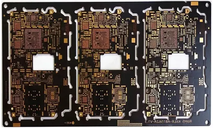
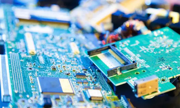
Over the past few decades, there has been a notable shift in the consumer electronics industry, as well as in other sectors, towards smaller and lighter devices that offer improved speed, performance, and efficiency. This transition is largely due to the emergence of High Density Interconnect Printed Circuit Board (HDI PCB) Layout.
HDI PCB Layout designs incorporate high-density elements such as laser microvias, fine lines, and high-performance thin materials. The benefit of these high-density features is that they offer a higher wiring density per unit space compared to conventional PCBs. This makes HDI PCBs an excellent solution for complex, compact form factor designs.
By utilizing HDI PCBs, designers can achieve greater efficiency while also maximizing space on PCBs, facilitating faster transmission, and better device functionality. In summary, High Density Interconnect PCB Layout is a key enabling technology that has driven advancements in the electronics industry and paved the way for continued progress in cutting-edge electronic devices.
What Is High Density Interconnect (HDI) PCB?
High Density Interconnect PCBs (HDI PCBs) offer a multitude of benefits in printed circuit board design, most notably the ability to downsize PCBs by packing an increased number of interconnections into a smaller space. The microvias used in an HDI PCB are typically less than .006 millimeters in diameter, which enables PCB designers to fit more functionalities into the same space while maintaining high performance standards.
Moreover, the use of blind and buried vias in HDI PCB designs significantly reduces stray capacitances and inductances, which results in improved signal integrity. This feature is particularly vital in complex electronic systems where signal transmission speed and accuracy are critical.
The ongoing development of High Density Interconnect PCB technology is driven by innovative methodologies, the increasing miniaturization of components, and advancements in semiconductor packaging. These factors support the integration of advanced features into revolutionary new products for use in various application areas such as wearable electronics, touch screen computing, compact-gadgetry, as well as in defense and aerospace.
In summary, HDI PCBs are a game-changer in the electronic industry due to their ability to enable the design of highly compact and efficient systems, making them an ideal solution for modern cutting-edge electronic devices.
Introduction to HDI PCB Layout
As PCB design engineers, we understand the term “high density interconnects” (HDI) PCB Layout, which encompasses a set of techniques utilized in PCB design with trace widths often below 8 mils(0.2mm). These techniques are employed to facilitate the integration of a higher density of components onto a single board, allowing for a small board size with a higher component count. However, not all boards require HDI layout techniques for design, as some boards may have fewer or larger components that are compatible with other PCB layout techniques.
To enable proper routing, HDI PCB layout for fine-pitch BGA components requires smaller vias for layer transition, with more traces per square millimeter. Therefore, HDI layouts will typically feature design characteristics such as the utilization of blind and buried vias, microvias, and the placement of components in closer proximity. By incorporating such specific design features, designers can ensure components with finer pitch are more effectively manageable in an HDI PCB Layout.
In summary, HDI PCB Layout is an advanced PCB design methodology that maximizes PCB space usage and component density, allowing for smaller PCB footprints without sacrificing functionality. While various factors determine whether HDI layout techniques are necessary, for complex designs with higher component counts or finer pitch components, HDI techniques are an essential solution to maximize board space utilization while ensuring excellent signal and power integrity.
In order to make room for components with a finer pitch, an HDI layout will typically include the following characteristics:
● Lower Signal Levels: HDI circuit boards are typically not suitable for managing high current flows or electrical voltages. This is attributed to the potential for electrostatic discharge (ESD) to occur due to high field strength between adjacent lines, as well as the potential for excessive temperature increases in conductors induced by large currents. It is important for PCB design engineers to consider these limitations and choose appropriate materials and techniques when designing circuit boards for high current or voltage applications.
● Higher Layer Count: While we have successfully developed printed circuit boards (PCBs) with a high number of layers in the past, HDI (High-Density Interconnect) boards are the preferred option for handling high-pin-density components like FPGAs when requiring 20 layers or more. Given the intricate design of such components and the limited space available on the board, HDI technology enables the routing of dense traces that would not be possible with traditional board designs. As such, it is crucial for PCB design engineers to consider HDI technology when developing high-density designs to ensure optimal performance and functionality.
● Thinner Traces: HDI (High-Density Interconnect) technology employs thin traces to facilitate connections with vias on every layer of the PCB, as well as in-pad vias. The use of thin traces is essential in enabling the creation of high-density circuit connections that otherwise would not be achievable with conventional PCB designs. The resulting ability to achieve significantly higher trace densities is what characterizes HDI technology. It is imperative for PCB design engineers to carefully consider the use of HDI technology when developing designs requiring complex circuit connections and high trace densities.
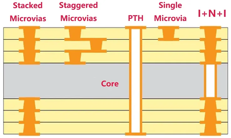
● Smaller Vias: HDI (High-Density Interconnect) PCBs utilize various via types for layer transitions, such as mechanically or laser-drilled microvias, as well as blind/buried and staggered vias. Compared to standard through-hole vias, these vias have significantly reduced aspect ratios. The smaller diameter of HDI vias allows for their use with components featuring fine pitch, although this type of via does have limitations with respect to depth capacity. As such, PCB design engineers need to carefully consider the via types to use based on the component pitch and overall design requirements when designing HDI PCBs.
In conjunction with IPC (Association Connecting Electronics Industries) standards, a PCB designer can use the factors mentioned above to determine when a board requires HDI layout and routing strategies.
The IPC-2221A/IPC-2222 specifications recommend a maximum aspect ratio of 8:1 for through-hole vias. Aspect ratio is calculated by dividing via depth by diameter. Based on the typical PCB thickness of 1.57 mm, through-hole vias should have a minimum drill diameter of 0.196 mm or around 8 mils. However, for fine-pitch components, smaller vias are necessary, which requires the adoption of HDI-specific via designs and thinner traces. It is important for PCB design engineers to consider these factors and IPC specifications to ensure optimal PCB design and performance.
Our Capabilities and Advantages of HDI PCB Layout Design
As a PCB manufacturer, JarnisTech employs a range of techniques to develop high-density interconnect layouts that are both efficient and cost-effective. Our approach includes the use of stacked and staggered vias/microvias, fine lines and spaces, blind and buried vias, sequential lamination, and via-in-pad technology.
One of the most critical advantages of HDI PCB Layout is the utilization of microvias, which are smaller and more effective in terms of space utilization than traditional vias. Although the microvia process can increase the cost of the High-Density Interconnect PCB, we can reduce both the cost per material square inch and the cost per layer count through proper design and a reduction of layers.
Our team has extensive experience in designing cost-effective HDI PCB Layouts that incorporate advanced techniques, including microvias, blind and buried vias, fine lines and spaces, sequential lamination, and via-in-pad technology. These techniques help our customers decrease the size and weight of their devices while improving their electrical performance.
At JarnisTech, our HDI PCB Layout Services include Library Management, PCB Layout and Analysis, Power Integrity Analysis Services, Signal Integrity Analysis Services, Structural Analysis Services, and Thermal Analysis Services. We are committed to providing our customers with PCB manufacturing solutions that meet their unique needs and requirements.
JarnisTech is fully equipped to cater to all your PCB manufacturing needs. With over 20 years of experience in the industry, we specialize in manufacturing and assembling PCBs of varying complexities while adhering to the highest industry standards. Our team of experts and advanced equipment ensure that all our PCBs meet the rigorous quality and testing requirements of the industry. We take pride in our extensive portfolio of satisfied clients, which serves as a testament to our achievements. Should you have any questions or inquiries, please don’t hesitate to contact us via email at [email protected].
HDI layout’s Trace Sizes and Vias
HDI designs have become essential due to the demand for fine pitch components and higher component density. Traces are created in the same manner as on any other PCB, with particular attention given to avoiding excessive etching. In cases where blind or buried vias are required, laser drilling may be necessary through a single layer, particularly for low aspect ratio vias.
In compliance with IPC requirements, through-hole vias cannot be used to span multiple layers on an HDI board, as this could potentially pose safety hazards. However, some manufacturers have the capability to produce blind vias that span multiple layers, although this is not very common and is only possible for microvias with larger diameters.
Incorporating non-compliant designs in your HDI board may result in your PCB receiving no-bid status from the manufacturer due to their DFM rules. Instead, individual layer vias can be stacked, such as with stacked microvias or blind-buried vias, to achieve the required results. These via configurations are typically used for BGA components with varying pitches.
When dealing with a BGA pitch of 0.8 millimeters or smaller, you can use a dog bone fanout in combination with in-pad microvias to achieve the desired results. When the distance between the pads is less than or equal to 0.75 mm, the preferred method for reaching inner signal layers is the use of plated in-pad microvias (VIPPO) rather than routing signals between pads. It is not advisable to route between pads when the pitch is significantly lower, such as 0.5 mm, unless your manufacturer is capable of creating traces that are smaller than 4 mils.
HDI PCB Design Guidelines
Designing an effective HDI (High Density Interconnect) PCB layout involves careful consideration of several key factors. The following are some general design guidelines to keep in mind when creating an HDI PCB layout:
● Component placement: Position the components in a way that maximizes space utilization and minimizes the distance between them. Also, consider the thermal management aspect of the components, so that heat is dissipated efficiently without affecting the performance of the board or nearby components.
● Trace routing: Use microvias, buried vias, and blind vias to route the traces as efficiently as possible.
Microvias have a smaller diameter and require less space compared to traditional vias.
Buried vias are drilled between inner layers, allowing for greater density.
Blind vias connect the top layer to one or more underlying layers, saving space and reducing signal delay.
● Stackup: Use appropriate layer stackup to enable efficient routing and minimize crosstalk, resulting in lower signal loss.
● Thermal management: Consider the location of high-heat generating components and the use of thermal vias or other heat-dissipation methods to prevent overheating.
● Signal integrity: Consider the impact of high speed signals and electromagnetic interference (EMI) when routing traces.
● Design for Manufacturability (DFM): Ensure that the HDI design is manufacturable by considering the technology limitations of the fab process.
● Testability: Incorporate test points to verify the functionality of the board during fabrication and assembly.
As a result, effective HDI PCB layout requires careful planning, cutting-edge design and fabrication technologies, and a thorough understanding of the end-use application.
Basic Guidelines that Apply to Any HDI Layout
When creating an HDI layout that involves fine-pitch BGA and the associated traces and vias, certain general criteria should be followed to ensure the optimal performance of the board.
● Always Verify Manufacturer Capability: In the planning phase of a new design, it is crucial to undertake certain steps, regardless of the type of PCB being designed. However, this process is particularly vital when designing an HDI PCB.
Since capabilities can differ significantly among PCB manufacturers, it is imperative to confirm with your selected manufacturer before designing an HDI layout that is not feasible for production.
● HDI Boards Require Signal Integrit:When designing an HDI layout, it is imperative to incorporate high-speed design criteria, or adhere to high-frequency design guidelines in the case of RF boards. Essentially, the same signal integrity measures that apply to regular printed circuit boards are also applicable to high-density inline printed circuit boards (HDI PCBs).
If impedance-controlled routing is required for the HDI board, particular attention needs to be paid to trace and stack up design to ensure that the impedance meets the signaling standard.
● Layers Of Reduce HDI PCB Layout:In the case of high layer count boards, additional assembly stages are required, which results in an increased cost of production. However, adhering to the previously mentioned principle can significantly reduce the cost per board.
● Avoid to Use ELIC and Staggered Vias unless Necessary:The core objective of high-density interconnect (HDI) routing is to maximize available space for routing on both surface and inner layers. Although it may seem advantageous to stack across the entire length of the substrate, this should only be done when necessary to avoid occupying unnecessary space.
● Keep Track of Spacing between Traces and PADs:The principle of using scaled micro through diameters also applies to BGAs with a one-millimeter pitch. In this case, the sizes of the clearance values for solder masks are adjusted accordingly. Typically, the clearance values are equal to the width of the traces. However, the solder mask clearance may vary depending on both the size and pitch of the pads.
Advanced HDI Technologies
Advanced HDI (High Density Interconnect) technologies are critical in enabling the miniaturization of electronic devices and improving their performance. Some of the advanced HDI technologies that are commonly used include:
● Microvias: These are tiny holes drilled into the layers of the PCB, which have a smaller diameter than traditional vias. They allow for greater routing density, thereby making the board more compact, and they also reduce signal loss.
● Buried vias: These are vias that are completely encapsulated in the PCB layers and do not extend through the entire board. This technology provides additional routing space and increases the density of the PCB.
● Blind vias: Similar to buried vias but connect only the outer layers of the PCB to the adjacent internal layer. They are drilled from one surface and targets only one of the internal layers, allowing for shorter connections and more routing options.
● Stacked vias: These are multiple vias that are stacked on top of each other on the same location on the board, enabling more routing density while preserving signal integrity.
● Laser drilling: This technology uses a high-powered laser beam instead of a mechanical drill to create small holes to achieve high aspect ratio microvias with zero gap between pads, and increased accuracy for fine-trace routing.
● Resin filling and copper plating: These techniques are used to fill in the microvias with resin and then electroplate copper to fully fill the hole, which in turn strengthens the connection between layers. This technology is also known as “Via Filling”.
In a word , the use of advanced HDI technologies plays a crucial role in enabling the development of smaller, more efficient electronic devices while maintaining high reliability and performance.
HDI PCB Manufacturing
Manufacturing an HDI (High Density Interconnect) PCB requires specialized techniques and equipment due to the complexity of the layout. Here are some key considerations when selecting a manufacturing partner for HDI PCB production:
● Capability: Make sure the manufacturer has the necessary capabilities for the desired HDI technology, such as laser drilling machines or plating facilities. Check if they have experience with HDI PCBs and high layer count boards.
● Quality: Quality is critical for high performance and reliable PCBs. Check if they follow quality management systems, such as ISO 9001 and have quality certifications such as UL.
● Design for Manufacturability (DFM): Ensure the manufacturer has capable engineers to review your design files for possible manufacturability issues and can collaborate with your team to resolve any issues.
● Lead time: HDI PCBs can have a longer lead time and customized HDI solutions can add to this. Check with the manufacturer if they can meet the desired delivery schedules.
● Price: HDI PCBs can be complex and expensive to produce. The manufacturing cost depends on the board’s size, complexity and HDI technology. Always work with manufacturers that provide a clear pricing structure and detailed quotes to avoid any surprises.
● Environmental considerations: Check if the manufacturer follows environmental laws and regulations and has sustainable manufacturing practices to reduce waste generation.
Therefore, when selecting a manufacturer for HDI PCBs, it is essential to ensure that they have the capability, experience, and quality to produce the desired boards. Collaborating with qualified partners can deliver high-quality HDI PCBs that meet the requirements for miniaturized, high densified and high performance applications.
Applications of HDI PCB Layout
HDI (High Density Interconnect) PCB Layout is becoming increasingly popular across multiple industries and applications due to its ability to create smaller, more compact and high-performance devices. Here are some of the key areas where HDI PCB Layout is applied:
● Consumer Electronics: HDI PCBs are used in the production of mobile devices such as smartphones, tablets, and laptops. Smaller and thinner devices that require more complex ICs and require more miniaturization can benefit from HDI PCB layouts. The smaller form factor helps reduce the overall device size and weight, thus making electronics easier to carry around.
● Medical Devices: HDI PCBs help to create miniaturized medical devices such as pacemakers, implanted devices, and diagnostic equipment, which can have minimal impact on the patient’s daily life. HDI PCBs are also essential for IoT based wearable health technology.
● Aerospace: HDI PCBs enable miniaturization and weight reduction in avionics systems, making them more reliable and cost-effective.
● Automotive: HDI PCBs support the emerging trend of electric and autonomous vehicles, which rely on electronic systems that require compact and efficient connectivity.
● Communication: HDI PCBs are increasingly used in wireless communication systems such as 5G smartphones and other wireless communication equipment.
● Industrial Electronics: HDI PCBs support advanced manufacturing processes where small sensors, cameras, and other electronic devices along with efficient connections and lower power consumption are needed.
The above cases are only a few examples of the many possible applications of HDI PCB Layout. HDI PCB layout is a crucial technology that is being leveraged to develop high-performance and smaller electronic devices to meet the needs of various industries.
Future Trends in HDI PCB Layout
The future of HDI (High Density Interconnect) PCB Layout looks promising. Here are some of the emerging trends that are expected to shape the future of HDI PCB Layout:
● 5G-Compatible PCBs: With 5G networks rolling out, the demand for high-speed data transfer is increasing. To meet this demand, HDI PCBs need to support high frequency and high-speed signal transmission in smaller boards with higher component density.
● Flexible and Printed Electronics: The ability to integrate electronics into flexible materials, fabrics, wearable devices, and other unconventional substrates is becoming increasingly popular. HDI PCBs are crucial in this area due to their ability to support high-density interconnections and maintain signal integrity in bending and curving environments.
● Advanced Materials: There is a growing need for materials with superior electrical properties such as lower dielectric constants, less loss and improved thermal conductivity to enable higher speed and high-frequency communication. Incorporation of these materials into the HDI PCB manufacturing process is expected to improve performance and maintain reliable functionality.
● Miniaturization: HDI PCBs will continue to contribute to the trend of miniaturizing electronic devices. This includes further reductions in board size, weight, and increased density.
● Embedded Components: There is an expectation of increased adoption of embedded components like resistors, capacitors, and inductors. These components improve routing density, reduce the overall form factor of the board, and improve performance in high-speed circuits.
● Eco-Friendly Manufacturing: A movement towards the utilization of eco-friendly materials, processes, and waste reduction is expected to gain momentum in the HDI PCB manufacturing process.
Overall, HDI PCB Layout is well positioned to be a critical technology in the development of future electronic devices. The future trends in HDI PCB layout promise to improve performance, reduce size, and increase functionality while facilitating the practical implementation of the Internet of Things (IoT), Wireless Communications, and Advanced Manufacturing.
Summary
As a professional in the field of HDI layout and design routing, it is essential to work with the appropriate design tools and partner with a reliable PCB design manufacturer with ample experience in the industry. At JarnisTech, our skilled design team has extensive expertise in a wide range of application domains. We have successfully designed both high-density integrated circuit boards as well as regular boards.
At JarnisTech, we offer a comprehensive range of solutions to meet all your PCB needs. Our one-stop factory provides design, manufacture, and assembly of printed circuit boards (PCBs). Moreover, we also offer value-added services such as IC programming and functional testing for your PCB designs in prototype PCB and high-volume runs. By partnering with JarnisTech, you can be assured of top-quality PCB solutions that meet the highest industry standards.


