
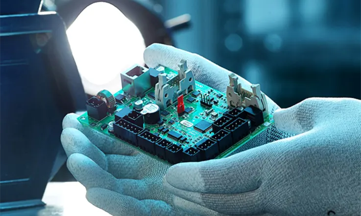
Reverse engineering of printed circuit boards, also known as PCBs, involves the process of duplicating, analyzing, and researching an existing PCB’s design technology. The aim is to understand the product’s processing flow, functional characteristics, structure and technical specifications so that similar products can be manufactured. Reverse engineering originated from hardware analysis in business and the military, often as a means of analyzing finished products and extracting their design principles, since valuable manufacturing information can be challenging to obtain.
At JarnisTech, we offer a range of services, including Printed Circuit Board Reverse Engineering. Utilizing our expertise, we can reverse engineer any given sample, including components, to obtain all the required data for the production of duplicates. Our team is capable of reverse engineering even complex circuit boards with customized parts, programmed integrated circuits, and obsolete components.
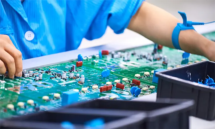
Our reverse engineering process begins by cataloging every electronic component present on the original PCB. A rough bill of materials is then created for the project. Each component is meticulously photographed, and the PCB’s photocopy is enlarged and mounted. Each component is then carefully removed and positioned on the photocopy in its appropriate place. The accuracy of the bill of materials is then refined by measuring resistor and capacitor values.
Once the bill of materials has been finalized, we proceed to source the necessary components. Following this, the circuit board is scanned using a calibrated scanner to duplicate the trace pattern accurately, and brand-new bare boards are manufactured. Before the project is completed, a fully assembled sample is provided to the customer to verify that the product functions as expected. This sample serves as the “golden board,” from which all others will be produced.
What Is Reverse Engineering PCB ?
PCB reverse engineering involves the process of taking an existing printed circuit board (PCB) and creating a schematic diagram and/or a physical replica of it. This is done without access to the original design files or documentation.
The purpose of reverse engineering a PCB may include understanding the function of a legacy board, replicating a discontinued board that is no longer in production, or producing a copy of a competitor’s board for analysis or even for competing with their product. The process involves using a combination of skills in PCB layout, electrical engineering, and software analysis. However, PCB reverse engineering should be done in accordance with the legal and ethical considerations to avoid intellectual property violations.
As we know, Reverse engineering of printed circuit boards (PCBs) is a sophisticated technology that uses a variety of methods and techniques to conduct inverse research. This research technique aims to achieve specific results, including:
● Reverse Bound Constructing.
● Build the Layout.
● Derive Schematics.
Reverse engineering of printed circuit boards (PCBs) has significantly impacted the development of manual and prevalent designs. In the past, creating a new product could take several years, but with PCB reverse engineering technology, it is now possible to develop a new product in just a few months. The field of electronic technology has seen tremendous progress in the last decade, resulting in the development and improvement of numerous products and faster updates for electronic devices.
Many electronics engineering professionals believe that traditional research and development methods may not be successful due to their relatively slow pace compared to the quick turnaround time required by modern electronic device markets. As a result, PCB reverse engineering has emerged as the most effective strategy for keeping up with the rapidly evolving electronic market, which currently has over millions of different manual design iterations.
Reasons for PCB Reverse Engineering
There are several reasons why PCB reverse engineering may be necessary. Some of these reasons include:
● Legacy board analysis: For old technologies where the documentation is lost or has been degraded over time, reverse engineering can help in analyzing the function of the board.
● Replication of Discontinued Parts: In situations where a PCB contains an obsolete component, it may no longer be in production. Reverse engineering can be used to replicate the board, including the outdated or obsolete component, either to continue production or for repair/maintenance.
● Cost reduction: In cases where the original PCB and its documentation are available but the cost to obtain it from an existing supplier is high, reverse engineering can be used to create alternative suppliers.
● Competitive analysis: PCB reverse engineering provides insights into the design and features of a rival’s product, which helps in creating better products or competing effectively.
● Intellectual property protection: Reverse engineering can be used by companies to make sure that their intellectual property is well-protected and not copied by others illegally.
Methods for PCB Reverse Engineering
There are several methods for PCB reverse engineering, including:
● Visual inspection: This involves examining the board carefully to identify individual components, trace connections and their paths. Inspection can be done by eye or using magnifying lenses, microscopes, or cameras.
● Signal tracing: This involves measuring the electrical signals between components to determine their relationship and function. Signal tracing can be done using a multimeter and an oscilloscope.
● X-ray or CT imaging: This non-destructive technique involves visualizing the internal structure of the board, including the trace paths and inner layers, using X-ray or CT scanning.
● De-capping: This involves removing the packaging of integrated circuits, which reveals its internal structure. De-capping can be done using chemicals or using laser technology.
● Circuit extraction: This involves reverse engineering the board using Automated Optical Inspection (AOI) systems to generate CAD data of the PCB layout, including the pin connections, trace paths, and placements of components.
● Cross-referencing: This involves comparing the physical board with known or similar board designs to identify component types, values, and functions.
The chosen method(s) for PCB reverse engineering depends on the complexity of the board and the available equipment and tools that can aid the engineer.
Tools and Equipment Required for PCB Reverse Engineering
The tools and equipment required for PCB reverse engineering may include:
● Multimeter: for measuring electronic signals between components.
● Oscilloscope: for visualizing electronic signals on a waveform graph.
● Logic analyzer: for analyzing digital signals on a circuit board.
● Microscope: for visual inspection of small surface-mounted devices or to read chip markings.
● X-ray or CT scanner: for non-destructive imaging of the components and trace paths.
● Semiconductor analyzer/tester: for testing and analyzing the properties of individual semiconductor components.
● PCB design software: for creating schematics, layouts, and 3D models of the reverse-engineered board.
● CAD software: for generating 3D models or blueprints of the board.
● Chemicals and tools for de-capping: This includes acids, solvents, and tools for removal of the packaging from semiconductor components.
● PCB etching equipment: for creating a replica of the reverse-engineered board.
The specific tools and equipment required may differ depending on the complexity of the board and the reverse engineering technique being used.
How to Select PCB Reverse Engineering Software ?
Selecting the ideal reverse engineering software for a PCB project requires careful consideration of various factors, encompassing budget, project complexity, and available time. Opting for the right tool is crucial to ensure that the venture meets the necessary requirements and is a success. It is prudent to evaluate the pros and cons of each software thoroughly before finalizing the decision.
In selecting the appropriate software, engineers must consider a suite of functions, ranging from computer-aided design (CAD) to computer-aided manufacturing (CAM) and computer-aided engineering (CAE), aimed at the creation of robust circuit designs that maximize functionality. The use of PCB reverse engineering software enhances accuracy and precision, generating manufacturing-ready PCB designs automatically.
For instance, a simple circuit diagram may need only KiCad or DIA software, while a more intricate and complex design may require a combination of CAM, CAE, and CAD software. Effective project outcomes rely on aligning specific project goals with the software features, ease of use, cost, and other factors. It is worth noting that overlooking the software selection process may result in significant errors and production delays.
Regular Flow Process of PCB Reverse Engineering
PCB Reverse Engineering is a process of retroactively investigating the physical components of a printed circuit board (PCB) or its assembly to derive Gerber files and a bill of materials (BOM). The technique is also referred to as PCB cloning or PCB duplication. The information obtained through reverse engineering is utilized to manufacture prototype PCBs, procure necessary components, and assemble PCB prototypes to the desired specifications, matching provided samples. The goal is to replicate the original PCB design utilizing the gleaned information and recreate a functioning prototype as requested by the customer.
The following is PCB Reverse Engineers Regular Flow Process:
● It is recommended to keep a detailed record of each component present on the circuit board, including the models, parameters, and their specific locations for future reference during the reverse engineering process.
● When removing components, it is essential to remove any tin coating on the PAD holes. Adjusting the contrast and brightness of the canvas can reveal differences in appearance between copper-coated and non-coated areas, aiding in the reverse engineering process. Utilize BMP to PROTEL format conversion to prepare two corresponding layers for transmission in PROTEL.
● Further, the BMP file for the TOP layer should be converted to TOP.PCB format. Import both the TOP.PCB and BOT.PCB files into PROTEL software to merge multiple layers into a single image for analysis.
● For accurate analysis, laser printing of the TOP LAYER and BOT LAYER on transparent film is recommended. Place the film over the PCB and assess it for any errors or deviations during the reverse engineering process.
What Do Use Technologies in PCB Reverse Engineering Process ?
● Laser Scanners: Laser scanners are highly regarded as effective 3D scanning technologies commonly used in the process of PCB reverse engineering. This type of scanner captures an image of the PCB using laser light. Laser scanners are well-suited for capturing sophisticated PCB designs with complex geometrical features since they can scan from a variety of angles with high accuracy. In cases where precision and accuracy are critical, laser scanners are the preferred choice for reverse engineering tasks. The use of laser scanning technology ensures that the resulting PCB design replicates the original design with high accuracy, ultimately leading to a successful PCB reverse engineering process.
● Structured Light Source Converters: Structured light scanning technology is another method used to capture a high-resolution image of a printed circuit board (PCB). This technique involves projecting a pattern of lines onto the board and using cameras to capture the reflected light from those lines. Structured light scanners provide higher resolutions compared to laser scanners, which makes them better at capturing minute elements in complicated PCB designs. These features, therefore, make them an excellent fit for recognizing small-sized chips, such as the 0.6 mm ball grid array (BGA). The structured light source converter can effectively detect the BGA, among other intricate details on the PCB, enhancing the accuracy and efficiency of the reverse engineering process.
● X-ray Tomography: X-ray tomography is an effective technology that can be utilized during the reverse engineering process of a printed circuit board (PCB). This method uses an X-ray source to generate a three-dimensional image of the PCB, allowing for detailed information to be collected on the internal layers of the board that may be difficult to obtain using other scanning methods. X-ray tomography proves particularly beneficial in detecting buried components or hidden layers in the PCB, which cannot be visualized using conventional scanning techniques. The generated three-dimensional image empowers engineers to examine intricate details of the PCB and improve the efficiency and accuracy of the reverse engineering process.
How to Reverse Engineer a PCB ?
● Reverse Bound Constructing: To begin reverse engineering a printed circuit board (PCB), it is necessary to acquire precise and well-lit images of both sides of the PCB. These images will serve as the basis for creating a layout to construct a schematic. Initially, a basic board can be chosen, and the layout for constructing the schematic can be drawn on graph paper with symbols representing each component in the circuit. Attention should be given to capture the correct scale to ensure the accuracy of the schematic.
However, for more complex PCBs, relying solely on pencil and paper can lead to confusion and inefficiencies. In such cases, it is advisable to generate a precise line drawing for the PCB, which can then be used to prepare the schematic without requiring additional image editing or color switching.
Although the utilization of images is a time-consuming step that is particularly necessary for more intricate layouts, it is still an essential part of the process. The efficiency of this phase can be enhanced through the use of adequate lighting and a high-quality camera, whether digital or smartphone-based, to capture images of both sides of the PCB.
● Build the Layout: In the case of a more complicated printed circuit board (PCB) that requires extensive photography and editing, creating a schematic will take considerably longer than drawing out the connections manually. For simpler PCBs, one may use a program such as AutoTrace to convert a bitmap image into a vector graphic, by scanning the drawing into the software.
However, the reverse engineering process for a complex PCB will typically involve several modifications stages before a schematic can be constructed. There are various methodologies and programs that can be employed for the reverse engineering of a PCB, but one must be prepared to commit a significant amount of time and attention to the process.
It is necessary to repeat the same methods for both sides of a PCB to build a dual-sided schematic. The editing steps will vary depending on the PCB type, color, and measurements.
● Derive Schematics: The creation of a schematic typically occurs within specialized software programs such as AutoTrace or Target3001!, a PCB layout CAD tool. Once all photo editing and design work is complete, developing the schematic may become the most straightforward phase of the reverse engineering process.
To effectively construct the schematic, it is necessary to merge both PCB sides, utilize component symbols, and arrange tracks logically to ensure easy interpretation. Following this, one must work through the schematic in a step-by-step approach, carefully checking components, replacing lines where needed, and troubleshooting the entire diagram to ensure accuracy.
Note: A potential drawback of reverse engineering printed circuit boards (PCBs) is that it may not always be feasible to determine the origin and endpoints of each connection accurately. It is possible that some tracks, despite appearing to traverse through multiple layers, are connected to internal planes or differently located tracks. If one encounters inconsistencies during the troubleshooting phase, hidden connections may be the source of the issue.
Benefits of PCB Reverse Engineering
Reverse engineering of printed circuit boards (PCBs) provides several advantages for different businesses with varying objectives. For instance, it may be necessary to perform the reverse engineering of a PCB either without documentation or when the available documentation is out of date but is crucial to the organization’s operations. Additionally, reverse engineering can aid in the development of more efficient or cost-effective versions of competitors’ PCB designs.
Find out more about the benefits of PCB reverse engineering by reading the following:
● Get Without Documentation PCB Information: Most modern-day printed circuit boards (PCBs) feature comprehensive documentation or computer-aided design (CAD) data made available to customers. However, encountered in some situations, information pertaining to a given PCB may be inaccessible. In such cases, reverse engineering is an essential process to gather detailed schematic and design information concerning the PCB. Reverse engineering enables the creation of comprehensive documentation on a product, aiding in the understanding of the underlying principles of the product, facilitating its repair or replication.
● ReduceReliance On Experts: In the event of PCB malfunction, contacting a professional for troubleshooting and repair is often the first course of action taken. However, should qualified personnel be unavailable, one may be left in a challenging position due to a lack of understanding of PCB internals. In such instances, reverse engineering offers a viable alternative, enabling individuals to obtain vital information about their PCBs and identify potential issue areas without expert assistance.
● Find theweaknesses in your competitors’ designs: In the business of PCB manufacturing, it is imperative to differentiate one’s products from those offered by competitors. Reverse engineering provides a means to analyze a competitor’s PCB and identify any inefficiencies or weaknesses. Armed with this knowledge, one can enhance the performance of their own PCBs, offering customers a higher value proposition. Moreover, by identifying design flaws within a PCB, one can create boards tailored to specific needs, even if they are not intended for commercial purposes.
● MaintainCrucial PCBs: There are instances in which a designer may possess an outmoded printed circuit board (PCB) that continues to serve a valuable purpose, such as providing electricity to a piece of machinery or an electronic component. Should the PCB fail or require replacement, it may prove difficult to locate a suitable replacement or determine the root cause of the issue. By possessing the ability to reverse engineer an antiquated PCB, designers can potentially maintain essential PCBs for extended periods and even produce clones to serve as replacements in situations where repairs are not feasible.
● ProduceLess Costly PCBs: Reverse engineering of a competitor’s PCB can be useful to determine its actual production cost, particularly when it is being sold at a premium price. In some cases, businesses may charge a premium for PCBs due to a lack of competition. Understanding the true production cost can enable a knowledgeable competitor to create a similar product at a lower price, attracting clients who were previously limited in their options.
Challenges and Limitations of PCB Reverse Engineering
Some of the challenges and limitations of PCB reverse engineering include:
● Time-consuming process: Reverse engineering can be a time-consuming process, especially for boards with complex design or specialized components.
● Difficulty in replicating the circuit function exactly: The original circuit may contain proprietary processes and information, which may be difficult or impossible to reverse engineer completely.
● Limited accuracy of reverse engineering tools: The tools used in reverse engineering, such as X-ray and chemical de-capping, may have limitations in producing accurate results.
● Component obsolescence: Components on the original board may become obsolete or are no longer in production, which can be a major challenge for the reverse engineering process.
● Legal and ethical conflicts: Reverse engineering can be legally and ethically challenging, particularly if it involves intellectual property infringement or violates licensing or contractual agreements.
● Cost: Reverse engineering can be costly, especially if specialized equipment or skills are needed.
● Lack of documentation: The absence of documentation for the original board may limit the accuracy and success rates of the reverse engineering process.
Despite these limitations and challenges, PCB reverse engineering can be a useful tool in various industrial processes and applications.
Applications of PCB Reverse Engineering
The applications of PCB reverse engineering are varied and include:
● Replicating obsolete parts: Reverse engineering can be used to replicate discontinued PCB components, especially where the original manufacturer has stopped producing them.
● Creation of spare parts: Reverse engineering can be used to produce spare parts for a PCB, which can help extend the life of devices that are no longer being produced.
● Quality control: Reverse engineering can be used to check that production PCBs meet the required specifications and standards.
● Intellectual Property (IP) protection: Reverse engineering can be used by companies to protect their IP from infringement by rival companies.
● Product analysis: Reverse engineering can be used to analyze competitor’s products, which can give insights into their design, features, and performance.
● Academic and research purposes: Reverse engineering can be used in academic and research settings for exploring the design principles of PCBs and amplifiers, modeling their performance outcomes, identifying weaker design properties, and developing countermeasures for improving their performance.
● Forensic analysis: Reverse engineering can be used to analyze faulty and failed PCBs to determine the cause of failure and provide recommendations for improvements.
These applications highlight the importance of PCB reverse engineering in various industrial, academic, and research applications.
PCB Reverse Engineering Services: What can we Offer You ?
● JarnisTech offers a range of distinct and varied services for multi-layer PCB reverse engineering and electrical breakdown analysis to meet the unique needs of each customer. JarnisTech has developed the skills and expertise required for deprocessing, cross-sectioning, and electron microscopy through years of experience and experimentation.
● Our team at JarnisTech can provide the necessary data for either a simple cross-section and SEM inspection to identify key process parameters or for a full layer-by-layer deprocessing that includes high-resolution optical and electron microscope images, making it possible to completely reverse engineer a printed circuit board.
● Additionally, JarnisTech can produce SEM mosaic images of large functional blocks at extremely high magnifications, which can be aligned with precision, allowing for signal tracing over multiple layers of the device, making it the most comprehensive solution for PCB reverse engineering services.
● To deliver the most cost-effective and timely results for your specific PCB reverse engineering needs, our specialists analyze the specifications provided and develop customized tests tailored to your requirements. We are equipped to gather essential data needed for your PCB reverse engineering application, whether it be from patent documents, lawyer-specified protocols, or through collaboration with a subject matter expert or circuit extractor.
Legal and Ethical Considerations in PCB Reverse Engineering
PCB reverse engineering can bring up legal and ethical considerations, including:
● Intellectual property infringement: Reverse engineering may infringe on the intellectual property rights of the original manufacturer, especially if it involves proprietary processes or patented components.
● Contractual agreements: Reverse engineering may breach any existing license agreements or other contractual obligations for the product.
● Trademark infringement: Reverse engineering may also infringe on the trademark of an established brand name, especially in cases where the brand name has a distinctive reputation.
● Privacy and security: Reverse engineering may also impact the privacy or security of sensitive or classified information that may be involved in the original PCB.
● Ethical considerations: There may be ethical considerations to take into account, especially if the purpose of reverse engineering jeopardizes the safety, well-being, or privacy of consumers.
● Misuse of information: The reverse-engineered data may be used to make counterfeit products that may pose harm to the end-users, the original manufacturers, or the industry at large.
To responsibly conduct PCB reverse engineering, it is important to carefully consider and address any legal and ethical considerations associated with the process. Seeking legal advice and/or obtaining permission from the original manufacturer before proceeding with reverse engineering may help minimize any potential legal or ethical issues.
Conclusion and Future Outlook on PCB Reverse engineering
PCB reverse engineering is a valuable tool for various industrial, academic, and research applications. While the process can be time-consuming and challenging, the ability to replicate discontinued parts or to analyze competitor’s products make PCB reverse engineering a critical function to ensure a sustainable supply chain and evolution of technology.
However, as with any field, progress in PCB reverse engineering has its challenges and limitations, including legal and ethical considerations surrounding proprietary technology, intellectual property, contracts, privacy, and security.
The continued growth of IoT devices will make PCB reverse engineering even more necessary. As more appliances and devices are integrated with IoT technology, the demand for board-level reverse engineering – to increase reliability and create countermeasures to potential threats – will also grow.
The advancement in computer vision technology, AI-based modeling tools, and machine learning algorithms may facilitate PCB reverse engineering by automating certain aspects of the process, such as component detection and layout recognition.
In conclusion, PCB reverse engineering will continue to be an important tool for extending the lifespan of obsolete equipment, re-creating scarce components, and improving product’s performance by analyzing competitor’s designs. As its applications continue to grow, anticipating and responsibly handling the legal and ethical considerations must remain integral parts of the PCB reverse engineering process.
.


