
Heavy copper PCBs are essential for modern high-power and high-performance applications. These specialized circuit boards, often featuring copper thicknesses ranging from 4 oz to over 200 oz per square foot, are designed to handle higher current loads and better manage heat dissipation. Whether in power electronics, automotive systems, or industrial equipment, heavy copper PCBs provide reliable solutions where traditional PCBs might not suffice.
This guide dives into the key aspects of heavy copper PCB technology, covering everything from material selection and manufacturing techniques to the specific industries where these boards are most impactful. Learn how you can leverage heavy copper PCBs for enhanced performance, durability, and cost efficiency in your next project.
Why Heavy Copper PCBs Are Essential for High-Power Equipment?
Heavy copper printed circuit boards (PCBs) are increasingly becoming the go-to solution for high-power electronics due to their unique capabilities in handling larger current loads and dissipating heat effectively. These PCBs are integral to industrial applications where electrical and thermal stresses are higher than in standard electronic circuits. Heavy copper PCBs allow manufacturers to build equipment that requires higher reliability and longevity under demanding conditions, particularly in environments where electrical and thermal stresses are extreme.
The need for robust PCBs in high-power devices is driven by the growing demand for efficient power management in industries such as renewable energy, automotive, and aerospace. Heavy copper PCBs are particularly beneficial in power-intensive applications, such as electric vehicle charging stations, power supplies, and medical devices, where reliable and continuous operation is required over extended periods.
Key Technologies in Heavy Copper PCBs:
●High Current-Carrying Capacity: Heavy copper PCBs are engineered to carry much higher electrical currents than your standard boards. With copper layers typically starting at 4oz per square foot or more, they’re built to manage larger electrical loads with ease. This design is perfect for heavy-duty applications like power converters and motor drivers, where large currents pass through the board without breaking a sweat. Simply put, these boards are made to take the heat when the power’s on high.
●Superior Thermal Management: One of the primary benefits of heavy copper PCBs is their ability to efficiently dissipate heat. The thick copper layers improve the overall heat conductivity, reducing the chance of overheating and thereby enhancing the longevity of both the PCB and the components it supports.
Enhancing Performance and Reliability
Heavy copper PCBs are designed to handle the intense demands of high-power applications, ensuring stable performance even under high currents and thermal stress. Whether it’s power amplifiers, inverters, or industrial power supplies, these boards keep things running smoothly when it counts. With their ability to manage excessive heat and electrical load, they prevent the kind of breakdowns that could otherwise stall critical operations. In short, heavy copper PCBs take the heat without breaking a sweat, delivering reliable, long-lasting performance when you’re pushing your equipment to the limit.
Heat Dissipation and Copper Thickness-
Copper thickness directly correlates to heat dissipation and electrical resistance. For instance, a 4 oz. copper layer has approximately 35 milliohms of resistance, while a 10 oz. copper layer can reduce that resistance by over 50%, leading to less heat buildup. With better heat conductivity, thermal gradients across the board are minimized, allowing components to work efficiently even under extended high-power loads.
Longevity in Harsh Environments-
Heavy copper PCBs are designed to withstand harsh environments, such as high-vibration areas, extreme temperatures, and exposure to chemicals, which are common in industrial settings. The ability of these boards to handle thermal cycling and mechanical stress without failure is a significant advantage, especially for critical applications like aerospace electronics.
Example: In wind turbine control systems, where temperature fluctuations are common, heavy copper PCBs help ensure that the system operates without frequent maintenance, which directly enhances system uptime and performance.
Reducing Maintenance Costs
One of the most significant benefits of heavy copper PCBs is their durability, which directly correlates with reduced maintenance costs. In high-power equipment, especially in fields like power generation and automotive industries, downtime can be costly. Heavy copper PCBs mitigate frequent repairs and replacements by providing more reliable performance over a longer period.
Resistance to Thermal Stress-
The enhanced heat tolerance of heavy copper PCBs reduces the likelihood of component failure caused by thermal expansion or contraction. These boards are designed to operate within a wide temperature range without degrading, thus minimizing the need for costly repairs due to overheating or thermal damage.
Mechanical Durability-
Heavy copper PCBs are also less prone to mechanical fatigue compared to traditional PCBs. Their robustness makes them ideal for applications in industrial machinery, where vibrations, shocks, and other mechanical stresses are common.
Case Study: A power generation plant using heavy copper PCBs in their electronic control systems found that the boards lasted three times longer than standard PCBs, resulting in a 40% reduction in system maintenance costs over five years.
Enabling Next-Generation Industrial Solutions
Heavy copper PCBs are indispensable in driving the next generation of industrial applications, particularly in the fields of power management, energy systems, and electric vehicles. As industries transition to more energy-efficient technologies, the demand for heavy copper PCBs is expected to grow. These boards support the development of next-gen solutions in the following ways:
Supporting High-Efficiency Power Conversion-
With the advent of more advanced power management solutions, such as DC-DC converters and advanced motor controllers, heavy copper PCBs provide the necessary electrical and thermal support to ensure these devices operate efficiently. These boards help reduce power loss and improve the overall system efficiency of power supplies.
Electric Vehicle and Charging Infrastructure-
Electric vehicles (EVs) and their charging infrastructure require high-performance PCBs that can handle the substantial power requirements of modern batteries and charging systems. Heavy copper PCBs provide the heat resistance and current-carrying capabilities required for both in-vehicle power distribution systems and fast-charging stations.
Power Handling Capabilities of Heavy Copper PCBs vs. Traditional PCBs:
| Copper Thickness | Current Carrying Capacity | Thermal Dissipation Rate | Typical Applications |
| 1 oz/ft² | 5 A | 1 W/cm² | Consumer electronics |
| 4 oz/ft² | 25 A | 2.5 W/cm² | Power converters, EV chargers |
| 10 oz/ft² | 50 A | 4.0 W/cm² | Industrial power supplies, wind turbines |
What Makes Heavy Copper PCBs Unique?
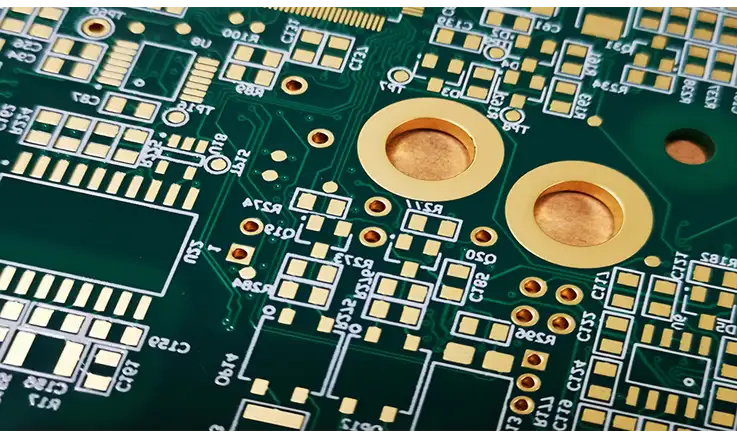
Heavy copper PCBs are distinct from traditional PCBs due to their high copper weight, typically exceeding 4 oz per square foot. The unique properties of these PCBs are crucial for applications requiring high thermal and electrical performance. Heavy copper PCBs are engineered to handle significant amounts of heat and electrical current without compromising reliability or safety, making them ideal for power electronics, industrial machinery, and electric vehicles.
Key Characteristics of Heavy Copper PCBs
Heavy copper PCBs possess key attributes such as high current-carrying capacity, exceptional heat dissipation, and the ability to withstand thermal stress. These attributes make heavy copper boards indispensable for power-heavy applications where traditional PCBs would fail due to heat or mechanical stress.
| Characteristic | Heavy Copper PCB | Standard PCB |
| Copper Thickness | 4 oz – 14 oz per square foot | 0.5 oz – 2 oz per square foot |
| Current-Carrying Capacity | Up to 200 A per channel | Typically below 10 A per channel |
| Thermal Resistance | Lower resistance; better heat dissipation | Higher resistance; prone to heat buildup |
| Application Types | Power supplies, motor controllers, electric vehicles | General consumer electronics, low-power circuits |
Copper Thickness Exceeding 4 oz per Square Foot-
Copper thickness in heavy copper PCBs generally starts at 4 oz per square foot and can go much higher (up to 14 oz or more). This increased copper density ensures a substantial reduction in electrical resistance, leading to better current flow and less heat generation.
In power-sensitive applications, such as renewable energy systems or electric vehicles, the heavy copper layers allow the board to handle high-power loads without overheating. This improvement directly impacts efficiency, making heavy copper PCBs more suitable for applications where heat management is a primary concern.
Applications Requiring Exceptional Heat Dissipation and Durability-
Heavy copper PCBs provide exceptional heat dissipation due to their thick copper layers, making them ideal for high-power applications where heat buildup is a concern. Applications such as motor drivers, power converters, and battery management systems require the ability to transfer heat quickly to prevent system failure. The heavy copper construction ensures that even under prolonged high-load conditions, the board maintains stability.
| Application | Power Dissipation | Copper Thickness | Purpose |
| Electric Vehicles | High | 6 oz – 14 oz | Battery management, motor control |
| Solar Inverters | Moderate to High | 6 oz – 12 oz | Power conversion |
| Industrial Machines | High | 4 oz – 10 oz | Motor drives, power supplies |
Core Benefits for Industrial Applications
Heavy copper PCBs offer numerous advantages in industrial applications, from robust thermal performance to durability under high mechanical stresses. Their enhanced conductivity and strength make them essential for systems that demand long-term reliability, especially in power electronics and automotive sectors.
High Current-Carrying Capacity-
One of the major benefits of heavy copper PCBs is their ability to carry high electrical currents. Standard PCBs typically struggle with high current loads, leading to overheating, trace damage, and eventual failure. However, the thick copper traces in heavy copper PCBs allow for safe, continuous current flow in demanding environments.
For instance, power supplies for electric vehicles (EVs) need to handle currents up to 200 A, which heavy copper PCBs can manage with ease. Additionally, these PCBs are used in high-efficiency power conversion systems in industrial automation, where low resistance is necessary to maximize energy output.
| Application | Required Current Capacity | Copper Thickness | Heavy Copper PCB’s Advantage |
| Electric Vehicles | 150 A – 200 A | 6 oz – 12 oz | Enhanced heat dissipation, higher current handling |
| Industrial Power Supplies | 50 A – 100 A | 4 oz – 8 oz | Reduced thermal buildup, safe power transfer |
Resistance to Thermal Stress and Mechanical Wear-
Heavy copper PCBs are designed to withstand not just electrical stress, but also mechanical and thermal stresses. Due to their thick copper traces, these boards are more resistant to physical damage, including vibration and bending, common in industrial environments. Furthermore, the copper layers provide resistance to thermal cycling—an essential feature for devices that operate in environments with fluctuating temperatures.
Advanced Design Principles for Heavy Copper PCBs
Designing a heavy copper PCB is an intricate process that requires attention to detail in a variety of areas, from selecting the appropriate trace widths to managing heat dissipation. Understanding the complex nature of heavy copper designs allows manufacturers and engineers to craft circuits that not only perform optimally but also stand the test of time in high-stress environments.
Optimizing Trace Widths and Copper Layers
When designing a heavy copper PCB, getting the right trace widths and copper layer thickness is a balancing act. Especially when you’re working on high-current applications, where the efficiency of power distribution can make or break the system’s performance. Traces are the main pathways for electrical current, and with heavy copper designs, managing current without causing excessive heat is key. Too much heat can lead to reliability issues, so it’s all about getting that sweet spot where the PCB can handle the load without breaking a sweat. Getting it wrong could lead to overheating, downtime, and the last thing you want: a fried circuit board. So, precision here isn’t just a good idea—it’s the name of the game!
Designing for High-Current and Power Distribution Efficiency-
In high-current PCB applications, the key is to minimize resistance along the copper traces. To achieve this, design engineers must select copper thickness and trace width according to the expected current load. The thicker the copper layer, the better the PCB will handle higher currents without excessive heating or performance degradation.
In power-sensitive systems like electric vehicles, power inverters, and renewable energy setups, stability in power distribution is a must, especially when these systems are put through tough conditions over long periods. These environments demand reliability, which is where a heavier copper layer—such as 6 oz per square foot or more—really shines. This thickness ensures the PCB can handle high power loads without running into overheating issues. As power flows through these circuits, a thicker copper layer helps prevent the board from becoming a liability, keeping everything from burning out or malfunctioning. In other words, a beefier copper layer does more than just carry current; it keeps the system from overheating, allowing the equipment to function smoothly and without hiccups.
| Copper Thickness | Current Carrying Capacity | Power Distribution Efficiency |
| 4 oz per sq. ft | Up to 60 A | Efficient, common in industrial applications |
| 6 oz per sq. ft | Up to 150 A | Excellent, used in EVs and power inverters |
| 10 oz per sq. ft | 200 A and higher | Optimal for high-power systems |
Additionally, wider traces allow for a more even distribution of current, reducing the likelihood of hotspots where heat can accumulate and cause damage. It’s not just about adding more copper; it’s about strategically optimizing the traces for efficient current flow.
Optimizing Copper Layer Thickness for Performance-
In designing a heavy copper PCB, understanding the relationship between copper thickness and overall performance is key. Thicker copper allows the board to handle more heat and current, but it also affects the board’s weight, flexibility, and cost. The key is striking a balance. If you’re designing for a high-power electric vehicle or industrial motor, thicker copper may be required to handle the significant current and heat dissipation needs. However, a balance must be maintained to avoid excessive material costs or overengineering the solution.
| Design Goal | Recommended Copper Thickness | Impact on Performance |
| Low Power Applications | 4 oz per sq. ft | Standard heat dissipation |
| High Power Systems | 6 oz – 10 oz per sq. ft | High current handling, excellent heat distribution |
| Extreme Power Systems | 12 oz – 14 oz per sq. ft | Exceptional heat dissipation and current-handling ability |
Thermal Management Considerations
Thermal management is one of the biggest challenges when designing heavy copper PCBs. With the ever-growing demand for power in electronic circuits, ensuring the board can handle heat efficiently has become a must. In this section, we will examine the thermal management methods that make heavy copper PCB designs successful.
Role of Thermal Vias and Copper Planes in Heat Dissipation-
Heavy copper PCBs are specifically designed to mitigate the risks associated with overheating. One of the most effective strategies in thermal management is the use of thermal vias. Thermal vias are small copper-plated holes that connect different layers of the PCB, providing a pathway for heat to be transferred from the surface to the inner layers. This prevents localized hotspots from forming and helps dissipate heat more evenly throughout the board.
In addition to thermal vias, copper planes—large, uninterrupted layers of copper—are often used in heavy copper PCBs to spread heat across the entire board. Copper planes are especially useful for high-current applications, as they reduce the electrical resistance that would otherwise cause heat to accumulate along narrow traces.
| Thermal Management Feature | Purpose | Recommended Application |
| Thermal Vias | Heat transfer between PCB layers | Power supplies, electric vehicles, industrial machines |
| Copper Planes | Even distribution of heat | Motor controllers, power converters, battery systems |
| Heat Sinks | External heat dissipation | High-power LED drivers, power inverters |
Best Practices for Thermal Management-
When designing heavy copper PCBs, engineers should think about adding heat sinks or thermal pads to improve heat dissipation. These components can be attached to the copper layers to help transfer heat away from the PCB and into the surrounding air. It’s also wise to pay attention to the layout of the components—ensuring that high-heat areas don’t become too crowded can make a big difference. By spreading things out strategically, you can help the board stay cool and perform better under pressure.
Avoiding Common Design Challenges
Designing heavy copper PCBs comes with its own set of challenges, especially when dealing with high power and high current. There are several common pitfalls that we face during the design and manufacturing phases. Let’s explore some of these challenges and how to avoid them.
Strategies to Prevent Delamination and Over-Etching-
One of the most common issues faced when manufacturing heavy copper PCBs is delamination—the separation of layers within the PCB structure. This usually happens when the copper and substrate layers are not properly bonded, often due to poor material choice or incorrect manufacturing techniques. Delamination can be detrimental, especially when it happens in high-stress areas of the board where high current is flowing.
To prevent delamination, it is essential to use high-quality materials and to control the temperature and pressure during the bonding process. A well-executed lamination process ensures that all layers are properly adhered, providing the strength and thermal resistance needed for high-power applications.
| Issue | Cause | Solution |
| Delamination | Poor lamination process | Ensure correct pressure/temperature, use high-quality materials |
| Over-Etching | Excessive copper removal during manufacturing | Use controlled etching methods to avoid over-etching |
Over-Etching: A Hidden Danger-
Another issue is over-etching, which occurs when the etching process removes too much copper. This can cause circuit traces to weaken or become disconnected, leading to board failure. Ensuring that the etching process is carefully controlled is key to preventing this problem. PCB manufacturers should rely on precise etching technology that maintains tight control over the amount of copper removed.
| Design Issue | Consequence | Prevention Strategy |
| Over-Etching | Weakened or broken traces | Use precise etching processes to control copper removal |
How to Choose the Right PCB Base Materials for Heavy (Thick) Copper PCBs?
When selecting the appropriate base material for thick copper PCBs, several factors need to be considered to ensure optimal performance, durability, and cost-effectiveness. A thick copper PCB, which is typically defined as having copper thicknesses exceeding 4 oz per square foot, requires a base material that can handle the electrical and thermal demands while maintaining structural integrity.
Here’s a breakdown of the factors to consider when choosing the base material for thick copper PCBs:
1. Thermal Management Requirements
Thick copper PCBs are often used in high-power applications that generate significant heat. The PCB base material must support efficient heat dissipation to prevent thermal stress that could damage the PCB. Materials like aluminum, ceramic, and Rogers are commonly chosen for their superior thermal conductivity. For instance, aluminum provides excellent heat dissipation while being cost-effective, making it ideal for consumer electronics. On the other hand, ceramic offers higher thermal conductivity and is commonly used in high-end power applications.
2. Mechanical Strength and Durability
The base material also needs to withstand mechanical stresses and environmental factors like humidity and vibration, particularly in automotive and industrial applications. Polyamide and FR4 (with higher glass transition temperatures) are widely used because of their durability and flexibility. For environments that demand the highest strength, ceramic provides a highly rigid and reliable substrate, perfect for extreme environments.
3. Electrical Performance
Electrical properties, such as dielectric constant and loss factor, play a crucial role in the performance of the PCB. Rogers materials, such as RO4000 and RO3000 series, are engineered for high-frequency applications and offer low signal loss, making them suitable for RF circuits and high-speed designs. Teflon can also be selected for its superior insulation properties and low loss factor in high-frequency environments.
4. Cost Considerations
While some base materials like ceramic offer unmatched performance, they can also come at a high cost. FR4 is a more budget-friendly option, although it may not offer the same level of thermal management or signal integrity as Rogers or Teflon. It’s crucial to balance the material’s performance with the project’s budget constraints.
5. Manufacturing Complexity
Not all base materials are easy to work with when it comes to PCB fabrication. Aluminum and FR4 are relatively easier to process, whereas ceramic requires advanced manufacturing techniques, which can add to the overall cost and time required for production. To keep things efficient and cost-effective, aligning your material choice with what the manufacturer is capable of handling is key. This ensures that production remains on track without any unexpected delays or budget overruns.
Comparison of Base Materials for Thick Copper PCBs-
| Material | Thermal Conductivity | Dielectric Constant | Mechanical Strength | Cost | Best Use Case |
| Aluminum | High (160-200 W/mK) | Moderate (~4.5) | Moderate | Low | General electronics, automotive |
| Ceramic | Very High (up to 180 W/mK) | Low (~10) | High | High | High-power, aerospace, military |
| Rogers | High (up to 300 W/mK) | Low (~3.0) | Moderate | High | High-frequency, RF, telecommunications |
| Teflon | Moderate (0.4 W/mK) | Very Low (~2.1) | Low | High | High-frequency, RF, military |
| FR4 | Moderate (0.3 W/mK) | Moderate (~4.5) | Moderate | Low | Standard applications, low-cost electronics |
When selecting the right base materials for your thick copper PCB, you need to carefully weigh the thermal, electrical, and mechanical properties of the materials. By understanding the specific requirements of your project, whether it’s thermal management, durability, or high-frequency performance, you can make an informed decision. Consider consulting with a PCB manufacturer -(JarnisTech) who specializes in heavy copper PCBs to get expert recommendations tailored to your application.
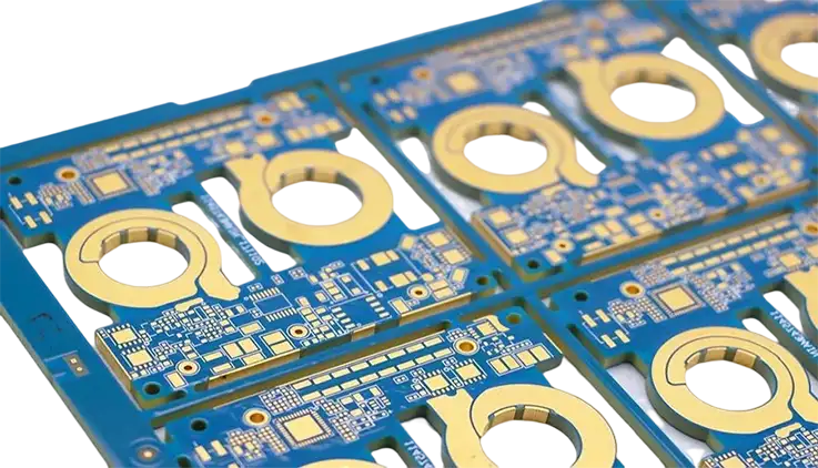
Cutting-Edge Manufacturing Processes for Heavy Copper PCBs
The production of heavy copper PCBs demands precision and a deep understanding of material science and process control. From etching to testing, every step must ensure that these robust boards can handle high currents and extreme temperatures without faltering. Let’s break down the advanced techniques that go into crafting these powerhouses of the PCB world.
Etching and Plating Techniques
When it comes to heavy copper PCBs, standard etching methods don’t cut it. The thicker copper layers require specialized techniques to ensure precise and uniform results. Etching involves removing excess copper from the board, while plating adds copper where it’s needed to form conductive pathways.
Ensuring Uniform Copper Distribution Across Layers-
The process begins by carefully choosing etching solutions and using equipment designed for handling thick copper. For heavy copper PCBs, which often have copper layers of 4 oz/ft² or more, controlling the etching speed is key to preventing issues like undercutting or over-etching. This precise balance ensures the copper is evenly etched, preserving the quality of the final product. Inconsistent etching can result in defects, compromising the PCB’s functionality and reliability, so proper calibration and monitoring throughout the process are necessary to meet design standards.
To address uneven copper distribution, advanced plating techniques, such as pulse plating, are employed. This method ensures a uniform deposition of copper, especially around vias and through-holes. The result? A smoother and more reliable current flow across all layers.
| Etching/Plating Method | Benefits | Applications |
| Conventional Etching | Suitable for up to 3 oz copper | Standard industrial PCBs |
| Pulse Plating | Uniform deposition for thick copper | Heavy copper designs, power systems |
| Differential Etching | Reduces undercutting risk | Multi-layer PCBs with high current |
Case Study: Tackling Uneven Copper Thickness-
In one industrial scenario, a heavy copper PCB for an electric vehicle application faced uneven copper distribution due to inadequate plating. By switching to pulse plating and recalibrating etch times, the manufacturer achieved a uniform layer, boosting the board’s current-carrying capacity by 30%.
Lamination Processes
Laminating a heavy copper PCB is not simply a matter of sticking layers together; it’s about constructing a solid, unified structure that can withstand both mechanical and thermal stress. With thicker copper layers, the process becomes a fine-tuned challenge. Achieving a strong bond between layers while ensuring the integrity of the copper itself demands attention to detail. The combination of heat, pressure, and time needs to be perfectly balanced to ensure the layers adhere without compromising the overall performance of the board.
Handling Thick Copper Without Compromising Layer Adhesion-
The lamination process involves layering pre-preg sheets (reinforced fiberglass material soaked in resin) between copper layers, followed by applying heat and pressure to bond them. For heavy copper boards, the process requires adjustments in pressure to accommodate the thicker copper while preventing resin starvation—a condition where the resin doesn’t flow adequately to bond layers.
| Pressure Setting | Copper Thickness | Risk Mitigated |
| Standard Pressure | <3 oz copper | Suitable for standard PCBs |
| Medium Pressure | 4–6 oz copper | Reduces resin starvation |
| High Pressure | 10 oz or more | Ensures complete layer bonding |
Advanced Resin Formulations-
To improve adhesion and thermal performance in heavy copper PCBs, specialized resin systems are often employed. High-Tg (glass transition temperature) resins, for example, are engineered to ensure that the board retains its structural strength even when exposed to higher temperatures. This is a must-have for applications such as industrial motor drives or power inverters, where temperature fluctuations are common. By using these resins, we can ensure that the PCB stands up to the heat and mechanical stress, maintaining reliability in demanding environments.
Pro Tip: Laminating heavy copper boards is like making a multi-layered sandwich; you’ve got to get the pressure and “spread” just right, or it all falls apart under stress.
Quality Assurance and Testing
Once a heavy copper PCB has been manufactured, rigorous quality control measures ensure it can handle real-world demands. From thermal performance testing to electrical reliability checks, every board must pass the test—or it doesn’t leave the factory.
Thermal Performance Testing-
For heavy copper boards, thermal management is a top priority. Testing involves subjecting the PCB to high current loads and monitoring its heat dissipation capability. This is typically done using thermal imaging cameras to identify hotspots and confirm that copper layers and vias are functioning as intended.
| Test Type | Purpose | Tools Used |
| Thermal Cycling Test | Simulates repeated heating/cooling | Thermal chambers |
| Heat Dissipation Test | Measures temperature rise under load | Thermal imaging cameras |
Electrical Reliability Checks-
Electrical testing ensures that all traces, vias, and connections on the PCB meet the design specifications. For heavy copper boards, high-current testing is performed to verify that the board can handle its rated load without any breakdowns.
Example: Load Testing for Industrial Applications
In one instance, a heavy copper PCB designed for an industrial power supply was subjected to a 200 A load during testing. By monitoring voltage drops across traces and measuring thermal performance, we were able to certify the board for use in high-stress environments.
Pricing Dynamics of Heavy Copper PCBs
Understanding the pricing structure for heavy copper PCBs can feel like peeling back layers of an onion—each layer reveals new variables influencing the cost. By breaking down the key drivers and offering strategies to optimize expenses, we aim to shed light on how you can make smarter procurement decisions without cutting corners on quality.
Factors Influencing Cost
The cost of heavy copper PCBs is influenced by a variety of factors, including the choice of materials, the complexity of the design, and the manufacturing processes involved. These elements combine to determine the overall price tag, and each step—from selecting copper thickness to choosing specialized resins—adds its own layer of cost.
Copper Thickness and Layer Count-
Copper isn’t just a material—it’s a commodity with fluctuating market prices. The heavier the copper, the more expensive the PCB. A board with 10 oz of copper per square foot will naturally cost more than one with a standard 1 oz layer. Add to that the number of layers, and you’re looking at exponential increases.
| Copper Thickness (oz/ft²) | Average Cost Increase (%) | Applications |
| 1 oz | Baseline | Consumer electronics |
| 3 oz | +30% | Industrial controllers |
| 6 oz | +75% | High-power inverters |
| 10 oz | +150% | Electric vehicle systems |
Board Complexity-
Simple designs with fewer traces and vias are cheaper to produce. When the board involves intricate layouts for high-power distribution, costs ramp up due to the need for precision etching and plating processes.
For instance, a multilayer heavy copper PCB for an industrial power supply might require extensive tooling and testing, leading to higher costs.
Manufacturing Technology-
Production facilities equipped with state-of-the-art technology for thick copper processing can reduce waste and improve yield, but these savings may not always trickle down to the customer, depending on the scale of the order.
Example: A manufacturer specializing in heavy copper boards might use pulse plating and automated etching equipment, which minimizes material wastage and speeds up production, but upfront setup fees can make small batch orders pricey.
Strategies for Cost Optimization
Cutting costs doesn’t have to mean sacrificing quality. There are proven ways to balance durability and performance with budget constraints.
Streamlining Design for Manufacturing-
Designing with manufacturability in mind is a smart move. Here’s a cheat sheet for optimizing your design without breaking the bank:
●Simplify Layer Counts: Stick to the minimum number of layers required for your application.
●Optimize Copper Usage: Use thicker copper only where necessary. For example, limit high-current paths to specific regions rather than applying it across the entire board.
●Standardize Dimensions: Use panel sizes that align with the manufacturer’s capabilities to reduce material waste.
Bulk Orders for High-Volume Production-
Ordering in bulk is a no-brainer when working with heavy copper PCBs. Large volumes allow manufacturers to spread setup costs across multiple units, significantly reducing the per-unit price.
| Order Quantity | Average Cost per PCB (6 oz Copper) |
| 10 units | $250 |
| 100 units | $175 |
| 500 units | $120 |
Partnering with Specialized Manufacturers-
Choosing a fabricator with experience in heavy copper PCB production can save money in the long run. These specialists understand the nuances of handling thick copper, ensuring fewer errors and better quality at competitive rates.
Tip: Ask your supplier about cost-saving options like alternative materials or modified processes tailored to your project’s needs.
Comparing Costs Across Manufacturers
When it comes to pricing, not all PCB fabricators are created equal. Expertise, geographic location, and facility capabilities can lead to notable cost differences.
Expertise Drives Efficiency-
An experienced manufacturer can deliver consistent quality while minimizing material waste. This efficiency often translates into lower costs, particularly for complex designs.
| Manufacturer Type | Cost Variability | Ideal For |
| General PCB Fabricator | Moderate to High | Standard boards with light copper |
| Heavy Copper Specialist | Low to Moderate | High-power, heavy-duty designs |
| High-Tech Facility | High upfront, low long-term | Advanced, multi-layer heavy copper |
Impact of Geographic Location-
Offshore manufacturers often offer lower labor costs, but the trade-off might include longer lead times or communication barriers. On the other hand, local suppliers may charge a premium for quicker delivery and personalized support.
Case Study: Cost Comparison Across Suppliers-
A renewable energy company sourcing 6 oz copper PCBs compared quotes from three suppliers:
1. Local Manufacturer: $190/unit, lead time: 2 weeks.
2. Offshore Specialist: $150/unit, lead time: 5 weeks.
3. Global Manufacturer with Bulk Discount: $120/unit for 500+ units, lead time: 3 weeks.
The company chose the global supplier due to its combination of competitive pricing and reasonable lead times for bulk production.
Comparing Heavy Copper PCBs to Ceramic and Metal Core PCBs
Choosing the right PCB for industrial applications often requires weighing the strengths of heavy copper PCBs against alternatives like ceramic and metal core PCBs. Each option has its place in specific scenarios, dictated by their performance under high-temperature conditions, durability in harsh environments, and their best-suited use cases.
Performance Under High-Temperature Conditions
Heavy copper PCBs, ceramic PCBs, and metal core PCBs are all engineered to handle heat dissipation, but their effectiveness can vary significantly based on application demands.
Thermal Conductivity-
●Heavy Copper PCBs: These excel in applications requiring efficient heat spreading across large current paths, thanks to thick copper layers. However, copper’s thermal conductivity, while good, is outpaced by ceramic substrates.
●Ceramic PCBs: Made from materials like aluminum oxide or nitride, ceramic PCBs boast exceptional thermal performance. Their low coefficient of thermal expansion also ensures dimensional stability under extreme heat.
●Metal Core PCBs (MCPCBs): These typically incorporate aluminum or copper cores, providing focused heat dissipation for localized high-power components.
| PCB Type | Thermal Conductivity (W/mK) | Best Application |
| Heavy Copper PCB | 385 | Industrial power equipment |
| Ceramic PCB | 200-350 | Aerospace and LED systems |
| Metal Core PCB | 130-200 | High-intensity lighting, automotive |
Electrical Performance-
Heavy copper boards maintain consistent electrical performance in power-heavy environments, whereas ceramics shine in applications requiring high-frequency stability. MCPCBs balance electrical performance and thermal management but might lack the current-carrying capacity of heavy copper options.
Durability in Harsh Environments
When it comes to standing up to tough conditions, each PCB type offers unique advantages.
Mechanical Resilience-
●Heavy Copper PCBs: These are practically built like tanks, handling mechanical stress without flinching. They’re ideal for equipment subjected to vibration or physical shock.
●Ceramic PCBs: Ceramic substrates are naturally brittle, making them more susceptible to cracking under heavy stress. However, their ability to withstand chemical exposure and radiation is unmatched.
●Metal Core PCBs: Offering a sweet spot between strength and flexibility, MCPCBs are well-suited for rugged applications like automotive electronics.
Longevity-
Heavy copper PCBs are a top choice for systems requiring extended operational lifetimes, particularly in environments with fluctuating temperatures. Ceramics, while less robust mechanically, remain operationally stable for long periods in niche scenarios, such as satellite systems or medical equipment.
Use Case Differences
Understanding where each PCB excels can simplify the selection process.
Heavy Copper PCBs-
Used primarily in high-power applications like industrial control systems, renewable energy converters, and electric vehicle inverters, these boards are designed to handle substantial current loads. They’re a go-to for projects requiring durability and efficiency.
Ceramic PCBs-
The aerospace industry, high-frequency communication devices, and high-powered LEDs are some of the key sectors relying on ceramic PCBs. Their thermal and electrical properties make them indispensable for specialized applications.
Metal Core PCBs-
MCPCBs are favorites in the lighting industry, particularly for high-intensity LEDs. Automotive sectors also lean heavily on these boards for engine control systems due to their thermal management capabilities.
| Use Case | Heavy Copper PCB | Ceramic PCB | Metal Core PCB |
| Industrial Equipment | ✔High durability | ❌ Brittle | ✔Moderate durability |
| High-Power LEDs | ✔Good for power distribution | ✔Optimal thermal management | ✔Affordable thermal solution |
| Automotive Electronics | ✔Handles high currents | ❌ Limited mechanical strength | ✔Reliable heat dissipation |
When deciding between heavy copper, ceramic, and metal core PCBs, the answer lies in the specific demands of your project. Heavy copper PCBs dominate where durability and current capacity are non-negotiable. Ceramics step in for applications demanding precision under extreme heat and radiation, while MCPCBs strike a balance for cost-effective thermal management.
Still undecided? Let’s chat! Our team can guide you through selecting the best PCB for your unique needs. Whether you’re designing for industrial power systems or advanced LED arrays, we’ve got the expertise to keep your projects running like a well-oiled machine. Reach out today and let’s make it happen!
Why Choose Us for Your Heavy Copper PCBs?
When you’re looking to build heavy copper PCBs, it’s not just a simple process—it’s a specialized skill that requires top-notch technology and a keen understanding of the intricacies involved. Heavy copper PCBs demand attention to detail, as they need precise copper layers and complex manufacturing methods, making them more challenging (and expensive) than regular circuit boards. But, rest assured, the payoff is more than worth the extra investment when you see the final product’s performance.
With over 20 years of experience in the PCB industry, JarnisTech has positioned itself as a leading PCB manufacturer and turnkey PCB assembly provider in China. We specialize in creating high-quality heavy copper PCBs, from fast-turn prototypes to small and medium-volume productions. Our commitment is to deliver not only precision but also top-notch service, ensuring that your heavy copper PCB meets the highest standards.
Our Heavy Copper PCB Manufacturing Capabilities
Our capabilities in the following areas have helped us grow into one of the most reputable copper-rich printed circuit boards producers in China:
| Specification | Details |
| Base Material | FR/4 all TGs, Aluminum, Ceramic, Rogers, Teflon, Polyamide, Copper, etc. |
| Copper Thickness | 4 Oz – 10 Oz |
| Extreme Heavy Copper | 20 Oz – 200 Oz |
| Soldermask | Yellow, Red Oil, Green, Blue, Black, White |
| Surface Finishing | Immersion Gold (ENIG), OSP, HASL |
| Outline | Punching, Routing, V-Cut |
| Maximum Number of Layers | 60 |
| Finished Thickness | 0.020ʺ – .275ʺ |
| Minimum Soldermask Clearance | 5 MIL |
| Minimum Solder Dam Width | 5 MIL |
| Vias | Blind and Buried Vias |
| Holes | Minimum Drill Bit Hole Size: .012ʺ |
| Minimum Hole Size: .008ʺ +.005ʺ/- .008ʺ | |
| Maximum Hole Aspect Ratio = 12:1 | |
| Controlled Impedance | +/- 5% |
| Minimum Silkscreen Line Width | 7 MIL |
Whether you need prototypes or full-scale production, our team goes above and beyond to meet your expectations, making sure your boards are built to last. At JarnisTech, we’re dedicated to the details, offering a seamless process and ensuring the end product exceeds your requirements. So, if you’re looking for reliability, expertise, and a partner that understands the intricate needs of heavy copper PCBs, we’ve got your back.
Let’s get your project on track—reach out to JarnisTech today for your heavy copper PCB needs!
Heavy Copper PCB & FAQ
What industries commonly use heavy copper PCBs?
Heavy copper PCBs are primarily used in industries that require high current-carrying capacity and effective thermal management. These industries include power electronics, automotive (especially electric vehicles), industrial machinery, medical devices, and renewable energy systems such as solar power and wind energy.
What are the differences between heavy copper PCBs and regular copper PCBs?
The primary difference lies in the thickness of the copper layers. Heavy copper PCBs feature copper thicknesses exceeding 4 oz per square foot, whereas standard PCBs typically use thinner copper. This increased copper thickness enhances their ability to handle higher power densities, making them ideal for power electronics and high-current applications.
Can heavy copper PCBs be used in high-frequency applications?
Heavy copper PCBs are not typically recommended for high-frequency applications. Their thicker copper layers can lead to increased inductance and reduced signal integrity, making them less suitable for high-speed or high-frequency signals compared to standard PCBs designed for RF applications.
How does the cost of heavy copper PCBs compare to traditional PCBs?
Due to the increased copper thickness and more complex manufacturing processes required, heavy copper PCBs are generally more expensive than standard PCBs. The cost is influenced by factors such as copper thickness, board complexity, and the specific manufacturing techniques used, such as advanced etching and plating.
What are the typical thicknesses of copper used in heavy copper PCBs?
The thickness of copper in heavy copper PCBs typically ranges from 4 oz to 12 oz per square foot. In some specialized cases, copper thicknesses can go as high as 20 oz per square foot, depending on the application’s power and thermal requirements.
Can heavy copper PCBs be used in flexible or rigid-flex circuits?
Heavy copper PCBs can be used in flexible or rigid-flex designs, but their increased copper thickness may make the board stiffer and harder to bend, especially when compared to standard flexible PCBs. The flexibility of the PCB must be carefully considered during the design and manufacturing process to ensure compatibility with the desired application.
How can I ensure the thermal performance of a heavy copper PCB?
To ensure optimal thermal performance, designers should incorporate thermal vias, copper planes, and other thermal management strategies during the design phase. The use of copper in the PCB structure helps distribute heat efficiently, while thermal vias connect different layers to enhance heat dissipation. Additionally, the use of high-quality materials and manufacturing processes that minimize defects is critical for maintaining thermal efficiency


