
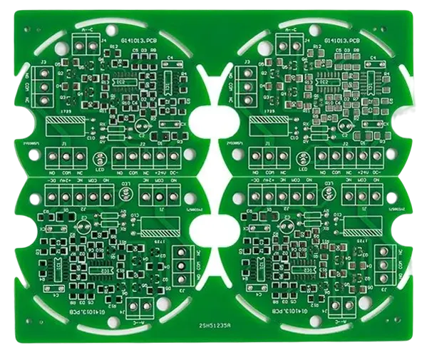
When you think about the guts of any electronic device, from smartphones to medical equipment, the prototype PCB is right at the heart of it all. A Printed Circuit Board (PCB) serves as the backbone of virtually every electronic product today. But in the complex world of product development, prototype PCB design isn’t just a phase — it’s the testbed where ideas are turned into reality. Whether you’re designing a consumer device, an industrial machine, or an automotive component, the prototype stage is where innovation meets precision engineering.
By now, the importance of having a reliable prototype PCB can’t be overstated. Think about it: it’s where functionality is validated, where all the hard work of circuit design, material selection, and assembly processes come together. In short, it’s where great ideas either succeed or fail. In this guide, we’ll dive deep into the design, manufacturing, assembly, and testing of prototype PCBs—and we’ll break down the process step by step, so you can bring your ideas to life and avoid common pitfalls.
The Prototype PCB Lifecycle
Creating a high-performing PCB prototype is much like tuning a finely crafted instrument—it demands precision, expertise, and an eye for detail. From the earliest sketch on paper to the final testing phase, the journey of a prototype PCB is a critical part of modern electronics. This lifecycle not only ensures reliable functionality but also offers invaluable feedback for product optimization.
Why Prototype PCBs Are Essential for Your Product’s Success?
PCB prototyping serves as the proving ground for any electronics project, acting as the foundation where concepts take shape and real-world functionality is tested. By putting these prototypes through exhaustive trials, you can catch design flaws and fine-tune performance well before committing to mass production. Forgoing this step can lead to expensive errors or products that fail to meet reliability standards, which could tarnish your project’s reputation and bottom line. It’s like building a house—you’d want to inspect the blueprint before laying bricks, saving yourself from potential headaches down the line.
Case Studies in Innovation Testing-
Take Apple, for instance. With every iPhone release, engineers iterate on PCB designs multiple times. Each prototype undergoes extensive thermal and signal integrity testing to support high-speed processors and optimize battery life. Similarly, Tesla incorporates prototype PCBs into its energy-efficient vehicle systems, using them to refine power management and sensor accuracy.
Key Benefits of Prototyping for Product Success-
| Benefit | Application | Example |
| Early Flaw Detection | Identifying issues with design or material compatibility | Apple’s signal integrity testing for iPhones |
| Improved Efficiency | Reducing power losses and optimizing component layout | Tesla’s PCB testing for battery management |
| Better Performance Insights | Validating high-frequency circuits and EMI shielding | 5G communication hardware prototyping |
Don’t let your next innovation stall because of skipped steps. Prototype like a pro—test, refine, and perfect!
The Life of a Prototype PCB: From Sketch to Final Board
The development of a PCB prototype is like building a puzzle—every piece needs to fit perfectly. The process involves several interconnected stages, each with its unique challenges and tools. Below is a roadmap from concept to reality.
The End-to-End Development Process-
1.Concept and Design: Engineers start by defining the functionality and requirements of the PCB, often using advanced CAD tools like Altium Designer or KiCad.
2.Schematic Capture: The electrical design is transferred into a schematic diagram, detailing connections between components.
3.PCB Layout: This phase involves placing components on a board and routing connections, using 3D visualization tools for precision.
4.Fabrication: Boards are manufactured using processes like photolithography, etching, and solder masking.
5.Assembly and Testing: Components are mounted onto the board, and rigorous functional testing is performed.
Traditional vs. Modern Prototyping Methods-
| Stage | Traditional Approach | Modern Approach | Advantages of Modern Techniques |
| Design | Manual sketches | CAD tools with simulations | Speeds up design and reduces errors |
| PCB Layout | Hand-routing | Automated routing with 3D previews | Improves accuracy, optimizes space usage |
| Fabrication | Hand-built models | CNC and photolithography machines | Reduces manufacturing time |
| Testing | Manual inspections | Automated test systems (e.g., X-ray) | Detects issues with higher precision |
If you’re still relying on the old-school methods, it’s time to shake things up. Modern tools are here to save you time and headaches.
Understanding the Hidden Challenges in Prototype PCB Development
No matter how top-notch your tools and skills are, you’ll likely face some bumps in the road when developing PCB prototypes. Whether it’s a sudden shortage of materials, design missteps, or unexpected tweaks required to meet performance standards, these issues can throw a wrench in the works. Even with a solid plan, some things just don’t go as expected, which means staying flexible and troubleshooting on the fly is a must to keep things moving forward. It’s all part of the game when bringing ideas to life!
Top Challenges in PCB Prototyping-
1.Material Procurement Delays: Sourcing high-quality materials, especially for multilayer PCBs, can be time-consuming. For example, shortages of copper or high-frequency laminates have impacted delivery schedules worldwide.
2.Design Errors: Even minor missteps in routing or component placement can lead to signal integrity issues or power losses.
3.Fabrication Bottlenecks: Tight deadlines and insufficient capacity at fabrication facilities often delay project timelines.
Challenges and Solutions in Prototype PCB Development-
| Challenge | Description | Solution |
| Material Sourcing | Delays in acquiring rare or expensive materials | Partner with reliable suppliers offering quick-turn options |
| Design Iterations | Errors in schematic or layer stack design | Use design simulation tools like SPICE |
| Testing Complexity | Overlooking edge-case testing scenarios | Invest in automated testing systems (ATE) |
What Is Prototype PCB?
The journey of a prototype PCB doesn’t simply begin when you place the first component on a board. It’s a carefully crafted cycle that intertwines design, testing, feedback, and iteration. Each phase contributes to ensuring the final product can meet not only performance requirements but also cost-efficiency, reliability, and manufacturing scalability. Therefore, Prototype PCBs serve as experimental platforms, enabling we to test concepts, troubleshoot flaws, and refine designs before committing to mass production.
The Role of Prototype PCBs in Product Development
Prototype PCBs act as the testing grounds for new designs. They allow teams to try out, adjust, and fine-tune circuits before scaling up to mass production, helping to save both time and money. The prototype phase also provides a chance to identify potential issues early on, preventing costly mistakes that could delay product launches. Think of it as a chance to test the waters before diving in, ensuring everything is set for smooth sailing when it’s time to go into full production.
Key Contributions of Prototype PCBs-
●Testing Early Concepts: Engineers can evaluate the functionality of circuits at an early stage. For example, testing a power management module on a PCB prototype can verify its ability to handle specified current loads without overheating.
●Iterative Refinement: A prototype can undergo multiple iterations to address challenges such as signal interference, impedance mismatches, or inadequate power delivery. For instance, RF designs for telecommunications often require fine-tuning through multiple prototypes.
●Pre-Production Validation: Before transitioning to production, the prototype serves as a final checkpoint. Manufacturers test aspects like solder joint reliability, thermal performance, and high-speed signal integrity.
Example: Medical Devices
Consider wearable heart monitors, where accuracy is non-negotiable. Prototype PCBs help verify the analog front-end circuit’s sensitivity, ensuring it can detect faint electrical signals from the heart without noise interference. A single oversight at this stage could compromise patient safety.
| Stage | Purpose | Outcome |
| Conceptual Testing | Evaluate circuit functionality | Identify and fix early design flaws |
| Iterative Refinement | Optimize layout and material choices | Resolve thermal and electrical issues |
| Pre-Production Validation | Verify manufacturability and performance | Ready-to-scale, high-reliability design |
Key Features of Prototype PCBs
Designing prototype PCBs requires a sharp focus on both design and material selection, as these decisions directly affect the board’s functionality, performance, and how smoothly it can be mass-produced. The features that distinguish prototype PCBs are rooted in these key considerations. This process involves balancing the need for flexibility in design with the durability and cost-effectiveness of materials. Whether it’s using specialized substrates to optimize signal integrity or considering thermal management, each element plays a role in ensuring the prototype functions as expected and can transition into large-scale production with minimal hiccups.
Design Complexity-
Modern prototype PCBs often incorporate multi-layer stack-ups to support advanced technologies. For example, a 12-layer PCB used in automotive radar systems will feature controlled impedance traces, blind/buried vias, and copper pours for power delivery. Achieving such complexity demands CAD tools like Altium or KiCad.
Material Selection-
Prototypes often require specialized materials for unique applications:
●High-Frequency Applications: Use low-dielectric-loss materials like Rogers 5880 for RF circuits.
●Flexible Applications: Employ polyimide-based substrates for wearable devices.
●Thermal Management: Aluminum-backed PCBs are common in high-power LEDs and EV battery systems.
| Material Type | Typical Application | Key Properties |
| FR-4 | General-purpose consumer electronics | Low-cost, moderate performance |
| Rogers 4000 Series | High-frequency RF circuits | Low loss, excellent thermal performance |
| Polyimide | Flexible/wearable electronics | High flexibility and thermal resistance |
Common Applications of Prototype PCBs
Prototype PCBs are at the heart of innovation across many industries, playing an integral part in bringing new ideas to life. These boards serve as the testing ground for emerging technologies, helping designers perfect their concepts before moving to full production. From consumer electronics to medical devices, automotive systems to telecommunications, prototype PCBs are there to refine the design, ensuring everything works like a charm.
Below are examples of how they support diverse applications:
Consumer Electronics-
Smartphones, tablets, and gaming consoles all rely on prototype PCBs during development. Engineers test features like touchscreen responsiveness, signal integrity for high-speed connections (e.g., USB 4.0), and battery management systems.
Automotive Industry-
Advanced Driver Assistance Systems (ADAS), battery management for EVs, and in-vehicle infotainment systems all require extensive prototyping. For instance, radar modules in autonomous vehicles demand highly precise PCB layouts with controlled impedance and low-loss materials.
Medical Devices-
Prototype PCBs are essential in wearable health monitors, portable diagnostic equipment, and implantable devices. Engineers test circuit stability under varying operating conditions, such as fluctuating temperatures or electrical interference in hospital environments.
The Design Process for Prototype PCB: From Schematic to Layout
Designing a prototype PCB is a blend of technical precision and creative problem-solving, requiring thorough planning and flawless execution. From converting a rough circuit design into a schematic to fine-tuning the physical layout for optimal performance, each phase is crucial in creating a board that is not only reliable but also ready for mass production. The process involves striking a balance between innovation and practicality, ensuring that the final product can withstand real-world conditions without compromising on efficiency. Every decision, from component placement to trace routing, shapes how the PCB will function, making it a solid foundation for successful designs that are both manufacturable and high-performing.
Initial Schematic Design for Prototype PCBs
Schematic design forms the backbone of any prototype PCB project, representing the logical connections between components. At this stage, the focus is on functionality and accuracy, as errors in the schematic can cascade into costly problems downstream.
Key Steps in Schematic Design-
1.Component Selection:
●Selecting the right components lays the groundwork for achieving your design objectives. For instance, incorporating a 32-bit microcontroller with built-in peripherals can simplify the development process for IoT projects by reducing the need for additional external modules. This approach streamlines integration, minimizes board space, and lowers overall system complexity. Think of it as choosing the perfect tool for a DIY project—having the right features at your fingertips can save time and effort while delivering a cleaner, more efficient result.
●Designers often refer to manufacturers’ datasheets and industry tools like Digi-Key’s Part Selection Wizard to ensure compatibility and availability.
2.Footprint Libraries:
●Ensuring precise footprints for components is a must when aiming for an accurate PCB layout. Software like Altium Designer or KiCad comes loaded with robust libraries to streamline the process, but certain situations—such as working with proprietary or less common components—might call for custom footprints. Taking the time to design these from scratch guarantees compatibility and avoids issues during assembly.
3.Schematic Capture Tools:
●Leading software tools like OrCAD, KiCad, and Altium Designer are used to capture the schematic. These platforms provide features such as ERC (Electrical Rule Checking) to catch design errors early.
Example:
Imagine developing a wearable health device prototype. During schematic capture, we must carefully choose ultra-low-power components, such as sensors and microcontrollers, to maximize battery life. Missing a decoupling capacitor in the schematic could lead to erratic power fluctuations.
| Task | Tools/Resources | Considerations |
| Component Selection | Digi-Key, Mouser | Cost, availability, lead times |
| Schematic Capture | Altium, KiCad | Compatibility with manufacturing processes |
| Footprint Verification | IPC standards, custom libraries | Accuracy for assembly and testing |
Layer Stackup and Signal Integrity in Prototype PCBs
Layer stackup design is one of the most intricate aspects of PCB prototyping, particularly for high-speed or high-frequency circuits. Signal integrity is a key focus, as issues like crosstalk or impedance mismatches can degrade performance and reliability.
Layer Stackup Design-
●A prototype PCB might use a 4-layer stackup for simple designs or up to 12 layers for complex applications like automotive radar.
●Designers must balance cost, manufacturability, and performance. For example, burying power and ground planes within inner layers reduces electromagnetic interference (EMI).
Techniques for Signal Integrity-
●Impedance Matching: Maintaining consistent impedance for signal traces is a cornerstone of designing for high-speed signal integrity. This involves meticulous adjustments to factors such as trace width, the gap between adjacent traces, and the dielectric properties of the PCB substrate. A well-tuned impedance ensures minimal signal reflection, reduced distortion, and reliable data transfer, particularly in demanding applications like high-frequency RF systems or gigabit Ethernet. It’s like balancing a seesaw—one misstep in dimensions or materials can throw the entire system out of sync.
●Via Optimization: High-frequency signals can suffer reflections or losses due to poorly designed vias. Using blind or buried vias minimizes signal distortion in complex layouts.
| Layer | Purpose | Example Design |
| Top Layer | Signal Routing | High-speed traces for PCIe or USB connections |
| Inner Layer 1 | Power Plane | VCC distribution for microcontrollers |
| Inner Layer 2 | Ground Plane | Reduces EMI and provides a clean reference |
| Bottom Layer | Signal Routing | Low-speed signal lines |
Example Application:
For a prototype 5G antenna PCB, maintaining signal integrity in the GHz range requires materials like Rogers 5880 and precise impedance control. A poorly designed stackup can result in signal losses and reduced bandwidth.
Prototype PCB Design Challenges
Designing a prototype PCB often requires overcoming challenges related to physical constraints, including compact board dimensions, optimal component placement, and effective heat management. Addressing these issues early in the design process paves the way for a prototype that meets performance expectations without unnecessary setbacks.
Size Constraints-
Compact designs, such as those for IoT or wearable devices, demand creative solutions to fit all components within limited space. For instance, using rigid-flex PCBs allows engineers to fold parts of the circuit to save space.
Thermal Dissipation-
Managing heat in high-power applications, such as LED drivers or automotive circuits, demands precise thermal strategies. Incorporating features like thermal vias helps disperse heat from hotspots to broader areas, while aluminum-backed PCBs improve heat transfer due to their conductive properties. These solutions keep temperatures under control and safeguard consistent operation, even under demanding conditions.
Managing Complexity-
Advanced prototype PCBs may include a mix of digital, analog, and RF signals, which requires careful partitioning and shielding. Simulation tools like Ansys SIwave are often used to validate designs.
Common Challenges and Solutions-
| Challenge | Solution | Example |
| Compact Layouts | Use rigid-flex PCBs | Wearable health devices |
| Heat Management | Add thermal vias, heatsinks | High-power LED drivers |
| Mixed-Signal Design | Partition and shield analog/RF areas | IoT gateways with Wi-Fi and Bluetooth modules |
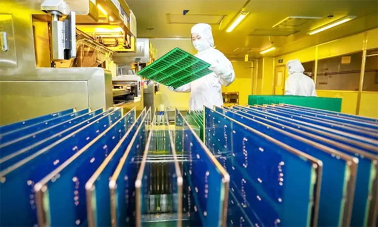
Prototype PCB Manufacturing: Methods and Materials
Creating prototype PCBs requires a careful blend of material choices, precision manufacturing, and effective production scheduling. These elements all play into delivering a functional, high-quality board that can be smoothly transitioned to mass production. By grasping the nuances of each factor—whether it’s the right materials for durability, the exact measurements for efficient performance, or timelines that keep the project moving—we can produce prototypes that don’t just meet design goals but also streamline the process for scaling up. Getting this balance just right ensures that the prototypes are both cost-effective and ready to perform in a real-world environment.
Key Materials for Prototype PCB Fabrication
Choosing the right substrate and laminate material is the foundation of any successful PCB prototype. These materials directly impact the board’s electrical efficiency, long-term reliability, and how well it performs in specific applications. We need to consider factors like cost, operating frequency, and heat dissipation when making their selections. Whether you’re working on a high-speed design or something with higher thermal demands, getting the material choice right can make all the difference.
Popular Materials Used in Prototype PCBs-
1.FR-4:
●Widely used due to its affordability and versatility.
●Suited for general-purpose designs like consumer electronics.
●Thermal performance can vary with grades, making it ideal for basic to mid-complexity designs.
2.High-Frequency Laminates:
●Designed for RF and microwave applications.
●Materials like Rogers 4350B and Isola I-Tera MT40 offer low dielectric loss, ensuring signal integrity at higher frequencies.
●Commonly used in telecommunications, radar systems, and 5G prototypes.
3.Metal-Core and Aluminum Substrates:
●Excellent for thermal management in LED lighting and power converters.
●Aluminum-backed PCBs dissipate heat more effectively, ensuring stable operation in high-power applications.
Material Comparison-
| Material | Advantages | Common Applications | Cost Factor |
| FR-4 | Cost-effective, versatile | Consumer electronics, wearables | Low |
| High-Frequency Laminates | Signal integrity, high-speed data | Telecom, aerospace, 5G devices | Medium to high |
| Aluminum Substrates | Thermal dissipation | LED lighting, power electronics | Medium |
Advanced Manufacturing Techniques for Prototype PCBs
As design complexities continue to grow, modern prototype PCB manufacturing leans heavily on cutting-edge techniques to ensure precision and reliability. These advanced methods enable engineers to push the envelope in terms of functionality, allowing for the development of intricate, high-performance boards. With tighter tolerances and more demanding requirements, PCB manufacturers are adopting innovative processes that not only meet these needs but also drive efficiency in production. This combination of skill and technology is the key to delivering prototypes that are ready for the next stage of development, ensuring that designs can be tested and fine-tuned quickly.
Techniques in Use-
1.High-Density Interconnect (HDI):
●Employs microvias and blind/buried vias to connect densely packed layers.
●Ideal for compact devices like smartphones or smartwatches where space is at a premium.
2.Rigid-Flex Manufacturing:
●Combines the flexibility of flexible circuits with the rigidity of standard PCBs.
●Useful for prototypes where circuits need to fold or bend, such as in aerospace or medical devices.
3.Automated Fabrication:
CNC drilling, laser direct imaging (LDI), and automated optical inspection (AOI) ensure accuracy.
Reduces human errors, streamlining the prototyping process for multi-layer or complex boards.
Example:
A startup working on a compact drone controller may opt for HDI techniques with microvias to fit high-performance processors and sensors onto a small footprint. Automated fabrication ensures all connections are flawless, enabling quicker debugging and revisions.
| Technique | Features | Applications | Example Industry |
| HDI | Microvias, compact routing | Compact prototypes, IoT devices | Consumer Electronics |
| Rigid-Flex | Durable, foldable designs | Aerospace, medical devices | Aviation, Healthcare |
| Automated Fabrication | Precision and speed | Multi-layer prototypes | All industries |
PCB Prototyping Lead Times and Quick-Turn Solutions
When it comes to prototype PCB development, time is often a huge factor. With many manufacturers offering fast-turnaround services, we can speed up their iterations and test new ideas quickly during the product development phase. This means shorter design cycles, allowing teams to meet tight deadlines and adjust designs based on real-world testing before committing to mass production. Quick-turn solutions provide the flexibility to move faster, helping to streamline the development process while still maintaining the quality and performance required for successful prototypes.
Lead Times for Prototyping-
●Standard prototype PCBs may take 5-7 business days to fabricate.
●Quick-turn options deliver boards in as little as 24-48 hours, albeit at a higher cost.
●Selecting a local manufacturing partner can reduce shipping delays, making it easier to meet project timelines.
Rapid Prototyping Services-
●Companies like JarnisTech provide specialize in quick-turn PCB manufacturing.
●They often provide value-added services like design-for-manufacturability (DFM) reviews, ensuring that designs align with fabrication constraints.
Case Study: Meeting Tight Deadlines-
A medical device manufacturer developing a handheld diagnostic tool faced a tight timeline to meet regulatory testing. By leveraging a quick-turn service, they received prototype boards within 48 hours, enabling the team to identify and resolve design flaws ahead of their next milestone.
Standard vs. Quick-Turn Prototyping-
| Feature | Standard Prototyping | Quick-Turn Prototyping |
| Lead Time | 5-7 business days | 24-48 hours |
| Cost | Lower | Higher |
| Suitable For | Projects with flexible schedules | Time-sensitive projects |
Testing and Validation of Prototype PCBs: Ensuring Quality and Reliability
Testing prototype PCBs is the defining step to ensure they perform reliably and meet design expectations under realistic and extreme conditions.. Comprehensive testing not only helps identify manufacturing hiccups but also validates that the design can stand up to real-world challenges—whether that’s extreme heat, fluctuating voltages, or interference from nearby components. By putting prototype PCBs through their paces in varied environments,we can be confident that the design holds up, making adjustments as needed before moving to production. This stage guarantees that, come launch day, the product won’t let you down, and all the kinks have been ironed out.
In-Circuit Testing (ICT) for Prototype PCBs
In-Circuit Testing (ICT) is a diagnostic process that evaluates individual components and connections within a PCB assembly. Unlike functional testing, which assesses the board as a whole, ICT dissects the circuit on a granular level, ensuring every element matches the design.
Advanced ICT Techniques-
1.Boundary-Scan Testing:
●Used for boards with limited physical test points.
●Leverages JTAG protocols to test chip-to-chip connections digitally.
2.Flying Probe Testing:
●Ideal for low-volume or prototype production.
●Probes move across the board without requiring a dedicated test fixture, reducing setup time.
Practical Applications:
ICT is particularly beneficial during the early stages of prototyping. For example, in a multi-layer high-speed PCB designed for radar systems, ICT can detect defects like unconnected vias or incorrect resistor placements. We often prioritize ICT because correcting these errors in later production stages would significantly increase costs.
| ICT Parameter | Purpose | Example Tool/Method |
| Short Circuit Detection | Ensures no unintended pathways | Flying Probe Systems |
| Resistance Measurement | Verifies resistor values | JTAG Boundary-Scan |
| Component Verification | Confirms capacitors, diodes, etc. | Bed of Nails Fixture |
Functional Testing for Prototype PCBs
Functional testing goes beyond simple checks to simulate real-world conditions and gauge how a PCB holds up in action. We need carefully test the board’s interactions with its environment and connected devices, looking for any performance hiccups like signal interference or power drops that might fly under the radar with basic testing. This hands-on approach helps uncover issues that wouldn’t show up in static tests, giving us the real deal before moving forward in production.
Detailed Workflow-
1.Simulation Setup:
●Load the operational firmware and connect the board to necessary hardware (sensors, actuators, etc.).
●Introduce variable inputs (e.g., voltage fluctuations, signal modulations) to simulate operational environments.
2.Evaluation Criteria:
●For PCBs used in high-speed networks or data centers, signal speed and integrity are key factors to ensure smooth communication and data flow. Any interruptions, like signal degradation or delays, can cause performance issues or even system crashes.
●Power integrity analysis ensures that fluctuating loads won’t destabilize the voltage supply to critical ICs.
Case Study:
A team developing a wearable medical device performed functional testing to validate signal clarity and power consumption. By simulating body heat and movement conditions, they adjusted the PCB’s power management IC to reduce unnecessary energy usage while maintaining reliable sensor performance.
| Testing Aspect | Key Metric | Example Measurement |
| Signal Integrity | Crosstalk, jitter | Eye Diagrams |
| Power Efficiency | Voltage stability, power draw | Load Transient Analysis |
| System Responsiveness | Reaction times, accuracy | Time Domain Reflectometry |
Environmental Testing of Prototype PCBs
Environmental testing exposes prototype PCBs to harsh operating conditions to validate their robustness and durability.This step is non-negotiable, especially for PCBs used in critical industries like aerospace, automotive, and industrial automation, where a malfunction isn’t an option. From high heat to intense vibration, these tests confirm that the board can handle the toughest situations without breaking a sweat.
Critical Environmental Stress Tests-
1.Thermal Shock Testing:
●Alternates between extreme temperatures in rapid succession.
●Identifies issues such as solder joint cracking due to thermal expansion mismatches.
2.Vibration and Mechanical Shock:
●Applies vibrations and mechanical impacts to test the board’s resilience in transit or operation.
●Essential for automotive or military-grade PCBs.
3.Corrosion and Moisture Testing:
●Simulates high-humidity environments to test for long-term corrosion and electrical leakage.
Technical Example:
When developing a PCB for a space exploration project, we subjected prototypes to vacuum conditions combined with extreme temperature cycling. These tests revealed that standard solder paste was insufficient, leading to the adoption of a high-reliability silver-tin alloy.
| Environmental Test | Conditions Simulated | Outcome |
| Thermal Cycling | -40°C to +125°C, 500 cycles | Identifies solder joint fatigue |
| Vibration Stress | 10–500 Hz sine vibration | Ensures structural integrity |
| Humidity Test | 95% RH at 85°C for 48 hours | Detects electrical leakage |
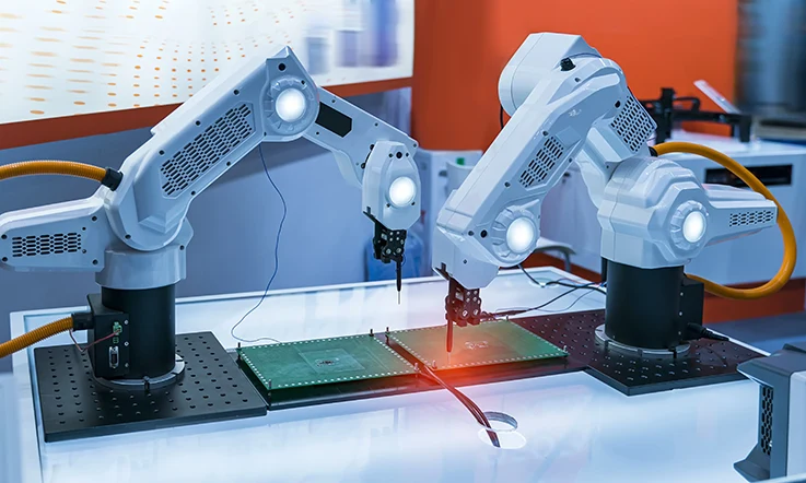
Prototype PCB Assembly: Best Practices and Techniques
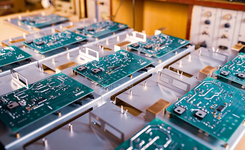
Efficient assembly of prototype PCBs bridges the gap between design validation and mass production. This phase demands precision and adaptability to ensure every component functions as intended. Here, we dive into methods, challenges, and inspection techniques that define a robust prototype PCB assembly.
SMT and Through-Hole Assembly for Prototype PCBs
The assembly process is the backbone of any prototype PCB, determining not just its functionality but also its manufacturability at scale. Among the most discussed methods are Surface-Mount Technology (SMT) and Through-Hole Technology, both serving distinct purposes depending on the application. Their adoption often depends on the type of components, the intended use case, and the required performance metrics.
Surface-Mount Technology (SMT)-
●Components are mounted directly onto the surface of the PCB.
●Used for high-density designs, enabling compact layouts and faster assembly.
Through-Hole Technology-
●Components with leads are inserted through holes in the PCB and soldered on the opposite side.
●Preferred for prototypes requiring strong mechanical connections or components that endure environmental stresses.
Choosing the Right Method-
For example, SMT is widely adopted in consumer electronics prototypes due to its ability to handle miniaturized components, such as microprocessors and ICs. In contrast, automotive prototype PCBs for power systems might incorporate through-hole components for connectors or high-current elements.
| Feature | SMT Assembly | Through-Hole Assembly |
| Component Size | Suitable for micro and nano components | Limited to larger components |
| Mechanical Strength | Moderate | Excellent (e.g., for large transformers) |
| Production Speed | High (automated placement) | Slower (manual or hybrid assembly) |
| Application | High-frequency circuits, IoT devices | Aerospace, power electronics, automotive |
Best Practices for Component Placement-
●Thermal Relief Strategies: Components sensitive to heat should be distanced from heat sources like voltage regulators.
●Symmetrical Layouts: Prevents solder joint stress by maintaining balanced thermal distribution during reflow soldering.
●Stencil Design for Solder Paste: Precision in stencil apertures ensures consistent solder deposition for reliable SMT connections.
Assembly Process Challenges for Prototype PCBs
Prototype assembly isn’t without its fair share of hurdles. We face a unique mix of challenges, from sourcing rare components to navigating design constraints introduced by evolving standards or customer requirements. Understanding these obstacles and adopting proactive measures can drastically improve the assembly experience and results.
Challenges in Component Availability-
The ongoing global component shortage has intensified the complexity of prototype PCB assembly. We often face extended lead times for specialized ICs or resistors, forcing design revisions mid-project.
Solution: Leverage substitute components or modular PCBs for interchangeable designs. For example, in consumer electronics prototyping, we frequently design placeholder footprints for multiple capacitor types to counter supply unpredictability.
1.Yield Rates and Assembly Errors
Achieving high yield rates in prototypes can be challenging due to the manual nature of low-volume assembly. Errors like solder bridging or misplaced components are common.
| Common Issue | Cause | Solution |
| Solder Bridging | Excess solder paste | Optimize stencil design and solder volume |
| Misaligned Components | Human error in manual placement | Use semi-automated pick-and-place equipment |
| Open Circuits | Incomplete soldering | Reflow profiling and AOI (Automated Optical Inspection) |
2.Automation vs. Manual Assembly
●Manual Assembly: Ideal for low-volume prototypes with varied components but prone to inconsistencies.
●Automated Assembly: High accuracy with SMT but may require additional investment in setup for one-off prototypes.
Quality Assurance in Prototype PCB Assembly
Even the most carefully assembled PCB prototype can harbor defects, whether due to soldering inconsistencies, misaligned components, or unforeseen interactions between layers. Quality assurance bridges the gap between assembly and functionality, ensuring that prototypes not only work but perform reliably under intended conditions.
1.Automated Optical Inspection (AOI)-
●Uses high-resolution cameras to detect misplaced components, soldering issues, and polarity errors.
●Example: AOI detected a reversed diode in a prototype power PCB, preventing a potential short circuit during functional testing.
2.X-ray Inspection-
●Analyzes solder joints in hidden areas, such as beneath Ball Grid Array (BGA) packages.
●Essential for prototypes with complex multilayer assemblies.
3.Functional Testing (Post-Assembly)-
●Power-on tests validate the overall circuit operation.
●Ensures components such as oscillators and power ICs function under simulated conditions.
| Inspection Method | Purpose | Application |
| AOI | Detects physical defects | SMT-heavy designs |
| X-ray | Examines internal solder connections | BGA or CSP components |
| Functional Test | Validates full circuit operation | Prototypes with complex circuitry |
Pricing and Cost Considerations for Prototype PCB Manufacturing
Managing costs in prototype PCB manufacturing is an intricate balance of quality, performance, and budgetary constraints. Purchaser and manufacturers alike must consider various factors that influence costs, from design complexity to supplier selection. Let’s break down the key considerations and practical approaches to optimizing expenses without compromising on results.
Factors That Impact Prototype PCB Pricing
When it comes to the cost of prototype PCBs, you’re looking at a mix of factors that all pile on to the final price.It’s influenced by multiple technical and production factors, each adding to the overall expense. Understanding these factors can empower teams to make informed decisions, ensuring every dollar spent contributes to achieving their project goals.
1.Design Complexity-
●Complex circuits with higher pin counts and densely packed components demand more sophisticated fabrication techniques, raising costs.
●Additional features like blind vias, buried vias, or controlled impedance add layers of complexity and cost.
2.Material Selection-
●FR-4 remains a popular, cost-effective material, but high-frequency laminates, ceramic substrates, or metal-core PCBs for thermal management are considerably pricier.
●The choice of solder mask and copper thickness also contributes to material expenses.
3.Layer Count and Board Size-
●A single-layer board is inexpensive compared to multilayer boards, especially those exceeding six layers.
●Larger board dimensions or irregular shapes can lead to higher scrap rates, driving up material costs.
4.Production Volume-
●Producing a single prototype incurs higher costs per unit compared to small-batch or mass production due to the setup costs associated with machinery.
Prototype PCB Pricing Influences
| Factor | Impact on Cost | Example |
| Design Complexity | Higher with advanced features like blind vias | HDI PCBs with 10+ layers for 5G applications |
| Material Choice | Increases with specialty substrates | High-frequency laminates for RF circuits |
| Layer Count | Multilayer boards cost more than single-layer ones | 8-layer boards for data servers |
| Production Volume | Lower per unit cost for higher quantities | Small-batch runs for medical device prototypes |
Cost-Effective Prototyping Solutions
In a world of tight budgets and short timelines, finding affordable yet reliable prototyping solutions has become a priority. Striking the right balance between cost and quality demands creative strategies, including sourcing, technology, and workflow optimization.
1.Leveraging Offshore Suppliers-
●Offshore manufacturers, particularly in regions like Asia, offer competitive pricing for both materials and fabrication.
●While cost savings are significant, one must ensure thorough communication and clear specifications to avoid delays or errors.
2.Automated Manufacturing Processes-
●Automation reduces human error and streamlines production, lowering labor costs. For instance, automated optical inspection (AOI) and SMT pick-and-place machines drastically improve efficiency.
3.Choosing Standard Panel Sizes-
Opting for industry-standard sizes minimizes material wastage, translating to savings.
4.Prototype Aggregation Services-
●Some manufacturers offer pooled prototype services, where boards from different projects share a single manufacturing panel, reducing setup costs.
Cost-Reduction Strategies
| Strategy | Benefit | Consideration |
| Offshore Manufacturing | Lower unit costs | Possible language barriers or longer lead times |
| Automation | Reduced labor costs and higher precision | Initial setup costs for automated systems |
| Standard Panel Sizes | Less material wastage | Limited flexibility in board dimensions |
| Pooled Prototype Services | Shared costs for low-volume production | Restricted customization |
How to Manage Prototyping Budgets for PCB Projects?
PCB prototyping budgets tend to expand unexpectedly, especially when hidden costs surface. To keep things under control, it’s all about planning ahead and managing resources efficiently. By mapping out every step and keeping an eye on details—like material choices, design intricacies, and deadlines—you can prevent the budget from ballooning out of proportion. This way, you ensure the project stays within limits without cutting corners on quality. It’s like playing it smart with your cash while still achieving top-tier results.
1.Early Cost Analysis-
●Start with a detailed breakdown of expected costs, factoring in design revisions, material choices, and assembly methods.
●Use online cost calculators provided by PCB manufacturers for initial estimates.
2.Sourcing Strategies-
●Maintain a list of multiple suppliers to mitigate risks of shortages or pricing spikes.
●Consider domestic suppliers for critical, quick-turn projects and offshore ones for lower costs on non-urgent orders.
3.Mitigating Unexpected Expenses-
●Set aside a contingency budget to handle unforeseen issues, like design corrections or expedited delivery.
●Collaborate with experienced engineers or consultants to identify potential problem areas during early design stages.
4.Cost Efficiency in Iterations-
●Instead of producing multiple full prototypes, create partial or modular prototypes for testing specific features, reducing overall expenses.
Prototyping Budget Management
| Budgeting Strategy | Advantage | Potential Challenges |
| Early Cost Analysis | Clearer picture of expenses | Requires time and effort to research |
| Multiple Suppliers | Flexibility in sourcing | Coordination with multiple vendors |
| Contingency Budget | Preparedness for unexpected costs | Increased initial budget allocation |
| Modular Prototyping | Lower cost for iterative testing | Limited testing of full-system functionality |
Why Choose Us for Your Prototype PCB Needs?
At JarnisTech, we specialize in manufacturing prototype PCBs that meet the high demands of precision electronic devices. With technology advancing at lightning speed, the need for efficient, sustainable, and cost-effective PCB solutions is more pressing than ever. That’s where we step in—with a state-of-the-art production facility designed to help you hit the market faster and stay ahead of the competition.
1.Advanced Technology Tailored for Complex Requirements
Our expertise spans a wide range of cutting-edge technologies, from high-density HDI multi-layer PCBs to rigid-flex boards. Whether it’s telecom, medical, automotive, or any other industry, we’re equipped to meet even the most specialized requirements. Our innovative approach allows us to handle everything from micro-core designs to large GEM PCBs, ensuring your prototypes meet the exact specifications needed for performance and reliability.
2.Top-Notch Materials from Trusted Suppliers
We source materials exclusively from leading names such as Rogers, Shengyi, Wazam, Dupont, Rohm & Haas, and Atotech. By working with these suppliers, we ensure that your PCBs are built with materials optimized for durability, performance, and long-term value. Our team carefully evaluates every material to ensure it’s the best fit for your unique project needs.
3.Fully Independent Production Line for Precision and Quality
When you work with JarnisTech, you’re investing in quality that stands the test of time. Our independent production line is equipped with the latest tools and technology, allowing us to maintain strict oversight and deliver consistently high-quality products. From initial design to final assembly, every step of the process is handled with the utmost care to ensure your satisfaction.
4.Our PCB Prototyping and Small-volume Production Capabilities
We refuse to waste your time since we realize the value of it. To speed up assembly, JarnisTech will effectively communicate with your assembly facility to identify the most efficient panel format. Our complete turn-key PCB assembly service will allow for 24 to 48-hour turnaround times for PCB prototypes.
| PCB Order Quantity (Area) | Original Lead Time (Days) | Current Lead Time (Hours) |
| 0-50 pcs & < 1m² | 2–3 Days | 24 Hours |
| 1m² – 5m² | 5–6 Days | 3–4 Days |
| 5m² – 10m² | 6–7 Days | 4–5 Days |
| More than 10m² | 8–10 Days | 5–6 Days |
We excel in efficiency rate and offer a one-stop service for all of your PCB prototype assembly requirements. We’ll even do a DFM (Design to Manufacturabillity) test upon your request. By preparing the boards for production once prototypes have been tested and endorsed by our customers, JarnisTech can ease the transition from prototype to production. Our processes allow your products to be tested rapidly and introduced to the market in a much faster manner.
FAQ & Prototypes PCB
1. What is the difference between a prototype PCB and a production PCB?
A prototype PCB is designed for testing and validation during the early stages of product development, while a production PCB is the final version that is mass-produced. Prototype PCBs typically use fewer layers and might have less stringent design specifications, whereas production PCBs are optimized for high-volume manufacturing and may require stricter quality control.
2. How long does it take to manufacture a prototype PCB?
The timeline for manufacturing a prototype PCB can vary depending on the complexity of the design, materials used, and the production method. Typically, prototypes can be produced in as little as 24 hours for simple designs, but more complex boards with multiple layers may take 5–10 days to complete.
3. Can I use the same PCB design for both prototypes and mass production?
While it is possible, it’s not always ideal. Prototype PCBs often undergo modifications after testing, which may necessitate redesigns before transitioning to mass production. Furthermore, mass production typically involves adjustments for efficiency, cost reduction, and scaling that aren’t necessary in the prototype phase.
4. What types of testing are involved in prototype PCB development?
Common tests for prototype PCBs include in-circuit testing (ICT), functional testing (to check performance in real-world conditions), and environmental testing (to assess how the PCB handles heat, moisture, and physical stress). These tests help identify design flaws and ensure the final product meets all required specifications.
5. What is the role of a PCB manufacturer in prototype development?
PCB manufacturers play a key role in prototype development by offering expertise in design optimization, providing high-quality materials, and ensuring precision during the fabrication process. They also help manage lead times and advise on cost-effective solutions while adhering to technical requirements.
6. What materials are typically used in prototype PCBs?
Common materials for prototype PCBs include standard FR4 for general-purpose designs, high-frequency laminates for RF circuits, and aluminum PCB substrates for high-power applications. The choice of material depends on the functionality and intended application of the PCB.
7. Are there any common mistakes to avoid when designing a prototype PCB?
Some common mistakes include poor component placement, not considering thermal management, using incompatible materials, and failing to plan for test points or debugging. These issues can lead to manufacturing delays and additional costs.


