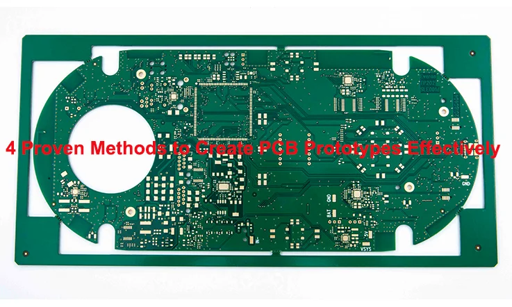
Whether you’re a newbie designer looking to bring your first PCB to life or a seasoned engineer refining your latest project, prototyping is where your ideas hit reality. With PCB designs becoming more complex, selecting the right prototyping method can make or break your process. This guide will walk you through four of the most reliable methods for PCB prototyping, helping you decide which works best for your unique project. Along the way, we’ll explore detailed steps, pros and cons, and show how each method stands out, ensuring you get your prototype right the first time.
This guide will walk you through four tried-and-true methods for PCB prototyping: DIY fabrication, utilizing PCB design software, outsourcing the process, and employing rapid prototyping techniques. Each method has its own unique flair and fits different needs, so let’s dive into the nitty-gritty!
Method 1: DIY PCB Fabrication: The Hands-On Approach
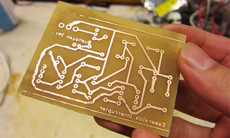
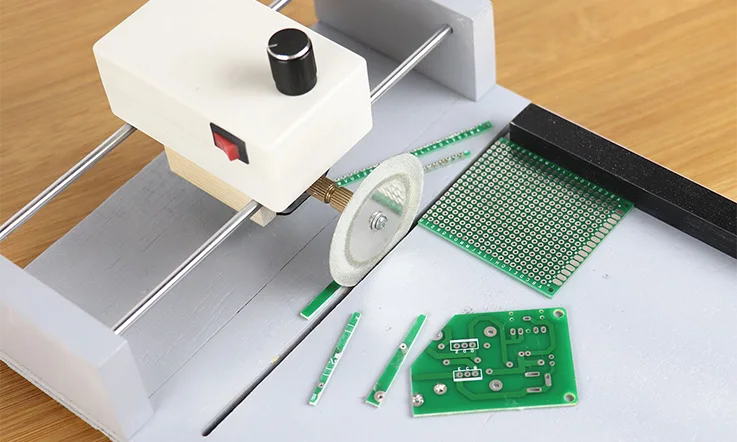
DIY PCB fabrication is akin to cooking your favorite meal from scratch. You get to pick the ingredients, follow the recipe, and, in the end, enjoy the fruits of your labor. This approach appeals to many electronics enthusiasts because it allows for complete control over the design and manufacturing process. Additionally, it can be a fun and educational experience, especially for those who love to tinker.
Essential Tools and Materials
Before you jump into the deep end, you’ll need to gather some essential tools and materials. Here’s a quick rundown:
● Copper-clad board: This is the substrate where your circuit will be etched.
● Etching solution: Ferric chloride is a popular choice for removing unwanted copper.
● Soldering iron: A trusty soldering iron is essential for assembling your components.
● Design software: Even if you’re going DIY, software like KiCAD can help you create your circuit layout.
● Drill: A small drill (around 1mm) is necessary for making holes for component leads.
● Protective gear: Safety first! Gloves and goggles will keep you safe from chemicals and heat.
Step-by-Step Guide to DIY PCB Fabrication
1)Design Your Circuit: Start with a schematic using your favorite PCB design software. This is the blueprint for your project, so take your time to ensure everything is in place.
2)Print the Design: Once you’re satisfied with the design, print it onto a transparency sheet or directly onto the copper-clad board using a laser printer.
3)Prepare the Copper Board: Clean the copper board with fine sandpaper or steel wool to remove oxidation. This helps the etching process work more effectively.
4)Transfer the Design: If you printed on a transparency, you’ll need to expose the board to UV light. If you printed directly, you can skip this step.
5)Etch the Board: Immerse the board in the etching solution and gently agitate it. In a matter of minutes, you’ll start to see the unwanted copper dissolve away.
6)Rinse and Drill: Rinse the board with water and drill holes for your components.
7)Solder Components: Finally, place your components in the holes and solder them in place. Voila! You’ve got yourself a DIY PCB.
Pros and Cons of DIY PCB Fabrication
Pros:
Cost-effective: You can save money, especially for small batches.
Complete control: You decide every aspect of the design and fabrication process.
Learning experience: It’s a great way to deepen your understanding of electronics.
Cons:
Time-consuming: DIY can take a while, especially if you’re new to the process.
Room for error: Mistakes can occur, and troubleshooting can be a hassle.
Skill level required: It may be challenging for complete beginners.
Method 2: Utilizing PCB Design Software: Streamlining the Process
Using PCB design software is like having a top-notch GPS for your road trip; it guides you through the twists and turns of design and fabrication. This method is especially popular among both newbies and seasoned pros because it simplifies the design process and enhances accuracy.
Top PCB Design Software Options
When it comes to PCB design software, there are several options to consider. Here’s a quick look at some of the best out there:
● Eagle: Known for its user-friendly interface, Eagle is great for beginners and has plenty of tutorials available.
● KiCAD: This is a free, open-source option that offers a robust set of features, perfect for DIY enthusiasts.
● Altium Designer: A professional-grade software that provides advanced capabilities, suitable for large-scale projects.
Designing Your PCB: A Step-by-Step Approach
1)Choose Your Software: Select the PCB design software that suits your needs and install it.
2)Create a New Project: Start a new project, and familiarize yourself with the interface.
3)Schematic Capture: Draw your circuit schematic using the software’s tools. This will be the foundation of your PCB layout.
4)PCB Layout Design: Convert your schematic into a PCB layout. The software will help you place components and route traces automatically.
5)Design Rule Check (DRC): Run a DRC to catch any potential errors before fabrication.
6)Generate Gerber Files: These files are what manufacturers use to produce your PCB. Make sure to double-check them!
7)Send to Manufacturer: Choose a reliable PCB manufacturer and send your Gerber files for production.
Advantages and Limitations of Software Design
Advantages:
● Precision: Software eliminates errors associated with manual design.
● Easy modifications: You can quickly make changes without starting from scratch.
● Simulation: Many programs offer simulation features to test your design virtually.
Limitations:
● Learning curve: Some software can be complex for beginners.
● Cost: While some options are free, others can be pricey.
● Dependency on technology: You’ll need a computer and the necessary software to get started.
Method 3: Outsourcing PCB Prototyping: When to Leave it to the Experts
Sometimes, you just gotta know when to fold ’em. Outsourcing PCB prototyping can be a smart move, especially for businesses looking to scale up production or those tackling complex designs. This approach allows you to leverage the expertise of seasoned professionals.
How to Choose a PCB Manufacturer?
Selecting the right PCB manufacturer can feel like finding a needle in a haystack. Here are some key factors to consider:
● Quality: Look for manufacturers that use high-quality materials and have a track record of producing reliable products.
● Cost: Get quotes from multiple manufacturers to compare costs. Just be careful not to compromise quality for a lower price.
● Turnaround time: Ensure the manufacturer can meet your deadlines. Fast isn’t always better, but you don’t want to be left hanging either.
● Customer support: A responsive manufacturer can make all the difference, especially if issues arise during production.
The Outsourcing Process: A Step-by-Step Guide
1)Research Manufacturers: Compile a list of potential manufacturers based on reviews, recommendations, and your specific needs.
2)Request Quotes: Contact the manufacturers and request quotes based on your design specifications.
3)Review Samples: If possible, ask for samples of their previous work to assess quality.
4)Place Your Order: Once you’ve chosen a manufacturer, place your order and provide them with your Gerber files.
5)Communication: Keep the lines of communication open during production. This will help address any potential issues before they escalate.
6)Receive and Inspect Your PCBs: Once you receive your PCBs, inspect them thoroughly to ensure they meet your specifications.
Pros and Cons of Outsourcing
Pros:
● Expertise: You benefit from the knowledge and skills of seasoned professionals.
● Time-saving: Manufacturers can often produce PCBs faster than you could on your own.
● Scalability: Outsourcing allows you to scale production without investing in additional resources.
Cons:
● Less control: You relinquish some control over the manufacturing process.
● Communication barriers: Misunderstandings can occur if you’re not clear about your requirements.
● Cost: Outsourcing can be more expensive than DIY methods, especially for small batches.
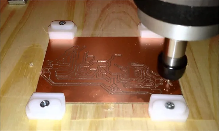
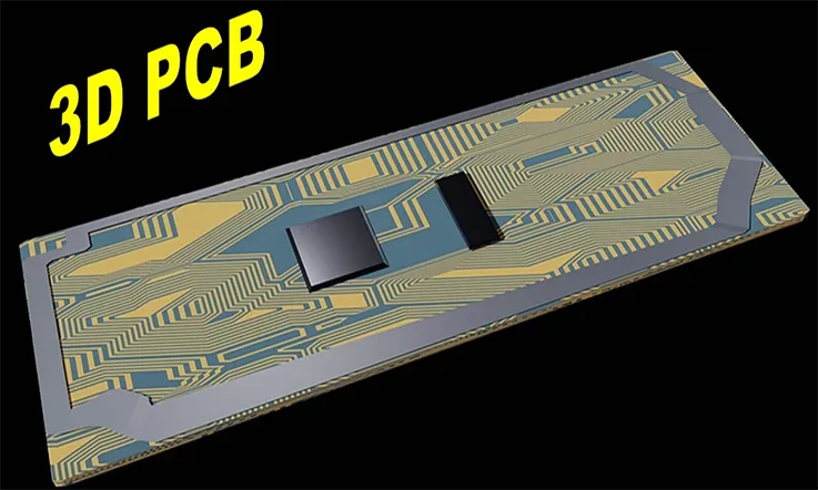
Method 4: Rapid Prototyping Techniques: Speeding Up Your Development
Rapid prototyping is the name of the game when it comes to speeding up the design and testing phases of PCB development. It’s like having a magic wand that lets you whip up prototypes in a flash, allowing for quick iterations and adjustments.
Key Rapid Prototyping Techniques
There are several techniques you can use for rapid prototyping, including:
● 3D Printing: Not just for plastic models anymore! Some advanced 3D printers can create PCBs with conductive materials.
● CNC Machining: This method involves using computer-controlled tools to carve out PCBs from larger blocks of material.
● Laser Cutting: This technique uses laser technology to cut and etch PCBs with high precision.
Please find the following cost Comparison and breakdown:
| Method | Cost | Time Required | Complexity |
| 3D Printing | Moderate | Moderate to Fast | Moderate |
| CNC Machining | High | Moderate | High |
| Laser Cutting | High | Fast | Moderate to High |
Implementing Rapid Prototyping in Your Workflow
1)Determine Your Needs: Identify what aspects of your PCB need rapid prototyping and choose the technique that fits best.
2)Select a Service Provider: Choose a service that specializes in rapid prototyping for PCBs.
3)Send Your Design: Provide your design files to the service provider and discuss your requirements.
4)Review Prototypes: Once you receive the prototypes, test them thoroughly and gather feedback.
5)Iterate: Use the feedback to make necessary adjustments, and repeat the prototyping process as needed.
Benefits and Challenges of Rapid Prototyping
Benefits:
● Speed: Quickly generate prototypes to test ideas and concepts.
● Flexibility: Easily make changes based on testing results.
● Cost-effective for iterations: While initial costs may be higher, rapid prototyping can save money in the long run by reducing the number of failed designs.
Challenges:
● Initial investment: The upfront costs for rapid prototyping equipment can be steep.
● Material limitations: Some rapid prototyping techniques may not offer the same durability as traditional methods.
● Learning curve: Mastering rapid prototyping techniques can take time and practice.
Cost Comparison and Breakdown
Here’s a comparison table analyzing the four PCB prototyping methods based on cost, advantages, and disadvantages:
| Method | Cost | Advantages | Disadvantages |
| DIY PCB Fabrication | Low to Moderate | Full control, cost-effective for small batches, educational experience | Time-consuming, requires skills and tools, high chance of errors |
| PCB Design Software | Varies (Free to High) | High precision, easy modifications, access to simulations | Steep learning curve, expensive software options, reliant on technology |
| Outsourcing | High | Expertise from professionals, time-saving, scalable for larger production | Less control, expensive for small runs, possible communication issues |
| Rapid Prototyping | Moderate to High | Quick iteration, flexible design changes, good for quick testing | High initial investment, material limitations, steep learning curve depending on technique |
This table organizes each method’s cost-effectiveness and key pros and cons, helping you decide which approach suits your needs.
How Many Methods testing for Your PCB Prototype?
Testing is the unsung hero of any successful PCB prototype. Whether it’s checking the electrical performance or running environmental tests, testing your prototype ensures your design doesn’t just look good on paper but performs well in real life. Functional testing will tell you if your design works as intended, while stress testing ensures the board holds up under extreme conditions. This is where you catch the bugs and optimize your design before committing to full production.
Key PCB Testing Methods?
1)Functional Testing: Ensure the board operates as expected in the real world.
2)Electrical Testing: Test signal integrity and voltage levels.
3)Environmental Testing: Expose the prototype to extreme conditions like heat and humidity.
Why Testing Benefits PCB Buyers?
1)Quality Assurance: Testing proves that the design meets the buyer’s expectations.
2)Cost Savings: Catching errors early prevents costly production mistakes.
3)Design Refinement: Testing allows for iterative improvements before final production.
Final Word
Prototyping is where your PCB design ideas become tangible, and the method you choose makes a big difference in how smoothly your project will go. Whether you choose to get your hands dirty with DIY fabrication, harness the power of design software, outsource to the pros, or jump into rapid prototyping, each method offers unique benefits tailored to different needs. And don’t forget—testing is your safety net, ensuring your prototype is ready to shine before you commit to production. Whatever you’re working on, choosing the right method for your needs is the first step toward PCB success. Time to roll up your sleeves and get prototyping!
So, whether you’re whipping up a prototype in your garage or overseeing a large-scale production run, remember that effective PCB prototyping is the key to turning your innovative ideas into reality. Now, go ahead and unleash your creativity—who knows what amazing electronic devices you’ll create next?
If you found this guide helpful, feel free to share your experiences or questions in the comments below. Whether you’re a seasoned pro or just starting out, we’d love to hear from you!
FAQs: Common Questions About PCB Prototyping Methods
How do I choose the best PCB prototyping method for my project?
Consider factors such as cost, precision, and time. If you need high precision and are working with complex designs, CNC or laser cutting may be best.
How Do I Test My PCB Prototype Effectively?
Testing is your best friend when it comes to prototyping. Start with functional testing to ensure your board operates as expected. Follow this up with electrical tests to check for signal integrity and voltage levels. If your board needs to withstand harsh conditions, environmental testing can reveal any weaknesses. These tests help fine-tune your design, ensuring you catch any issues before moving to full production.
How Do I Ensure My Prototype Matches My Design?
This is where Gerber files shine. These files ensure that every layer of your PCB—be it copper traces, solder mask, or silkscreen—is perfectly aligned with your design. The accuracy of Gerber files minimizes the chance of errors when your prototype is fabricated. It’s like handing over a blueprint to a builder and knowing they’ll create exactly what you envisioned.
Can I create multi-layer PCBs at home?
While possible, it’s much more difficult and typically requires advanced methods like CNC machining or laser cutting.
Is It Worth Testing Prototypes for Small-Scale Production?
100%! Even if you’re only producing a few units, testing your prototype can save you a ton of headache down the line. By catching errors early, you prevent the costly mistake of producing flawed boards. Plus, testing helps refine your design, so whether you’re making 10 boards or 1,000, the final product will perform as expected.
What’s the Long-Term Benefit of Choosing the Right Prototyping Method?
Choosing the right method isn’t just about making the prototype—it’s about ensuring a smoother production process down the road. By aligning your prototyping strategy with your final production method, you save time, money, and effort. The more aligned your prototype is with your final design, the fewer hiccups you’ll face when it’s time to scale up production.
Related Posts:
● Definition of Prototype PCB Service and Benefits
● Comprehensive PCB Prototype Services
● How to Manufacturing a Prototype PCB Circuit Board?