
If you’re stepping into the world of printed circuit boards (PCBs), you’ve probably heard how making a prototype PCB is like taking your ideas from paper to reality. But it’s not just about slapping a few copper traces together. This process is a delicate balance of design, materials, manufacturing steps, and, of course, testing.
In this guide, we’ll take you through the step-by-step process of manufacturing a prototype PCB circuit board, covering the ins and outs while also helping you avoid common pitfalls. We’ll also break it down into bite-sized pieces, so whether you’re a rookie engineer, an electronics manufacturer, or a seasoned buyer, you’ll be right at home here.
What is a Prototype PCB?
Before we dive head-first into the process, let’s make sure we’re all on the same page about what exactly a prototype PCB is. A prototype PCB is essentially the “first draft” of your electronic circuit board. It’s a way to validate your design, catch any errors, and fine-tune your product before committing to large-scale production.
Definition of a Prototype PCB
Simply put, a PCB prototype is the preliminary version of your printed circuit board, used to test whether your design works as intended. Think of it as the “test drive” before you take your design to mass production.
Key Differences Between Prototype PCBs and Production PCBs
While prototype PCBs and production PCBs might look the same at first glance, they serve different purposes. Prototype PCBs are all about design verification and ironing out the kinks, while production PCBs focus on efficiency, cost, and scalability. Prototypes might cost a little more per board and have a faster turnaround time, but that’s because they’re used to test and tweak things before you go all-in with full-scale manufacturing.
Why Use a Prototype PCB?
You might be wondering, “Why bother with a prototype?” Well, buddy, skipping this step is like going on a cross-country road trip without checking your gas tank. It could end in disaster. Prototyping helps ensure your PCB design is bulletproof before you pour money into production.
Advantages of PCB Prototyping in Product Development
Prototyping isn’t just a “nice-to-have.” It’s essential if you want to avoid costly mistakes down the road. A PCB prototype allows you to test everything—from the design to material selection—before scaling up. Imagine catching a flaw in your design after you’ve already made 10,000 boards. Not a pretty sight.
How Prototyping Helps in Design Verification?
At its core, prototyping is all about design verification. It’s your safety net, ensuring that what looks great on your CAD software works just as well in real life. Think of it as your chance to catch those “gotchas” before they bite you in production. Testing your PCB prototype will highlight any issues with layout, signal integrity, or material choice.
Step-by-Step Guide to Manufacturing a Prototype PCB Circuit Board
Let’s get down to the nitty-gritty of how you actually manufacture a prototype PCB. We’ll walk you through each phase, from design to testing, so you can start turning those dreams into copper and fiberglass reality.
Step 1: Designing the PCB Layout
Your PCB design is where it all starts. This is the blueprint for everything that follows. You’ll use a PCB design software to map out where every trace, via, and component will go. Make sure you’re thinking about factors like signal integrity, heat dissipation, and component placement. If you don’t get the design right, you’ll be in for a world of hurt later.
Best Practices for Designing a PCB Prototype Layout
While designing your PCB layout, keep things simple—especially for your first prototype. Focus on the essentials: clearances, trace widths, and layer stack-up. Additionally, you’ll want to think ahead for design for manufacturability (DFM). Many common issues arise during production, like solder mask alignment, via placement, and trace density, which can all be avoided by adhering to DFM guidelines from the beginning.
Considering Signal Integrity in PCB Layouts
In more complex or high-speed digital designs, signal integrity becomes a critical factor. To ensure optimal performance, it’s crucial to consider trace impedance, length matching, and return paths in your design. For RF or high-speed circuits, controlled impedance is a must, and this involves carefully selecting the trace width, layer stack-up, and dielectric material to meet the required signal performance.
Step 2: Material Selection for PCB Prototyping
Choosing the right materials can make or break your PCB prototype. For a prototype, you’re likely looking at FR4, the most common base material, but you might also consider materials like high Tg laminates if your application involves high heat. The key is to balance performance with cost since you’re not producing these boards at scale just yet.
Factors to Consider When Choosing PCB Materials
The material you choose will affect everything from thermal performance to signal speed. For a high-speed digital circuit, you might need a low-loss material like Rogers 4000 series, which offers a lower dielectric constant and dielectric loss than traditional FR4. For power electronics, thermal management could be your primary concern, requiring you to use a metal-core PCB to dissipate heat effectively.
In addition, applications like automotive, aerospace, and military electronics often demand high Tg materials (greater than 170°C) due to their ability to withstand elevated temperatures without deforming. Choosing a material that’s appropriate for the intended operational environment is vital for prototype accuracy.
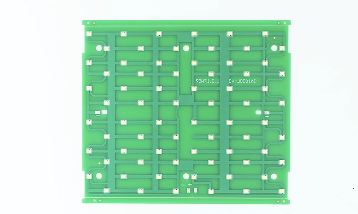
Step 3: Creating the PCB Stack-Up
The stack-up is like the sandwich of your PCB—it dictates the number of layers and how they interact with each other. A good PCB stack-up can minimize electromagnetic interference (EMI) and improve signal integrity, which is critical for high-speed circuits.
Optimizing the PCB Stack-Up for Prototyping
For prototypes, the stack-up should be simple yet effective. A 4-layer stack-up is common for many designs, but if you’re dealing with more complex circuits, you might need to go up to 6 or 8 layers. In more advanced designs, high-density interconnect (HDI) techniques, such as blind and buried vias, can be used to reduce the size of the PCB while maintaining electrical performance.
Using a well-optimized stack-up with ground planes and power planes adjacent to signal layers can reduce noise and improve signal transmission, making your prototype perform more like the final product.
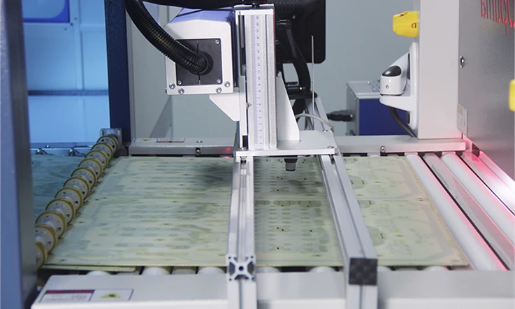
Step 4: Manufacturing the Prototype PCB
Now that your design is locked and your materials are chosen, it’s time to get down to manufacturing. This phase is where your design becomes a physical object. A lot of people choose quick-turn PCB manufacturers for prototyping to speed things up.
Choosing a Manufacturer for PCB Prototyping
When selecting a PCB manufacturer, it’s essential to prioritize those with a solid reputation in prototyping. Look for manufacturers that offer quick-turn services, high-quality standards, and advanced testing methods like AOI (automated optical inspection) and X-ray testing. It’s also helpful to work with manufacturers who provide DFM feedback, allowing you to catch potential manufacturability issues early in the process.
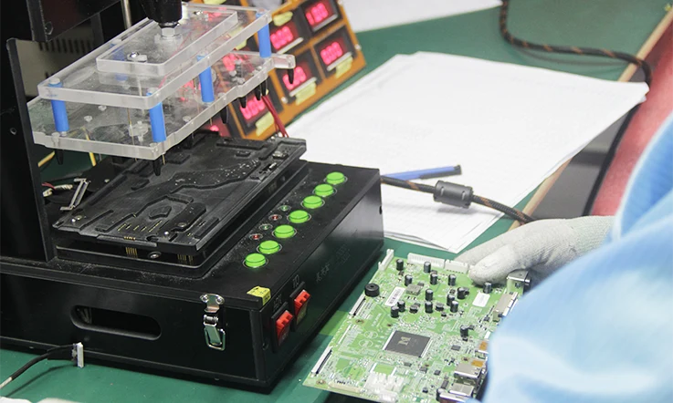
Step 5: Testing and Verifying the Prototype PCB
Testing is where you separate the winners from the duds. Once your prototype PCB is in hand, you’ll need to run it through a battery of tests to ensure it performs as expected. This is where you’ll discover any design flaws or manufacturing defects that could cause problems later on.
Common Tests for PCB Prototypes
Thorough testing is essential for any PCB prototype. Start with continuity tests and short circuit tests to ensure there are no open or shorted connections on the board. Beyond that, more advanced testing like signal integrity testing, thermal cycling, and environmental stress screening (ESS) will help you catch hidden issues.
Flying probe testing and in-circuit testing (ICT) are widely used in prototyping to ensure that each circuit is functioning correctly. For more complex designs, boundary scan testing can be employed to check for faults in digital logic and interconnects. These tests are critical if your board is going into production for high-reliability industries like medical or aerospace.
Ready to take your first PCB design from concept to reality? Get in touch with a trusted PCB prototype manufacturer(JarnisTech) and watch your vision come to life in just days. Whether you need a quick turn or a more complex design, there’s a solution waiting for you.
Fast Turnaround Time: How to Expedite PCB Prototyping?
We get it—when you’re developing a product, time is money. Fast turnaround on your PCB prototypes can be the difference between hitting the market first or getting stuck in development hell.
Key Strategies to Speed Up PCB Manufacturing
If you’re in a hurry (and who isn’t these days?), there are a few tricks you can use to speed up the process. First, simplify your design. The fewer layers and the less complexity you have, the faster your manufacturer can churn out your boards. Second, go with a quick-turn PCB manufacturer. Some manufacturers specialize in fast turnaround times, with the ability to deliver a prototype PCB in as little as 24 hours. Just keep in mind, the faster you want it, the higher the price tag.
Another way to expedite the process is to ensure your Gerber files and Bill of Materials (BOM) are error-free and complete before sending them to your manufacturer. This minimizes the back-and-forth and keeps your project moving forward.
Cost and Turnaround Time Estimates for Different PCB Prototype Types
| PCB Type | Layer Count | Material | Turnaround Time | Cost Range (USD) |
| Simple 2-Layer PCB | 2 | FR4 | 24-48 hours | $50 – $100 |
| Multi-Layer PCB | 4-6 | FR4 or Rogers | 3-5 days | $150 – $300 |
| High-Tg Prototype | 4-8 | High Tg FR4 | 5-7 days | $250 – $500 |
| HDI PCB | 8+ | Polyimide/Rogers | 7-10 days | $500+ |
| Quick-Turn PCB | 2-6 | FR4 | 24-48 hours | $100 – $400 |
Cost Considerations in Prototype PCB Manufacturing
Let’s talk dollars and cents—how much does it cost to manufacture a prototype PCB? The answer depends on several factors, including layer count, materials, and turnaround time. While you might pay as little as $50 for a basic two-layer prototype, a more complex design with multiple layers or specific materials could cost you several hundred dollars or more.
Factors Affecting Prototype PCB Costs
1)Layer Count: More layers mean more complexity, which translates into higher manufacturing costs. A simple 2-layer PCB will be much cheaper than an 8-layer HDI board.
2)Turnaround Time: As mentioned, fast production times come with a price. If you need your boards tomorrow, expect to pay a premium.
3)Materials: Standard FR4 is generally the cheapest option, but if your design requires higher thermal performance or low-loss materials like Rogers or polyimide, the price goes up.
4)Surface Finish: The type of surface finish you choose also plays a role in cost. HASL (Hot Air Solder Leveling) is the most affordable, but if your design demands better corrosion resistance or planarity, you might opt for ENIG (Electroless Nickel Immersion Gold), which is pricier.
Balancing Quality with Cost in Prototype PCBs
While it might be tempting to go for the cheapest option, remember that quality is key in prototypes. A low-cost board that fails in testing could end up costing you more in the long run. Choose a manufacturer that balances cost with quality, and always read reviews or ask for customer testimonials. Many manufacturers also offer DFM checks to catch potential manufacturability issues early, saving you time and money.
Don’t let cost hold you back from innovation. Compare prices and services from top PCB manufacturers to find a solution that fits your budget and timeline. Request a quote today and get started on your prototype journey.
Real-World Applications and Case Studies
Let’s look at a real-world example to highlight the importance of PCB prototyping. A team working on a next-generation automotive sensor module needed to validate their design under harsh conditions. They chose a 4-layer PCB prototype with high Tg materials due to the expected thermal stress in the final product.
During environmental testing, they discovered that the initial design had a heat dissipation issue that could have caused component failure in the field. By catching this during the prototype stage, they were able to revise the design, add thermal vias, and solve the problem before full-scale production.
This example highlights the critical role that PCB prototyping plays in product development. Prototyping allows you to test your design in the real world, catch issues early, and ensure that the final product is reliable and ready for market.
Advanced Testing Procedures for PCB Prototypes
Once your prototype is manufactured, the real work begins—testing. Proper testing ensures that your board functions as expected and meets all performance requirements. There are several tests you can run on your prototype PCB, ranging from basic electrical tests to more advanced reliability assessments.
Electrical Testing
One of the first tests you’ll run is an electrical test to verify that all connections are functioning correctly. This typically includes:
●Continuity testing to ensure all intended connections are made.
●Short circuit testing to verify there are no unintended connections between traces or pads.
Signal Integrity and Impedance Testing
For high-speed or RF applications, testing signal integrity and impedance is crucial. This ensures that your signals are transmitted cleanly and without interference, which is especially important for multi-layer PCBs and HDI boards. Improper impedance matching can cause signal degradation, timing issues, and crosstalk, leading to poor performance.
Thermal Shock and Environmental Stress Screening (ESS)
If your PCB will be used in extreme environments—whether it’s in the cockpit of a jet or the engine bay of a car—you’ll need to run thermal shock tests and environmental stress screening (ESS). These tests simulate rapid temperature changes and environmental conditions to ensure that your prototype can withstand the demands of its intended application.
Flying Probe and In-Circuit Testing (ICT)
In more complex designs, using flying probe testing or in-circuit testing (ICT) allows you to check individual components and circuit functionality. Flying probe tests each point of the board without requiring a custom fixture, making it ideal for prototypes. ICT, on the other hand, verifies that each component on the PCB is correctly placed and functional, detecting manufacturing errors like misaligned components or poor solder joints.
Boundary Scan and JTAG Testing
For digital circuit designs, boundary scan testing using JTAG protocols can help identify faults at the chip-to-chip interface level. This is particularly useful in complex multi-layer prototypes with tight signal routing, where physical testing would be impractical or impossible.
Testing is critical to success. Ensure your prototype PCB meets all performance standards with rigorous testing procedures. Reach out to expert manufacturers-JarnisTech, we can help you with everything from electrical testing to thermal shock simulations.
How to Choose the Right PCB Manufacturer for Prototyping?
Selecting the right PCB manufacturer is a critical step in the prototyping process. You want someone who can deliver high-quality boards quickly and at a reasonable price, but also someone who understands the complexities of your design and can provide valuable feedback during the manufacturing process.
What to Look for in a Prototype PCB Manufacturer?
Here are a few key things to consider when choosing a PCB manufacturer for your prototype:
●Quick Turnaround Times: Look for manufacturers that specialize in quick-turn services. Some companies can produce a prototype in as little as 24 hours, depending on the complexity of your design.
●Experience with Advanced PCBs: If your design includes HDI, controlled impedance, or high Tg materials, make sure your manufacturer has experience with these technologies.
●Quality Standards and Certifications: Make sure your manufacturer complies with industry standards such as ISO9001, IPC-A-600, and UL certifications. This ensures that your prototype will meet reliability and safety standards.
●Customer Support and DFM Feedback: A manufacturer that provides Design for Manufacturability (DFM) feedback is worth its weight in gold. DFM checks help catch issues early in the process, saving you time and money in the long run.
Wrapping Up
Making the Most of Your PCB Prototype
The journey from concept to PCB prototype is full of challenges, but the rewards are more than worth it. By following a structured approach, carefully selecting materials, optimizing your PCB design, and working with a reliable manufacturer, you can turn your prototype into a functional, market-ready product.
Testing is key—don’t rush through this phase. Each test gives you valuable insight into your design and can help you avoid costly mistakes during full-scale production. With the right balance of quality, speed, and cost-effectiveness, your prototype PCB will lay the foundation for a successful product.
And remember—prototyping isn’t just about catching errors; it’s about refining your design and ensuring it meets the needs of your target market. Whether you’re developing the next big consumer gadget or a mission-critical component for aerospace, your PCB prototype is where the magic begins.
Your next big breakthrough starts with the right prototype PCB. Partner with experienced manufacturers- JarnisTech who understand your needs and can help you navigate every step of the process. Contact us today to bring your design to life!
Frequently Asked Questions
1. What’s the difference between a prototype PCB and a production PCB?
A prototype PCB is primarily used to test and validate a design before full-scale production. It allows engineers to identify issues, make adjustments, and ensure that the final product will function as intended. Production PCBs, on the other hand, are built in large volumes and are ready for use in end products.
2. How long does it take to manufacture a prototype PCB?
The turnaround time for a prototype PCB depends on its complexity, the manufacturer’s capabilities, and your urgency. Quick-turn PCBs can be produced in as little as 24 hours, while more complex designs may take several days to weeks.
3. How much does a prototype PCB cost?
Costs vary widely based on factors such as layer count, materials, size, and turnaround time. Simple two-layer PCBs can cost as little as $50, but complex designs with more layers or specific material requirements may cost several hundred dollars or more.
4. Can I use the same design files for both prototype and production PCBs?
In most cases, yes. However, you should ensure that your design is optimized for mass production by considering DFM (Design for Manufacturability). Some design features that work in a prototype may not be feasible or cost-effective for mass production.
5. What materials are commonly used in prototype PCBs?
The most common material is FR4, but high-performance designs might require materials like polyimide or Rogers for better thermal or electrical performance. The choice of materials depends on the specific needs of the application, such as high-frequency or high-temperature environments.


