
In today’s advanced technological landscape, the incorporation of intricate and complex circuitry is becoming increasingly prevalent in high-tech devices. Accommodating these complex circuits poses a challenging task, often necessitating the addition of layers to the PCB stackup. This approach enables the realization of sophisticated electronic designs with improved functionality and performance.
The demand for higher layer counts, such as the 12-layer PCB stackup, arises from the need to address these complexities effectively. By employing a 12-layer stackup, designers gain the necessary flexibility to route signals, establish power and ground planes, and achieve optimal signal integrity. Moreover, the use of additional layers facilitates enhanced power distribution and mitigates issues related to crosstalk, thereby ensuring the reliable operation of modern automotive electronic devices.
In addition to meeting design requirements, controlling the thickness, durability, and overall production quality of the PCB is of paramount importance. A 12-layer PCB stackup enables manufacturers to exert precise control over these critical factors, ensuring the production of high-quality and reliable PCBs suitable for automotive applications.
To provide comprehensive insights into the 12-layer PCB stackup, we have compiled a FAQ guide below. This guide aims to address common inquiries and shed light on the intricacies associated with this advanced PCB configuration. Let’s delve into the guide and expand your knowledge on the subject.
What is a 12 Layer PCB Stackup?
The configuration of a 12 layer PCB stackup is essential for meeting specific requirements related to material thickness and trace heights in the manufacturing of multilayer printed circuit boards. This stackup arrangement enables the efficient organization of various circuit layers onto a single board, facilitating the design of complex circuits.
The design of a 12 layer PCB involves two crucial materials: thickness and prepreg. The prepreg consists of resin-treated glass, which serves the purpose of filling gaps between foils and acts as a core material for external layers, apart from the bonding layers. When designing the outermost layer, it is recommended to utilize copper foils with different weights, preferably no less than 0.5 ounces.
Typically, 12 layer PCBs are efficiently manufactured using boards with a thickness of 1.6mm. Moreover, these thicker boards can accommodate the fabrication of additional layers, ranging from 14 to 16 layers. The actual number of boards produced depends on the capabilities of the manufacturers specializing in high-density interconnect (HDI) boards.
By adhering to these considerations and employing proper stackup techniques, PCB engineers can ensure the successful realization of 12 layer PCBs, meeting the desired specifications and enabling the implementation of complex circuit designs.
Why is 12 Layer PCB Stackup Widely Used?
The use of a 12-layer PCB stackup has gained widespread popularity due to several key reasons:
1.Increased Design Flexibility:
The additional layers in a 12-layer PCB stackup offer designers greater flexibility in routing signals, power distribution, and ground planes. This flexibility is crucial for accommodating complex circuitry found in modern high-tech devices. It allows for efficient signal routing, reducing crosstalk and ensuring optimal signal integrity. The ability to allocate dedicated layers for power and ground planes also enhances noise reduction and power integrity.
2.High-Density Component Placement:
With the growing miniaturization of electronic components, high-density component placement has become a necessity. The 12-layer stackup provides more space for component routing, allowing designers to densely pack components on the PCB without compromising electrical performance. This is particularly important in automotive electronic devices where space is often limited.
3.Improved Signal Integrity:
Signal integrity is critical for reliable operation in high-speed and high-frequency applications. The use of additional layers in a 12-layer PCB stackup helps to minimize signal interference, impedance mismatches, and signal skew. By carefully controlling the layer stackup and utilizing dedicated signal layers, designers can achieve better control over impedance and optimize signal integrity.
4.Enhanced Power Distribution:
Efficient power distribution is essential for stable and reliable operation of electronic devices. The 12-layer stackup enables the allocation of multiple power and ground planes throughout the PCB, reducing voltage drops and improving power integrity. This is particularly important in automotive applications where power requirements can be demanding.
5.EMI/EMC Considerations:
Electromagnetic interference (EMI) and electromagnetic compatibility (EMC) are critical factors in modern electronic designs. The additional layers in a 12-layer PCB stackup provide better isolation and shielding, minimizing the potential for EMI and ensuring compliance with EMC standards. This is especially crucial in automotive electronics, where the presence of various electronic systems in close proximity can result in electromagnetic interference.
Despite the advantages, it is important to note that the decision to use a 12-layer PCB stackup should consider factors such as cost, manufacturing complexity, and the specific requirements of the design. However, the increasing complexity of electronic devices and the need for high-performance solutions have made the 12-layer PCB stackup a widely adopted choice in many industries, including automotive electronics.
What Are the Challenges of Designing 12 layer PCB Stack-up?
Designing a 12-layer PCB stackup presents several challenges that designers need to address to ensure successful implementation. Here are some of the key challenges associated with designing a 12-layer PCB stackup:
1.Signal Integrity:
Managing signal integrity becomes more complex with a higher layer count. Designers must carefully consider factors such as impedance control, signal routing, and length matching to mitigate signal integrity issues, such as signal reflections, crosstalk, and timing skew.
2.Power and Ground Plane Distribution:
Allocating power and ground planes across multiple layers in a 12-layer stackup requires careful planning and consideration. Designers must ensure proper power distribution and minimize voltage drops while maintaining low impedance paths for return currents. This involves designing appropriate power and ground plane structures and optimizing via placement.
3.Layer Stacking and Signal Routing:
Determining the arrangement of layers in the stackup and efficiently routing signals across multiple layers is a critical challenge. Designers need to consider factors such as signal density, high-speed signal paths, and thermal management. Careful layer stacking and signal routing techniques, including the use of blind and buried vias, are necessary to optimize performance and minimize signal interference.
4.Manufacturing Complexity:
Increasing the layer count adds complexity to the manufacturing process. The fabrication of a 12-layer PCB requires precise alignment and registration of the multiple layers, which can be challenging. Manufacturing processes, such as layer lamination, drilling, and plating, need to be meticulously controlled to ensure the desired layer stackup and minimize manufacturing defects.
5.Cost Considerations:
Designing and manufacturing a 12-layer PCB stackup typically incurs higher costs compared to lower layer counts. The additional layers, increased complexity, and more stringent manufacturing requirements contribute to higher material and fabrication costs. Designers must carefully balance the benefits of a 12-layer stackup against the associated costs and the budget constraints of the project.
6.Design Rule Complexity:
With more layers, the design rule complexity increases. Designers need to be well-versed in the specific requirements and limitations of the fabrication process and PCB manufacturer to ensure that the design adheres to the necessary design rules and guidelines.
How Do You Plan a 12 Layer PCB Stack-up?
Planning a 12-layer PCB stackup involves a systematic approach to ensure optimal signal integrity, power distribution, and manufacturability. Here are the key steps involved in planning a 12-layer PCB stackup:
1. Determine Design Requirements: Understand the specific requirements of your PCB design, including factors such as signal integrity, power distribution, thermal management, and EMI/EMC considerations. Consider the electrical characteristics of the components, high-speed signal paths, and any specific design constraints.
2. Layer Allocation: Decide on the allocation of layers for various purposes such as signal routing, power planes, and ground planes. Typically, the inner layers are dedicated to power and ground planes, while the outer layers are used for signal routing.
3. Signal Layer Placement: Identify critical high-speed signal layers that require careful placement. These layers should be evenly distributed throughout the stackup to minimize signal interference and crosstalk. Consider grouping signal layers based on their speed and proximity to reduce the impact of electromagnetic coupling.
4. Power and Ground Plane Distribution: Determine the number and placement of power and ground planes. Ensure that there are sufficient power and ground planes to meet the power requirements of the design and minimize voltage drops. Consider splitting power planes to separate sensitive analog and digital components and minimize noise coupling.
5. Impedance Control: Analyze the impedance requirements of high-speed transmission lines and ensure that the stackup provides controlled impedance throughout the PCB. This involves selecting appropriate dielectric materials and layer thicknesses and calculating trace widths and spacing.
6. Via Planning: Plan the placement of vias for signal, power, and ground connections. Determine the via types, such as through-hole vias, blind vias, or buried vias, based on the design requirements. Optimize via placement to minimize signal reflections, maintain impedance control, and reduce the complexity of signal routing.
7. Thermal Considerations: Consider thermal management by strategically placing thermal vias and allocating internal copper planes for heat dissipation. Ensure that the heat generated by components can be efficiently dissipated through the stackup to prevent overheating and ensure reliable operation.
8. Design Rule Check (DRC): Perform a thorough design rule check to verify that the planned stackup adheres to the manufacturer’s capabilities and design guidelines. Ensure that the design meets minimum trace and spacing requirements, via aspect ratios, and other manufacturing constraints.
9.Collaboration with PCB Manufacturer: Consult with your chosen PCB manufacturer to review the planned stackup and ensure its manufacturability. Discuss any specific manufacturing requirements, such as layer registration tolerances, material availability, and fabrication processes.
How Can You Design a 12 Layer PCB Stackup?
Designing a meticulous 12-layer PCB stackup is of paramount importance when dealing with high-speed circuits. PCB design is akin to an art form for developers, as a poorly designed printed circuit board can significantly hinder electrical performance, including power delivery, signal transmission, producibility, and overall appliance reliability.
In the current PCB market, the adoption of flexible, cost-effective, and multilayer PCBs is on the rise, making the utilization of a 12-layer stackup an optimal choice. This configuration provides designers with the necessary capabilities to meet the evolving demands of modern electronic applications.
When embarking on the design of a 12-layer PCB stackup, it is crucial to gather all the essential documents required for PCB board assembly. These vital files include the Bill of Materials (BOM), pick and place file, PCB Gerber file, and silkscreen file. Among them, the BOM file holds particular significance.
The BOM file serves the purpose of streamlining the PCB assembly process by providing accurate component information, ultimately allowing the PCB assembly company to generate precise quotations and facilitating more efficient PCB assembly workflows.
By focusing on creating a practical and comprehensive BOM file, designers can save valuable time during the PCB assembly stage and ensure the accuracy of component selection, leading to improved efficiency and reduced chances of errors.
Therefore, when striving for a flawless 12-layer PCB stackup design, meticulous attention should be given to generating a well-structured BOM file. This approach not only optimizes the PCB assembly process but also contributes to overall project success and customer satisfaction.
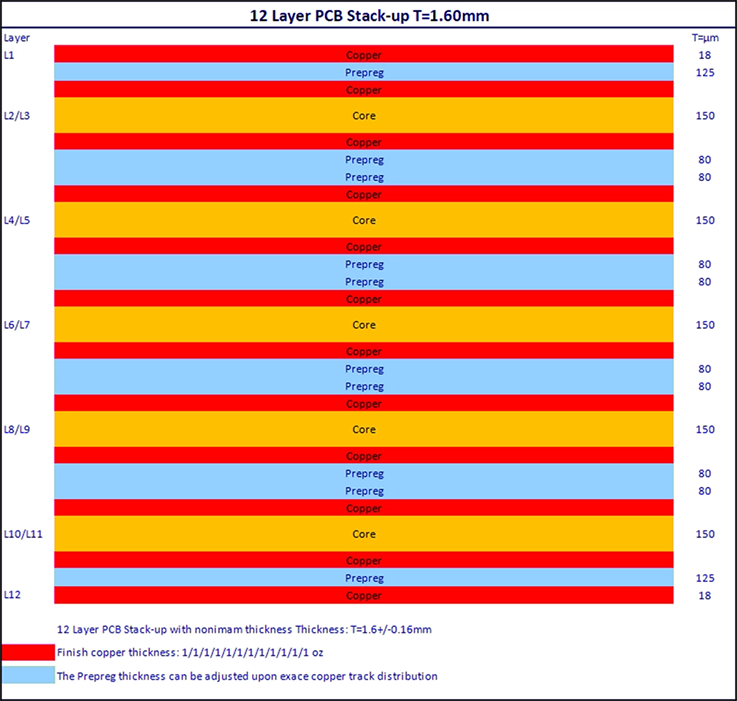
What is the Standard Thickness for a 12-layer PCB?
The typical thickness utilized for a 12-layer PCB is 1.6mm, which has become the prevalent choice within the industry. However, it is important to note that this value is not rigidly fixed and may vary depending on the specific requirements of the circuit design.
It is crucial to recognize that a standardized thickness may not be suitable for all types of circuits. Certain PCBs may necessitate thicker materials to fulfill specific objectives, such as enhancing mechanical robustness or achieving improved isolation between layers. These considerations are taken into account to ensure the optimal performance and reliability of the PCB in its intended application.
Difference Between 12-Layer and 8-Layer PCB Stackup
The difference between a 12-layer and 8-layer PCB stackup lies in the number of layers and their arrangement within the printed circuit board (PCB). Here’s a breakdown of the key distinctions:
1. Number of Layers:
12-layer PCB: A 12-layer PCB consists of twelve individual layers, each of which can be used to route signals or provide power and ground planes.
8-layer PCB: An 8-layer PCB, on the other hand, comprises eight individual layers.
2. Signal and Plane Distribution:
12-layer PCB: With more layers available, a 12-layer PCB offers greater flexibility in distributing signals and power/ground planes. This allows for improved signal integrity, reduced crosstalk, and better power distribution.
8-layer PCB: An 8-layer PCB has fewer layers, which means there are fewer options for signal routing and power/ground planes. Consequently, it may be more challenging to achieve optimal signal integrity and power distribution.
3. Complexity and Manufacturing:
12-layer PCB: Due to its greater layer count, a 12-layer PCB is typically more complex to design and manufacture. It requires advanced design techniques and manufacturing processes to ensure signal integrity and proper layer registration.
8-layer PCB: An 8-layer PCB is comparatively less complex to design and manufacture since it has fewer layers. It may be a more suitable choice for simpler electronic designs or applications with lower density and complexity.
4. Cost Considerations:
12-layer PCB: The additional layers and complexity of a 12-layer PCB generally result in higher manufacturing costs compared to an 8-layer PCB. The cost of materials, fabrication, and assembly may increase due to the increased layer count and associated design complexity.
8-layer PCB: An 8-layer PCB is typically more cost-effective to produce since it requires fewer layers and may involve simpler manufacturing processes.
The choice between a 12-layer and 8-layer PCB stackup depends on the specific requirements of the electronic design, including the complexity of the circuit, density of components, signal integrity considerations, and cost constraints. More complex designs with higher-speed signals and tight layout constraints may benefit from a 12-layer stackup, while simpler designs may be adequately served by an 8-layer stackup.
What Are Factors Affecting Cost of 12-Layer PCB Stackup?
Here are some of the key factors that can affect the cost of a 12-layer PCB stackup:
Material Quality: Higher-quality materials like high-frequency laminates are required for applications with stringent electrical performance needs. These specialist materials tend to be more expensive than standard FR-4.
Board Size: Larger board sizes translate to higher material usage and longer fabrication times. As such, a bigger board footprint will drive up costs compared to a smaller design.
Copper Weight: Applications involving high current carrying necessitate thicker inner copper layers. Increasing copper weights across 12 layers escalates material costs.
Thermal Properties: Higher glass transition temperature materials are needed when boards must withstand elevated operating temperatures. Custom resin formulations to boost thermal ratings command cost premiums.
Via Specifications: Denser via patterns or smaller diameter holes complicate the drill and plate processes. More conductive material is also used per board. Tighter via specs increase manufacturing overhead.
Custom Requirements: Non-standard specifications necessitating specialized tooling, equipment or labor increase per-unit fabrication expenses. Complex demands beyond routine production impact the bottom line.
Overall, choices affecting layer counts, conductor weights, thermal profiles, via implementations or unique design rules exert considerable influence on the total price of a multi-layer printed circuit board. Careful material selection and simplifying the form factor where feasible can help minimize costs.
Why Choose Us
JarnisTech – Leading 12 Layer PCB Supplier in China
JarnisTech is a leading PCB manufacturer with over 20 years of experience in designing and fabricating single-layer to advanced multi-layer boards. As a trusted partner to clients worldwide, we offer full-service capabilities including component sourcing, prototype development, assembly, testing and fulfillment.
Qualifications:
We have particular expertise in 12-layer PCB stackups, having delivered thousands of designs to strict tolerances on-time and on-budget. Our optimized manufacturing processes incorporate the latest materials and technological capabilities. All production is conducted in IPC-610 certified facilities and subject to rigorous quality inspections.
Commitment to Customers:
At JarnisTech, clients benefit from personalized attention, rapid turnarounds and responsive technical support from concept through mass production runs. Our manufacturing experts are available for consultation on stackup planning, lamination, drilling, routing and finishing to help achieve the best electrical and mechanical outcomes.
Scope of Services:
In addition to advanced PCB stacks, our facilities support the complete assembly spectrum from quick-turn prototypes to high-volume commercial runs. We maintain strategic supplier partnerships to ensure accessibility of worldwide component inventories. Comprehensive testing and logistics rounds out our value-added service portfolio.
In Summary
12-layer PCB stackups require meticulous planning and coordination between design and fabrication to achieve optimized electrical performance, thermal management, and manufacturability. Close cooperation is needed between engineers, material scientists and manufacturers during the development process. With a judicious balance of design optimization, cost control, and process control, the inherent complexities of 12-layer designs can be navigated to produce robust, feature-rich circuit boards.
Though demanding, multi-layer PCB technology plays a vital role in continuously advancing modern electronics. Through diligent consideration of the factors reviewed here, engineers can harness its capabilities to realize even the most sophisticated system-on-board aspirations.


