In modern times, electronic manufacturing companies are designing increasingly complex printed circuits with multiple layers, causing a surge in the importance of PCB stackup design. It is common knowledge that a well-designed stackup is crucial for reducing radiation from PCB loops and associated connections. Conversely, a poorly designed stackup can significantly increase radiation levels, posing potential safety hazards.
The growing demand for smaller electrical goods compels companies to use PCBs with multiple layers and a three-dimensional design approach, leading to new challenges in design tactics like SMD packaging and layer stackup. As printed circuits become ever more sophisticated, with a high number of layers, the stackup or stack of PCBs has gained increasing importance in design considerations. Compared to earlier times when PCB designs were rudimentary and only served as a platform for connecting electronic components, there was minimal need for multi-layer stacking due to the simplicity of these designs.
To create highly professional and reliable systems, it is essential for electronic manufacturers to consider specific guidelines while designing stacks. Let us delve into some of these crucial guiding principles.
Definition of PCB Layer Stackup
In the domain of PCB design, the term “Layer Stackup” refers to the arrangement and configuration of the conductive and insulating layers that make up a printed circuit board prior to final board design. A PCB layer stackup is a critical aspect of the overall design process, as it determines the electrical and mechanical properties of the board and affects its performance, impedance, and reliability. The proper layer stackup is essential for achieving optimal signal integrity, power distribution, and thermal management in any PCB design.
PCB Layer Stack-Up Basics
PCB layer stack-up basics include:
● There are typically two types of PCB layers: signal layers and power/ground planes. Signal layers carry electrical signals and are routed using traces. Power/ground planes provide a low-impedance path for the flow of current and help to reduce noise in the circuit.
● Inner Layers vs. Outer Layers: Inner layers are buried within the PCB and are not visible from the outside. Outer layers are visible and can be seen on the surface of the PCB.
● Copper Weight: The thickness or weight of the copper layer impacts the current carrying capacity and impedance of the PCB. The most common copper weights are 1 oz and 2 oz.
● Prepregs: Prepregs are layers of material that provide insulation between copper layers. They are made of resin and fiberglass, and the thickness impacts the overall thickness of the PCB.
● Impedance Control: Impedance control is important for ensuring consistent signal integrity. The distance between copper layers, copper thickness, dielectric constant of the substrate material, and trace geometry all impact impedance.
Main Advantages of Stack Up
● A well-planned PCB layer stackup can significantly reduce external interference, radiation, and impedance and crosstalk issues that may arise in high-speed PCB layouts. Moreover, with a proper layer stackup, you can strike a balance between low-cost efficient production processes and preserving signal integrity, which is imperative for high-performance electronic devices.
● By selecting the appropriate layer stackup, you can improve the Electromagnetic Compatibility (EMC) of your PCB design. Considering the advantages, pursuing a stacked PCB arrangement is often a practical and advantageous choice for applications based on printed circuit boards. Therefore, it is crucial to have a thorough understanding of PCB layer stackup design principles when creating complex PCB designs to achieve optimal performance and reliability.
General layers in multilayer PCBs include the ground plane (GND plane), power plane (PWR plane), and inner signal layers. An example of an 8-layer PCB stackup is shown below.
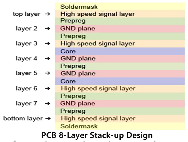
In PCB design, the distribution of layers in a printed circuit board follows a symmetrical or balanced structure, as depicted in the diagram. Alongside the layer distribution, it is also crucial to consider the spacing between layers. To achieve miniaturization goals, trace spacing must be minimized during the layer stack-up planning process. The interlayer space can comprise either core or prepreg materials. When fabricating multilayer PCBs, one or more cores and prepregs can be used.
The cores consist of copper-plated glass-reinforced epoxy laminate sheets, with thicknesses ranging from 0.1mm to 0.3mm. PCB design engineers must take into account these factors and carefully select core and prepreg materials with the appropriate thicknesses and interlayer spacing to improve signal integrity, reduce noise, and enhance various other PCB performance metrics. Proper layer stack-up planning is vital to ensure that the PCB is optimized for efficient signal transmission and high reliability.
PCB Stackup Design Rules and Considerations
The design and construction of a PCB layer stackup has a significant impact on the board’s production and assembly. During the fabrication process, it is crucial to consider key factors such as the number of layers and their layout, as well as the type of materials used. These considerations enable a balance between thickness constraints, material parameters such as coefficients of thermal expansion, dielectric constant, electrical strength, and signal isolation.
It’s important to carefully select the appropriate through-routing option, as it can impact the overall stackup design. PCB designers must be mindful of the various parameters that influence stackup design to ensure optimal performance and reliability. Understanding these factors is essential in creating an optimized PCB layer stackup, which can result in efficient signal transmission, while also limiting noise and EMI issues. Therefore, PCB designers must pay close attention to these aspects to create a highly-functioning printed circuit board.
● Number of Layers: When planning your printed circuit board (PCB) stackup, the first factor to consider is the required number of layers. This decision should be based on factors such as the type of signals (high-speed, low-speed), power demands (high-power boards or circuits utilizing power supplies), and ground layers or planes. It is strongly recommended to avoid mixing different types of signals on inner layers. For most boards, the layer count can be calculated using the pin density.
Once the pin density has been determined, it is advisable to consult your contract manufacturer (CM) for stackup support or refer to a readily available lookup table to determine the number of signal layers and the total number of layers required. Additional information, such as the values for controlling impedance, may also be required.
By thoroughly considering these factors and leveraging the expertise of your CM or utilizing reliable lookup tables, you can achieve a well-optimized PCB stackup that meets your design requirements and ensures optimal performance.
● The number of Signal Layers: In the design of printed circuit boards, the number of signal layers required can depend significantly on the intended application of the board. For example, high-speed signal or high-power applications often require more signal layers than low-speed signal applications.
When designing complex devices with a low pitch and a large number of pins, such as ball grid arrays (BGAs), it may be essential to use additional signal layers to accommodate the increased number of required connections.
Stringent signal integrity requirements, such as extremely low crosstalk, may also necessitate an increase in the number of signal layers to ensure optimal performance.
For mixed-signal applications, the separation of analog and digital signals is typically required, which often results in an increased number of signal layers.
During the design phase, the use of a signal and power layer estimation tool can be invaluable in determining the precise number of signal layers required to meet specific design requirements. By leveraging these tools, design engineers can allocate signal layers effectively and fine-tune their circuit board designs to optimize performance and functionality.
● The Number of Power and Ground Layers: Designers can employ ground and power planes to allocate certain signal layers exclusively for routing signals. These planes also help to minimize DC resistance in the power and ground rails, leading to a reduced DC voltage drop at the devices.
The ground layer refers to the copper plane connecting to the ground connector of the power supply. On the other hand, a power layer is a flat copper plane joined to the power supply rail.
Furthermore, these planes act as high-frequency and time-varying signal return pathways, reducing noise and signal crosstalk and promoting signal integrity. Power planes also improve the circuit’s capacitive decoupling capability, reduce electromagnetic radiation, and enhance electromagnetic compatibility (EMC) performance. By leveraging these benefits during the printed circuit board design process, designers can optimize the circuit’s reliability and performance.
● Controlled Impedance Traces: A controlled impedance trace is a circuit board trace and related planes that create the characteristic impedance of a transmission line. Achieving a uniformly managed impedance is crucial for preserving signal integrity.
In cases where the reference plane is not present on the adjacent layer, another copper feature located on that layer may serve as the reference.
During the manufacturing process, it is necessary to ensure a homogeneous etch across the length of the line, including the breadth and trapezoidal effect. To meet these requirements, etching tolerances must be maintained and consistency in the etching process is critical. By paying close attention to these details, designers can achieve optimal manufacturing outcomes, resulting in a printed circuit board design that performs efficiently and reliably.
● Spacing Between The Layers: In printed circuit board design, it is crucial to maintain a close coupling between the signal and current return planes to reduce capacitance. The coupling between ground and power planes should also be maintained at a close proximity.
Regardless of which adjacent plane they occupy, signal layers must always be situated near one another. Achieving tight coupling and a suitable layer spacing is necessary for ensuring continuous signaling and overall operational efficiency. It is advisable for designers to adhere to these principles during the layout to optimize the performance and functionality of the printed circuit board.
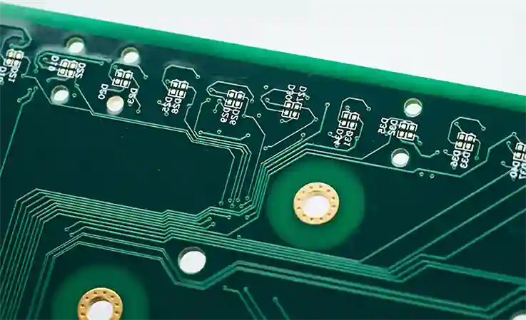
● Trace Width and Spacing: The routing of ball grid array (BGA) packages presents a significant challenge to PCB layout. During the design process, designers must pay close attention to the breakout area and determine the number of signals that require routing between vias. This crucial step establishes the minimum trace width and spacing that should be employed.
It is of vital importance to ensure that a minimum line width is observed to avoid any potential negative impacts on signal quality. PCB designers should carefully examine the design to check for any detrimental effects that may arise with narrow trace widths and make necessary adjustments. By following these guidelines, designers can effectively address challenges associated with routing BGA packages, thereby optimizing the design of the printed circuit board.
● Layer Arrangement: When designing a printed circuit board, determining the number of layers is a crucial first step. After that, it is necessary to establish how the layers should be stacked or ordered. Here are some good ground principles to follow:
● Route high-speed on minimum thickness microstrips.
● Avoid having two signal layers adjacent to each other.
● Place signal layers next to internal power layers for tight coupling.
● Make the stackup symmetric from the top and bottom layers inward.
● Power and ground layers should have minimal spacing between them.
When designing a printed circuit board, an essential aspect of stack-up architecture is the placement of sequential layers. Before routing, designers must carefully consider the arrangement of high-speed signal layers, with placement according to microstrip thickness being a crucial element. Signal layers are often situated close to the ground or power plane, leading to tight coupling.
In addition, limiting the number of lamination steps in sequential lamination plays a critical role due to the potential for increased costs and time consumption. PCB designers must maintain a good balance between stack-up complexity and cost-effectiveness to produce an optimal board design that meets performance, reliability, and fabrication requirements.
● Determining Layer Material Types: When designing a printed circuit board, selecting materials for the layer stackup is a critical aspect that requires consideration of their thermal, mechanical, and electrical properties, as well as how they interact with one another. For signals, 0.5-ounce copper is typically employed, while 1-ounce copper is used for power planes, and 2-ounces of copper may be used for high-current applications.
Typically, printed circuit boards feature a solid fiberglass substrate core that provides the PCB with thickness and strength. Some flexible PCBs, on the other hand, may use a flexible high-temperature plastic.
The next layer in the stackup consists of a thin copper foil that is affixed to the board. In double-sided PCBs, copper is found on both substrate sides, with the thickness of the copper varying depending on the layering of the PCB stack.
A solder mask layer is applied over the copper foil to prevent the copper traces from coming into contact with other metals. This layer is crucial in aiding users in soldering to the correct location while avoiding solder jumpers.
The silkscreen layer is applied over the solder mask layer to include symbols, numbers, and letters, making it easier for humans to understand the board and facilitate assembly. PCB designers must carefully select each of these components, ensuring they are sized appropriately and function optimally, for an optimized printed circuit board.
● Determining Routing and Vias: When designing a printed circuit board, it is important to route high-speed signals on intermediary layers located between levels. This design practice enables ground planes to act as a shield, effectively containing radiation produced by fast-moving signal tracks.
When signal levels are placed in proximity to plane levels, nearby planes are able to conduct the return current, reducing the return path inductance to a minimum. With standard construction techniques, it is possible to achieve decoupling below 500 MHz, thanks to the insufficient capacitance between adjacent power and ground planes.
High-speed signals are prone to signal integrity issues, and therefore, thorough consideration must be given to PCB design principles. By keeping these aspects in mind, designers can ensure effective signal transmission, reduce noise, and enhance the reliability and performance of printed circuit boards.
Recommendations in Design PCB stack-up
To achieve an optimal printed circuit board (PCB) stack-up design, several best practices should be followed. Firstly, it is recommended to limit the number of sequential layers to three or fewer to reduce processing time and keep costs and delivery times under control.
When using stacked vias, they should be filled after each sequential layer, which can add complexity to the manufacturing process and increase the build-up’s span. Therefore, using staggered vias can be a cost-effective alternative if the design permits.
It is crucial to know the specific layers in which mechanical buried vias will be implemented and to determine the need for staggered and buried vias. This information must be carefully considered during the stack-up design phase.
It is also worth noting that sequential lamination may not be suitable for all materials. As such, manufacturers should verify the suitability of their materials for sequential lamination during the planning stages to avoid any potential issues during manufacturing.
By following these guidelines, you can design a well-optimized PCB stack-up that is technically sound and exhibits excellent manufacturability, ensuring a successful outcome for your PCB project.
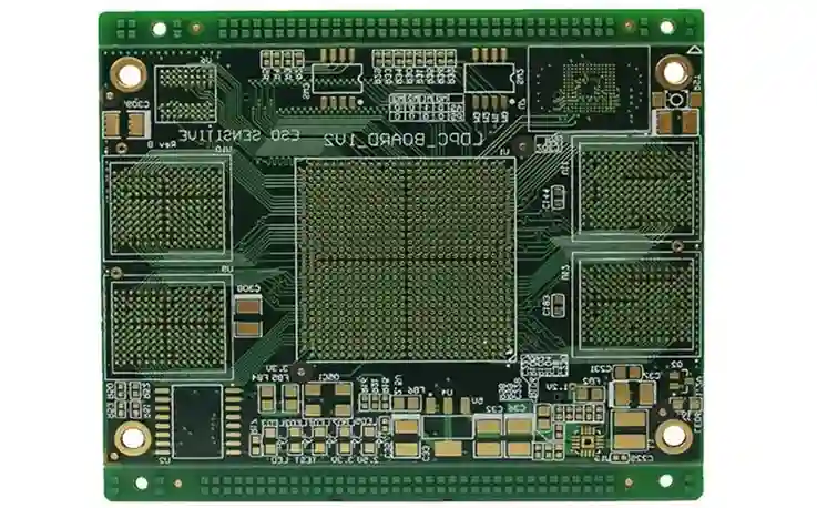
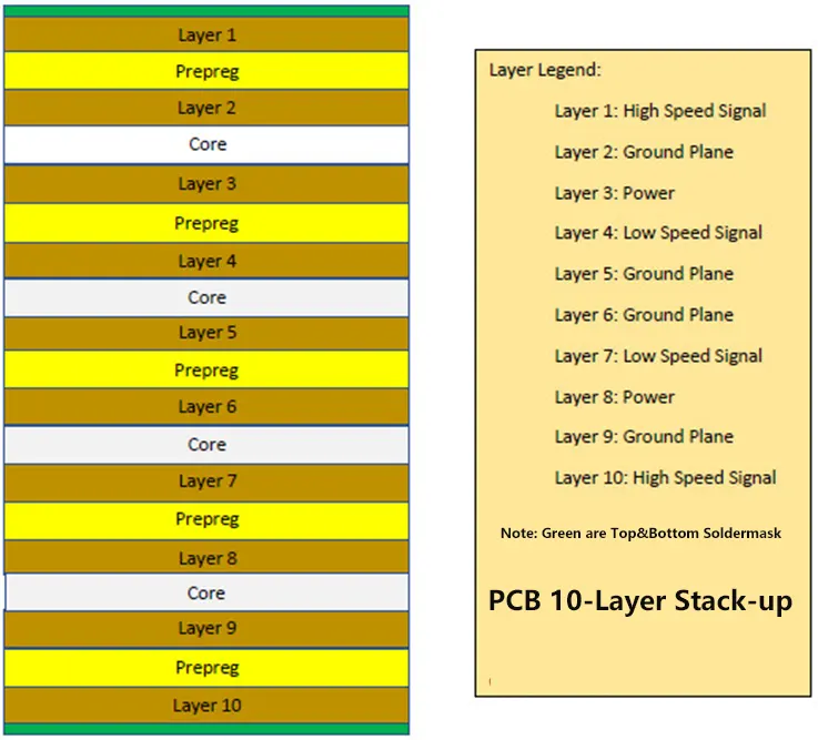
PCB Stackup Design Example
Several PCB stack-up options can be accomplished depending on how you apply the tips mentioned earlier. This reference graphic demonstrates an exemplary 10-layer PCB stack-up design that is particularly useful in PCB design projects.
In modern circuits with high operating speeds, effective PCB stack-up design is critical to optimize distribution capabilities while minimizing interference. Poorly designed PCBs can significantly impact signal transmission, manufacturability, power delivery, and long-term reliability.
Multilayer PCBs offer extensive opportunities for creativity and can fully realize the potential of electronic circuits. Therefore, it is wise to entrust the design process to reputable companies that specialize in producing high-quality electronic products.
By engaging reliable design companies, design engineers can be assured of technically sound PCB designs that meet their specific requirements, including optimized stack-up configurations that meet the needs of high-speed circuits. These design firms have the expertise and best practices necessary to produce PCBs that provide excellent manufacturability, functionality, and reliability over the product’s lifetime. Ultimately, this approach can lead to high-quality electronic products with excellent performance and longevity.
Common PCB Layer Stack-Up Configurations
There are several common PCB layer stack-up configurations, including:
● 2-Layer PCB Stack-Up: Consists of two layers of copper, separated by a substrate material. This is the simplest type of PCB and is often used for low-speed or low-complexity circuits.
● 4-Layer PCB Stack-Up: Consists of two internal signal layers and two power/ground planes, separated by substrate layers. This is a common layer stack-up for complex, high-speed PCBs.
● 6-Layer PCB Stack-Up: Consists of two internal signal layers, two power planes, and two ground planes, separated by substrate layers. This stack-up is commonly used for high-speed or mixed-signal PCBs.
● 8-Layer PCB Stack-Up: Consists of four internal signal layers and two power/ground planes, separated by substrate layers. This stack-up is commonly used for very complex, high-speed PCBs.
● 10-Layer PCB Stack-Up: Consists of six internal signal layers and two power/ground planes, separated by substrate layers. This stack-up is commonly used for extremely complex, high-speed PCBs with multiple high-speed interfaces.
The exact layer stack-up used for a PCB depends on the specific requirements of the circuit and the system it is a part of, as well as any manufacturing or cost considerations.
Summary
Careful PCB Design Is Important!
In today’s high-speed circuits, exceptional PCB design is essential and has become an art form in its own right. Poorly designed printed circuit boards can lead to decreased electrical performance with respect to signal transmission, power delivery, producibility, and long-term reliability, negatively affecting the final product.
Submission of Gerber files to PCB manufacturers establishes production costs, where the cost per unit progressively decreases with increasing quantity. The surge in the usage of multilayer and flexible PCBs is driving the global expansion of the PCB industry. As electronics companies try to add more functionality to their devices, board density and design complexity continue to increase. For most consumers, the most critical factors for selecting a PCB manufacturer are price, quality, delivery time, and service, with price often being the primary consideration.
At JarnisTech, we are committed to reducing lead times during the critical prototype phase. By providing fast quotes in just 10 minutes and delivery lead times as short as 5 working days, we offer our customers greater peace of mind when it comes to their PCB manufacturing and prototyping needs. Our goal is to empower our customers with high-quality, reliable, and timely PCB manufacturing services that meet their specific requirements and help them achieve their business goals.
Related Posts:
1.Why Need to Know 4 Layer PCB Stack-up Technology
2.The Complete Guide to 6 Layers PCB Stack-up
3.The Ultimate Guide of 8 Layer PCB Stackup
4.The Best 10 Layer PCB Stack-up technology Guide