
Universal PCB manufacturing focuses on adaptable circuit board platforms designed for low-volume, high-mix production. This guide provides a detailed look at each stage of the process—from fabrication and assembly to material selection, testing, and inspection.
It covers essential manufacturing steps like drilling, plating, soldering, and surface finishes, followed by assembly techniques like wave soldering and hand soldering. Material selection is explored through a comparison of FR-4, CEM-1, and ceramic substrates, with attention to thermal, electrical, and mechanical properties.
The guide also discusses stack-up design, signal integrity, and ground plane strategies for high-speed applications. For startups, it highlights BOM flexibility, rapid prototyping, and sourcing strategies. Thermal management and coatings are addressed to ensure long-term reliability.
What Is a Universal PCB?
If you’ve been involved in electronics for a while, you’ve likely come across Universal PCBs. These are not your standard, mass-produced circuit boards. Instead, they offer flexibility and adaptability that allow engineers to quickly and easily create prototypes or small-volume designs. A Universal PCB serves as a platform for experimenting with layout and component placement without committing to a specific, more complex configuration. From wearable devices to early-stage medical sensors, these boards provide the structural freedom required to streamline the development process.
In this section, let’s explore the details and functionality of Universal PCBs. We’ll break down how they are constructed, the various types available, and how they are used in different industries. By the end, you’ll have a solid understanding of how these boards can support your projects.
Understanding Universal PCB Architecture
A Universal PCB is often seen as a blank slate for circuit developers. It’s designed with a simple structure—essentially, it’s a board that has pre-drilled holes where components can be placed and connections manually routed. Unlike custom PCBs, which include predefined traces, the Universal PCB leaves the trace layout open for manual design and experimentation.
Most Universal PCBs follow a standard 2.54mm pitch for the holes, making them compatible with through-hole components such as resistors, capacitors, and header pins. While the simplicity of the design provides flexibility, it also means that the routing of electrical connections—using soldered wires, copper tape, or jumper wires—is left to the user handling the assembly and layout.
The architecture of Universal PCBs is built around providing flexibility and adaptability. Despite the open design, we must still pay attention to aspects like signal integrity, power handling, and heat dissipation, ensuring that the board can handle the requirements of their particular circuit without introducing issues down the road.
Common Types of Universal PCBs and Their Features
Let’s take a closer look at the various types of Universal PCBs you might encounter. Understanding these different formats will help you choose the most appropriate one for your needs.
Perfboard-
●Layout: Features individual copper pads for each hole, allowing you to place components freely.
●Use Case: Best for projects where flexibility in component placement is needed. Perfect for initial prototype circuits or testing where you might need to adjust the design frequently.
Stripboard-
●Layout: Copper strips that run along the length of the board with perforated holes, allowing for simple routing.
●Use Case: Works well for linear, simple designs like digital logic or analog circuits, where the circuit paths are straightforward.
Busboard-
●Layout: Includes pre-arranged power and ground buses, making it ideal for certain embedded systems.
●Use Case: Suitable for projects that require consistent power distribution across the board, especially in microcontroller-based designs.
Solderable Breadboards-
●Layout: Has copper pads that can be easily soldered to, useful for quick and cheap builds.
●Use Case: Great for low-cost prototyping or when building circuits for testing.
Choosing between these types depends on your project’s requirements. For example, if you need maximum routing flexibility, a perfboard might be the way to go. On the other hand, if you’re working with simple digital circuits, a stripboard could save you time by reducing manual wiring.
Real-World Applications in Prototyping and Embedded Systems
Where do Universal PCBs fit into real-world applications? From consumer electronics to medical devices and embedded systems, these boards support a range of practical use cases.
Consumer Electronics-
When you’re building prototypes for wearable devices like fitness trackers, smartwatches, or even Bluetooth speakers, Universal PCBs help test and evaluate different configurations quickly. The flexibility to modify layouts, test power routing, and add sensors without committing to a custom PCB design makes it easier to validate ideas early on.
Medical Devices-
For prototypes of biosensors, heart rate monitors, or temperature sensors, a Universal PCB provides the space to experiment with circuits before moving to a custom solution. In medical device development, fast prototyping allows design teams to adjust and adapt to changes without the pressure of large-scale manufacturing.
IoT Applications-
In the rapidly expanding Internet of Things (IoT) industry, quick prototyping is a must. When developing IoT sensors, Bluetooth, or Wi-Fi devices, a Universal PCB offers flexibility in testing components like microcontrollers, sensors, and communication modules. These boards make it possible to adjust configurations and modify designs swiftly based on practical testing results.
Automotive & Embedded Systems-
Designing a smart sensor for vehicles or working on embedded systems for automotive electronics, a Universal PCB provides a straightforward testing ground. Early iterations of power systems or communication buses are easier to build on a Universal PCB, where the layout can be adjusted as needed.
Universal PCB Design Guidelines for Manufacturability and Performance
Designing a Universal PCB requires more than just placing components on a board. It involves aligning your design with manufacturing constraints and performance goals to ensure that the board functions as intended, is easy to assemble, and can be tested effectively. In this section, we’ll explore how to design Universal PCBs with manufacturability and performance in mind. We’ll cover three main principles: optimizing for assembly and testing, managing component placement and layout, and addressing signal integrity issues.
Design for Assembly (DFA) and Design for Test (DFT)
Design for Assembly (DFA) and Design for Test (DFT) are key approaches that ensure your Universal PCB is not only functional but also straightforward to assemble and test during production. The goal is to design the board so that it can be efficiently assembled and quickly tested, minimizing errors and delays in the process.
Key Design for Assembly (DFA) Principles-
| Design Principle | Best Practice |
| Component Orientation | Align all polarized components (e.g., diodes, capacitors) in the same direction for easy assembly. |
| Silkscreen Labeling | Clearly mark component values and identifiers on the silkscreen layer to avoid confusion during assembly. |
| Component Grouping | Position similar components, such as capacitors and resistors, together to simplify soldering and placement. |
| Thermal Management | Ensure heat-sensitive components are placed away from high-heat areas, and use thermal relief pads when necessary. |
Design for Test (DFT) Considerations-
●Test Points: Include accessible test points for voltage or continuity checks, making it easy to verify the performance of core signals.
●Probing Areas: Avoid placing components or connectors over test points to ensure they are accessible during testing.
●Separate Analog and Digital: Isolate analog and digital sections to avoid interference, especially in precision or high-speed applications.
By considering DFA and DFT during the design phase, you’ll reduce the likelihood of rework and create a Universal PCB that’s easier to assemble and debug.
Component Placement, Hole Sizing, and Pad Layout
Component placement is one of the most influential factors in PCB performance and manufacturability. Universal PCBs can accommodate a wide range of components, but their arrangement must be carefully considered to ensure proper function, ease of assembly, and compliance with manufacturing standards.
Tips for Component Placement:
●Functional Grouping: Group components by their function—such as separating power components from sensitive signal processing ICs—to minimize interference and optimize performance.
●Proximity of Passive Components: Place passive components (e.g., resistors, capacitors) as close as possible to the active components they support to minimize parasitic inductance and capacitance.
●Clearance for Heat Dissipation: Ensure sufficient spacing around components that generate heat, such as voltage regulators or power transistors, to avoid overheating.
Hole Sizing and Pad Layout:
| Component Lead Diameter | Recommended Hole Size |
| 0.6 mm (standard) | 0.9 mm |
| 0.8 mm (typical header) | 1.1 mm |
| 1.0 mm (larger components) | 1.4 mm |
Choosing the correct hole size ensures reliable connections during assembly and soldering. The pad layout should also accommodate the component leads, allowing for effective soldering and reducing the likelihood of cold joints.
Pad Layout Recommendations:
●Standard Pad Sizes: Stick to standardized pad sizes, such as 1.5 mm diameter for most passive components, to ensure uniformity and ease of production.
●Avoid Narrow Pads: Avoid excessively narrow pads between traces, as these can be difficult to etch and may lead to manufacturing defects.
●Minimize Trace Lengths: When placing components, keep signal trace lengths as short as possible to reduce resistance and signal loss.
Avoiding Signal Integrity and Crosstalk Issues
Signal integrity and crosstalk are concerns in Universal PCB design, especially when handling high-speed digital or analog signals. Improper routing of signals or inadequate grounding can lead to signal degradation, noise, and interference, affecting the functionality of the board.
Common Issues and Solutions:
| Issue | Cause | Solution |
| Crosstalk | Signal traces run too close to each other | Increase trace separation or use ground planes to isolate signals |
| Reflections | Impedance mismatch due to trace length | Match impedance with appropriate trace widths and lengths |
| Electromagnetic Interference (EMI) | Poor grounding and long ground return paths | Use continuous ground planes and avoid running high-speed traces near power lines |
Best Practices for Improving Signal Integrity:
●Use Ground Planes: A solid ground plane minimizes the effect of noise and provides a low-resistance path for current return.
●Separate Analog and Digital Sections: By physically separating analog and digital circuits, you reduce the chances of noise coupling.
●Controlled Impedance: For high-speed signals, ensure that trace widths and materials are selected to control the impedance and prevent signal reflection.
Exploring Universal PCB Manufacturing Processes: From Prototyping to Production
When it comes to building Universal PCBs, the process from prototyping to production is fundamental to creating a functional and manufacturable board. Each stage of the process, from fabrication to assembly and testing, impacts the overall quality and reliability of the finished product. This section breaks down the entire process, helping you understand how Universal PCBs are created and what steps must be taken to ensure they are ready for real-world applications.
We will cover the core stages of Universal PCB manufacturing, starting with PCB fabrication, including drilling, plating, and etching. Then, we will explore assembly techniques like wave soldering and hand soldering, before discussing the inspection and testing methods, such as Automated Optical Inspection (AOI), Functional Testing, and In-Circuit Testing (ICT).
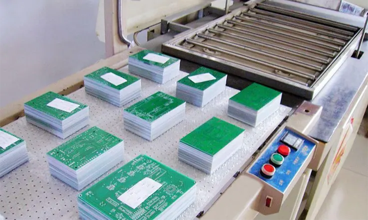
PCB Fabrication: Drilling, Plating, and Etching
The PCB fabrication process involves several detailed steps that convert raw materials into the conductive pathways that allow the Universal PCB to function. This stage includes drilling, plating, and etching, all of which are necessary to build a sturdy and functional Universal PCB. Let’s take a look at what each process entails.
Drilling-
In the drilling phase, holes are created in the PCB to make space for through-hole components, vias, and mounting pins. This step is carried out using high-precision CNC machines to ensure exact hole placement and size. The size of the holes varies depending on the type of component and the board’s design requirements.
| Hole Type | Typical Application | Hole Size Range |
| Through-Hole | Component leads and vias | 0.2mm – 1.5mm |
| Blind Via | Internal connections | 0.2mm – 1.0mm |
| Buried Via | Hidden layer connections | 0.2mm – 0.8mm |
Tip: The diameter of the holes influences the overall design, so it is must to consider component leads and the number of layers when selecting hole sizes.
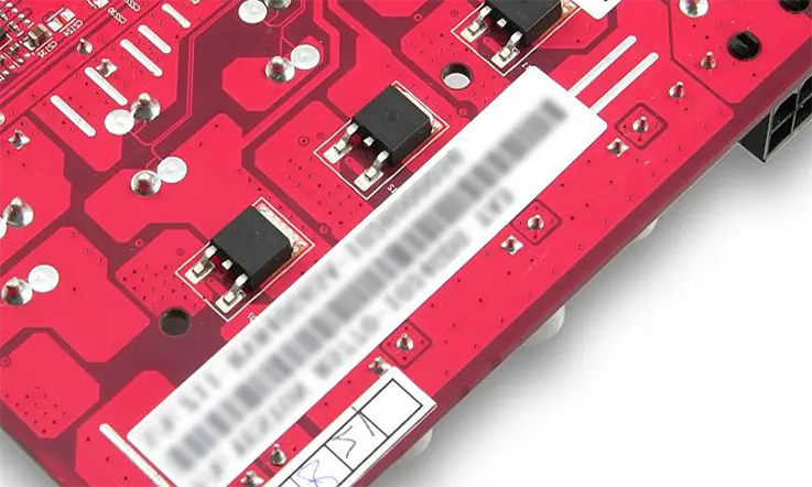
Plating-
Once the holes are drilled, plating is used to coat the inner walls of these holes with copper, ensuring that the electrical pathways connect the various layers of the PCB. The plating process is what allows the board to support multi-layer designs and ensures electrical continuity between different sections of the PCB.
Etching-
After plating, the excess copper is removed through the etching process. A chemical bath or laser technology is used to remove copper from unwanted areas, leaving behind the desired electrical traces. This process defines the circuit paths that connect different components on the Universal PCB.
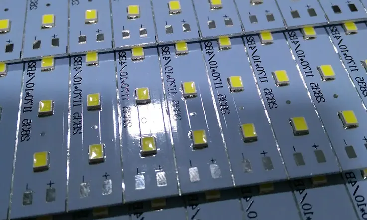
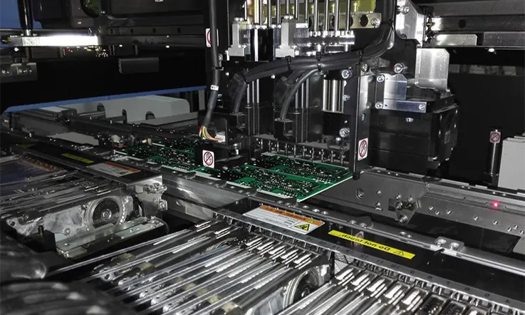
Assembly Techniques: Wave Soldering and Hand Soldering
Once the PCB is fabricated, it’s time for assembly. There are different techniques used to attach the components to the Universal PCB, with wave soldering and hand soldering being two of the most common. Let’s examine both processes and when each is appropriate.
Wave Soldering-
Wave soldering is a well-established method used to solder through-hole components onto a PCB. In this process, the board moves over a wave of molten solder, which connects the component leads to the PCB pads. It’s a very efficient method for bulk soldering, as it can solder multiple components at once. This technique is especially useful for larger production runs of Universal PCBs.
Hand Soldering-
While wave soldering works well for high-volume production, hand soldering is often employed for smaller production runs or for specialized components. With hand soldering, an operator uses a soldering iron to manually attach component leads to the pads on the PCB. This method provides more precision, especially for small components or components that are difficult to reach with wave soldering.
Hand soldering also offers flexibility in situations where modifications or repairs need to be made to the board. It’s a slower process compared to wave soldering but remains an essential technique for certain scenarios.
Inspection and Testing: AOI, Functional Test, ICT
Once assembly is complete, it is necessary to verify the Universal PCB’s performance and quality. Several methods are used for inspection and testing, including Automated Optical Inspection (AOI), Functional Testing, and In-Circuit Testing (ICT). These processes help identify any issues that may have occurred during fabrication or assembly.
Automated Optical Inspection (AOI)-
AOI is a visual inspection process where high-resolution cameras and computer software scan the PCB for defects such as missing or misplaced components, soldering issues, or incorrect component orientations. This is particularly useful in high-volume production runs of Universal PCBs, as it enables quick, automated detection of problems before the board is shipped.
The AOI system compares the real-time image of the Universal PCB to a reference image based on the design specifications. This process helps ensure that any defects are identified early and resolved quickly.
Functional Testing-
Functional testing checks whether the Universal PCB performs its intended functions. This test goes beyond simply looking for physical defects and examines how the board operates within a larger system. In consumer electronics, for example, functional testing might involve powering up the board to simulate its use, checking whether all signals are correctly processed and if the board performs according to the specifications.
In-Circuit Testing (ICT)-
ICT is used to check the electrical properties of the Universal PCB after assembly. It involves testing each individual circuit and component on the board to confirm they are connected properly and functioning as they should. This type of testing helps detect issues like open circuits, short circuits, and improper connections. ICT is often used for high-density designs where manual inspection would be difficult.
Universal PCB Materials and Laminates: Choosing the Right Substrate
When designing a Universal PCB, selecting the right base material shapes everything from thermal performance to signal behavior and mechanical handling. Engineers working with consumer electronics, wearable devices, and embedded systems often rely on substrate characteristics to match project requirements and production tolerances. This section breaks down three widely used substrate materials and examines how they influence electrical, thermal, and structural attributes—while also addressing compliance aspects tied to flame resistance and environmental standards.
Comparing FR-4, CEM-1, and Ceramic Substrates
Universal PCBs can be built using a range of substrates, each suited for specific assembly techniques and performance conditions:
●FR-4: A fiberglass-reinforced epoxy laminate known for consistent dielectric behavior. It’s well-suited for multilayer designs and supports both through-hole and surface-mount components, making it suitable for wearable electronics, communication modules, and automotive prototypes.
●CEM-1: A composite made from woven glass and paper-based laminate, commonly applied in single-sided PCB production. Its moderate strength and lower cost make it appealing for lighting devices and household electronics.
●Ceramic Substrates: Typically built with aluminum oxide or aluminum nitride, these offer strong thermal conductivity and electrical insulation. They’re often used in power electronics, LED lighting, and high-frequency RF systems, where heat dissipation and signal stability are essential. However, ceramic boards require extra care during handling and assembly to avoid material fracture.
Each option serves specific use cases within the Universal PCB manufacturing space, and selecting between them should involve a careful review of electrical specs, heat constraints, and mechanical limits.
How Material Impacts Thermal, Electrical, and Mechanical Properties?
Base materials affect how a Universal PCB handles temperature changes, signal transmission, and physical stress. Here are the main property categories to consider:
●Thermal Behavior: FR-4 typically offers a thermal conductivity around 0.3 W/m·K, which is manageable for low-power designs. Ceramic substrates—especially aluminum nitride—can exceed 20 W/m·K, offering stronger thermal performance in high-power applications.
●Electrical Behavior: FR-4 maintains stable dielectric constants, helping with impedance control in multilayer circuits. CEM-1 may fall short under high-speed or RF signal conditions due to higher dielectric losses.
●Mechanical Strength: While ceramic boards offer rigidity, they’re more prone to cracking under vibration or mechanical shock. FR-4 is better suited for flex and bend tolerance during manufacturing and daily operation.
Engineers should balance these properties based on the target device’s thermal footprint, signal frequency, and expected stress profile across its lifecycle.
Flame Resistance and RoHS Compliance Considerations
Universal PCBs must meet safety and regulatory benchmarks, especially when used in healthcare equipment, consumer products, or systems intended for international markets. Here’s what to keep in mind:
●Flame Rating: FR-4 materials usually comply with UL94V-0 standards, offering self-extinguishing behavior under controlled lab conditions. Ceramics are naturally flame-resistant due to their inorganic composition, but their use must align with appropriate soldering and sealing techniques.
●Environmental Compliance: Universal PCB substrates should meet RoHS (Restriction of Hazardous Substances) directives, limiting exposure to substances like lead, cadmium, and mercury. Procurement processes should include verification of compliance certificates from laminate and solder paste suppliers.
●Packaging and Process Compatibility: Flame-resistant resin layers and halogen-free bonding materials can help meet environmental safety expectations. Ensuring that all stack-up materials conform to these thresholds helps avoid costly redesigns or export restrictions down the line.
To minimize delays or compliance concerns, consider reviewing flame resistance and RoHS compatibility during the material selection phase—not just at final inspection.
Advanced Stack-up and Layer Design in Universal PCBs
Layer configuration and stack-up planning in Universal PCBs directly influence electrical performance, manufacturability, and signal behavior. Applications such as wearable electronics, industrial control systems, and compact instrumentation often require designs that manage high-frequency signals, power integrity, and dense routing. A systematic approach to stack-up structure ensures consistent impedance control, controlled return paths, and practical routing space allocation. The following sections outline foundational techniques in signal handling, layer distribution, and grounding for Universal PCB projects.
Signal Integrity in High-Speed Applications
Maintaining signal quality in Universal PCBs requires attention to high-frequency signal propagation, impedance matching, and noise suppression.
Core practices include:
●Controlled Impedance Design: Define precise trace widths, spacing, and dielectric thickness based on calculated impedance targets, especially for differential pairs and RF paths.
●Dielectric Material Management: Use low-loss laminates such as high-Tg FR-4 or polyimide for better propagation characteristics and reduced signal attenuation.
●Via Stub Reduction: Shortening via stubs through back-drilling or employing blind vias helps reduce reflection and resonance in high-speed paths.
●Consistent Return Paths: Ensure uninterrupted reference planes below signal traces to reduce loop inductance and improve signal return quality.
High-speed signal quality is influenced not just by trace width, but by the electromagnetic environment created through layer design and dielectric consistency.
Layer Count and Via Type Optimization
Optimizing the number of layers and the types of vias used improves routing efficiency and electrical performance, especially in compact or high-density boards.
Recommended strategies:
●4- and 6-Layer Configurations: Provide effective separation of signal, power, and ground layers for controlled impedance and reduced EMI.
●Via Selection by Function: Use through-hole vias for simple interconnects, blind/buried vias for HDI layouts, and microvias for fine-pitch BGA components.
●Copper Distribution Balancing: Maintain symmetrical copper coverage across layers to prevent warping during lamination and soldering.
When planning for manufacturability, layer stack-ups must also account for press-out thicknesses and drill aspect ratios in the fabrication process.
Ground Plane and Power Distribution Strategies
Ground and power layout affects voltage consistency, noise margins, and electromagnetic compatibility. Proper implementation helps stabilize circuit operation and simplifies compliance during system testing.
Implementation guidelines:
●Dedicated Power and Ground Planes: Use full copper layers rather than isolated pours to reduce impedance and support decoupling performance.
●Capacitor Placement: Position decoupling capacitors close to power pins and distribute them evenly across the board to minimize local noise.
●Analog-Digital Isolation: Segment analog and digital grounds and rejoin at a single reference point to reduce signal coupling across domains.
Clean separation of return paths and proper decoupling can prevent voltage fluctuations and support steady operation across all active components.
Universal PCBs for Low-Volume and High-Mix Manufacturing
In sectors such as industrial instrumentation, medical diagnostics, and specialized consumer devices, demand for diverse PCB variants in limited production runs continues to grow. Universal PCBs support this shift by offering layout compatibility across multiple use cases without redesigning core infrastructure. These configurations simplify board revisions and accelerate delivery for pilot builds and limited production schedules.
The following sections outline how turnkey assembly support, flexible BOM handling, and rapid prototyping workflows enable more responsive product iterations in low-volume, high-mix settings.
Niche OEM Production with Turnkey PCB Assembly
Turnkey assembly streamlines operations by integrating fabrication, component sourcing, and final assembly into a single service pipeline. For niche OEMs or custom device builders, this approach minimizes lead times and limits logistical overhead.
Implementation practices include:
●Shared Universal PCB Platforms: Using a single base layout across variants reduces engineering cost per product line.
●SMT and THT Mixed Processes: Supporting both mounting methods accommodates legacy components and specialty parts without custom redesign.
●Single-Vendor Coordination: Turnkey models centralize responsibility for quality, documentation, and delivery schedules.
OEMs pursuing small batch manufacturing often favor providers with integrated ERP tracking, reflow and wave soldering capabilities, and test fixture development options. These service combinations maintain consistency across revisions while simplifying quality control.
Rapid Prototyping for Startups and Hardware Incubators
Startups and engineering incubators frequently rely on rapid iteration to meet investor milestones or refine proof-of-concept units. Universal PCBs support quick adaptation through reusable layouts and DFM-verified stack-ups.
Applied approaches include:
●Modular Footprint Planning: Reserve headers or configurable zones for testing pinouts, sensor swaps, or microcontroller upgrades.
●Quick-Turn Fabrication: Partner with fabs offering 2–5 day lead times with material preset options (e.g., FR-4, TG170) for reliable electrical behavior.
●Test Point Integration: Design for easy oscilloscope or multimeter access during firmware debugging.
Hardware teams often favor universal footprints that support footprint-compatible components such as ATmega328P vs. STM32F103 or ESP32-WROOM vs. ESP32-C3 to allow flexibility at the firmware level without routing changes.
BOM Optimization and Component Sourcing for Flexibility
Component availability directly affects production planning in low-volume environments. Universal PCBs that accept a broader range of alternate parts avoid delays caused by single-source shortages.
Execution strategies include:
●Dual Footprint Pads: Design pads compatible with both SOT-23 and SC-70 for voltage regulators or analog switches.
●Tolerance-Based Passive Selection: Use wide-tolerance resistors (e.g., 1% vs. 5%) where function permits, increasing sourcing options.
●Pre-Approved Substitutes in ERP: Maintain alternate part numbers in the bill of materials to enable on-the-fly procurement.
Suppliers such as Mouser, Digi-Key, and LCSC now support real-time API connections for BOM checking, which helps avoid manual sourcing delays and flags lifecycle concerns early in the project.
Thermal Management and Reliability Engineering on Universal PCBs
Universal PCBs used in power-dense or long-cycle applications must be designed to handle thermal stress and maintain mechanical and electrical stability over time. As operating currents increase or duty cycles grow longer, thermal buildup becomes a performance limiter. By applying deliberate design measures—such as copper pouring, proper thermal relief, and process-specific coatings— many manufacturers can mitigate risks tied to overheating and aging-related degradation. The following sections break down thermal pathways, heavy-current design approaches, and material-based reinforcement techniques for long-term durability.
Heat Dissipation Using Copper Pours and Thermal Pads
To avoid excessive thermal gradients across the board, passive heat control elements are frequently integrated directly into the layout. These techniques support efficient temperature distribution and help prevent localized stress.
●Copper pours — Broad copper areas on internal or outer layers provide heat-spreading zones, reducing hot spots under active components. Ground pours often double as thermal mass in power systems.
●Thermal vias — Vias placed beneath heat sources transfer thermal energy to internal copper planes or the opposite PCB surface. Filling or plating these vias with conductive material enhances the conduction path.
●Thermal relief patterns — For components with high dissipation, thermal pads under QFNs or regulators must be isolated with carefully spaced copper fingers to avoid excessive reflow dwell time.
●Component spacing — Increasing the clearance between high-power parts helps reduce heat interference, particularly in enclosures lacking airflow.
Example Table: Heat Dissipation Methods
| Thermal Control Technique | Function | Typical Application | Design Consideration |
| Copper Pours | Heat spreading and electrical grounding | Power delivery zones, RF shielding | Connect to ground plane to dissipate heat evenly |
| Thermal Vias | Vertical heat transfer to inner layers | Underneath QFNs, power ICs | Fill or plate with conductive paste for efficiency |
| Thermal Relief Patterns | Prevents overheating during soldering | QFN pads, regulator footprints | Maintain thermal isolation around component pad |
| Component Spacing | Reduces heat accumulation | Multi-power IC layouts | Use 2–3 mm spacing to allow thermal breathing |
High-Current Applications with Universal Boards
Universal PCBs used in motor drivers, battery chargers, and lighting systems often carry elevated current levels, which require special design measures beyond standard trace rules.
●Trace width and thickness — Following IPC-2221 current capacity guidelines, traces are widened and copper thickness may be raised to 2 oz or more on power planes.
●Heavy copper integration — When continuous operation above 10 amps is expected, heavy copper routing or bus bar additions may be considered.
●Board stack-up — Symmetrical layering helps offset warpage from uneven heating, especially where power layers are placed near surface routing.
●Fuse integration and test pads — Inline fuses or jumper pads aid protection and testing during production and post-assembly validation.
Implementing these steps early in layout minimizes the need for rework or thermal shielding in final assembly.
Example Table: High-Current Design Parameters
| Parameter | Standard Value (1 oz Cu) | Enhanced Value (2 oz Cu) | Application Example |
| Max Trace Current (1 mm width) | ~2.3 A (internal layer) | ~3.5 A (external layer) | Battery management PCB |
| Heavy Copper Routing | Not used | ≥3 oz copper | Motor controller board |
| Recommended Trace Width for 10A | 2.5 mm (min) | 1.3 mm (with 3 oz copper) | Automotive lighting PCB |
| Fuse Rating Range | 0.5 A – 30 A | Configurable via design | Integrated inline test pads |
Ensuring Long-Term Performance with Coatings and Pre-bake
Moisture absorption and oxidation can degrade electrical integrity and solder bond quality over time. Applying material protections during pre-assembly and post-assembly processing helps maintain dimensional and electrical stability.
●Pre-baking prior to reflow — Boards stored in uncontrolled environments may absorb moisture, which can cause delamination or blistering during solder reflow. Pre-bake steps remove absorbed moisture before assembly.
●Conformal coatings — Acrylic, polyurethane, or silicone coatings shield circuits from chemical vapors, salt spray, and surface tracking during field deployment.
●Edge masking and selective protection — Areas not covered by coating—such as connectors or thermal pads—should be masked during application to preserve conductivity and bonding.
●Surface finish stability — ENIG and immersion silver finishes resist oxidation better than HASL for extended shelf-life and solderability.
Applying these practices not only supports environmental endurance but also meets manufacturing requirements in consumer, industrial, and automotive contexts.
Example Table: Protective Measures for Long-Term Durability
| Protective Measure | Purpose | Typical Material or Process | Deployment Environment |
| Pre-Baking | Moisture removal before reflow | 125°C for 4–6 hours | Humid storage or aged PCBs |
| Conformal Coating | Prevents corrosion, dust, salt spray | Acrylic, polyurethane, silicone | Marine, industrial, outdoor |
| Selective Masking | Preserves pad contact points | Peelable mask or tape | Connectors, test pads |
| Surface Finish | Maintains solderability | ENIG, Immersion Silver | Long storage, harsh climate |
Testing, Inspection, and Quality Control in Universal PCB Manufacturing
Maintaining consistency in Universal PCB production requires a structured testing and inspection framework that addresses every phase—from bare board verification to post-assembly diagnostics. For small-batch and high-mix scenarios, we must to prioritize flexible inspection methods and adaptable test routines. This section provides technical coverage of standard practices used to verify structural, electrical, and functional conformance without resorting to rigid inspection templates.
Visual and Automated Optical Inspection
This phase focuses on identifying surface anomalies before moving forward with functional testing. Both manual and automated methods are used to examine solder joints, component alignment, and mounting precision.
●Manual visual inspection: Operators examine PCBs under magnification to detect solder bridging, cold joints, missing parts, and polarity mismatches.
●2D automated optical inspection (AOI): Scans PCB surfaces for placement deviations and solder coverage inconsistencies after initial SMT processes.
●3D AOI systems: Capture solder volume and height data post-reflow to evaluate joint structure and shape consistency.
●Reference-based defect detection: AOI software compares boards against golden images to flag deviations from predefined tolerances.
●Advanced illumination techniques: Variable-angle lighting enhances detection of lifted leads and tombstoned components.
Testing Methods for Manual and Machine Assembly
Thorough electrical testing confirms circuit continuity, signal behavior, and functional reliability across production batches. Selection of test method depends on complexity, layout density, and production scale.
●Flying probe testing: Suitable for small lots and prototypes; enables pin-to-net verification without custom fixtures.
●In-circuit testing (ICT): Applies fixed probes to confirm correct values, polarity, and component placement on mass-produced boards.
●Boundary scan techniques: Used when physical access to test nodes is restricted; applicable to high-density ICs and BGA packages.
●Functional testing: Involves simulation of end-use scenarios with controlled power and signal inputs.
●Manual probing: Performed by technicians using multimeters or oscilloscopes, primarily during engineering validation or troubleshooting.
Defect Prevention in Small Batch Production
In small-quantity manufacturing, the relative impact of a defect is higher, requiring early-stage controls and traceability practices.
●First article inspection (FAI): A full inspection of the first assembled unit, with documentation for traceable compliance before further production.
●Solder paste inspection (SPI): Evaluates stencil printing accuracy to reduce solder bridging and open connections.
●Design-for-test (DFT) integration: Encourages inclusion of test points, consistent pad access, and test fixture compatibility at the design level.
●Standardized operator guidance: Clear assembly instructions and visual references reduce manual errors on small production lines.
●Closed-loop feedback: Quality data is recorded and reviewed to inform layout improvements and process tuning in future revisions.
FAQ: Universal PCB
Q1: What challenges exist in Universal PCB design for low-volume production?
A1: Challenges include higher setup costs, limited component availability, and the need for rapid prototyping while balancing cost-efficiency with customization.
Q2: How does temperature affect the lifespan of Universal PCBs?
A2: Temperature fluctuations can lead to delamination or brittleness in PCBs. Proper thermal management techniques, like copper pours, help maintain stability.
Q3: How does multi-layer PCB technology apply to Universal PCB design?
A5: Multi-layer PCBs allow for compact designs and complex circuits, improving performance without increasing size, but require optimized layer stacking and signal integrity.
Q4: How does component packaging affect Universal PCB design?
A8: The choice of packaging impacts pad sizes, via types, and spacing, influencing the overall design and performance of the PCB.