
In the process of “designing for manufacturability,” also known as “DFM,” one of the most important steps is “designing for testability” in a printed circuit board design (DFT). This fundamental idea can be summed up as the process of designing a product that is consistent at the lowest possible cost to manufacture it while keeping an acceptable fault rate.
When designing a PCB, it is important to keep testability in mind throughout the entire process. This requires describing the creation process so that test point requirements can be understood and flaws can be located quickly. In order to design for maximum profitability, DFT is an absolute necessity, both for the prevention of manufacturing errors and the resolution of component failures. Within the scope of this study, we shall investigate DFT of printed circuit boards in great detail.
Design for Testability Tips to Think About When Making Your PCB
● When a contract manufacturer is looking over a design for testing, the very first thing they will do is examine the customer test specification that has been provided. With the use of this data, it will be possible to devise a testing procedure that will satisfy the standards. Even though the CM test engineers have the ability to develop their own specification if it becomes required, it is best practice for you to provide as much information as you can to your CM in order to ensure that the board is thoroughly tested in accordance with the requirements of the customer.
● As part of their testing evaluation, the CM will also examine the layout and mark the schematic with test and connection points. Another useful design practice is to provide particular test points in the schematic to assist the CM with this preparation.The design evaluation, in conjunction with the test methodology, will assist in determining the kind of fixture that is required, as well as whether or not any adjustments to the design are indicated to increase the effective fault coverage of the test procedures. The entirety of this material is subsequently included into a test instruction (TI) document, which is supported by descriptions, images, and expectations for the test technicians to utilize during the actual testing.
● One of the objectives of the review is to identify whether in-circuit testing (ICT) or flying probe will be performed. Each of these processes has benefits and drawbacks that must be weighed when making a final decision:
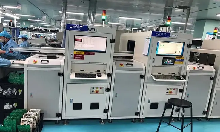
Because it is so simple to set up, flying probe testing is ideally suited for use in prototyping and in low-volume production runs. This is mostly owing to the fact that flying probe testing requires very little setup time. The ability to readily adapt the test programming of the flying probe is an additional benefit that is an added bonus in light of the consistent layout adjustments that are made to prototypes. When compared to ICT, flying probe testing is slower than other methods since an individual flying probe must be used to contact each test point on the board. The ICT fixtures and fixed programming are perfect for producing bigger quantities of established board designs during manufacturing runs of longer duration.
Parameters To Include in DFT
As its name implies, PCB DFT (Design for Testability) does require specific design tasks to be undertaken before it can be implemented during the PCB manufacturing phase of product development. This typically involves adding test points, headers, LEDs, test wires, other undocumented features to the board so that parameters of interest may be directly calculated or monitored, hence accelerating validation testing.
In order to make sure that your tests are accurate and efficient, here are some of the parameters that you might include in them:
LEDs:You can place LEDs wherever their use will be maximized. For instance, a DONE signal on a power supply sequencer to indicate that the device has been powered on. Or, debug LEDs on FPGAs, microcontrollers, etc., which can be utilized to reveal code errors. They can be removed from the bill of materials (BOM) at a later date, but they’re great when you have a prototype that isn’t quite ready for prime time, so you can see what’s going on.
Test Traces:You might just layout some traces that imitate other sensitive traces so that you can play with them if there is space available to do so. Install test points or connections on them so that you can connect them to other devices, such as scopes, TDRs, signal generators, etc., and view what the prospective appearance of your other signals could be. Alternately, if you have any unused clock outputs, you might run one of them to a connection. This could come in handy for triggering or synchronization purposes while the device is being tested.
Test Points:You will have test points for the fixture if your design undergoes ICT (in-circuit testing). You will likely attempt to arrange these so that signal integrity problems are minimized. However, they can also be arranged to make your design easier to probe. Aligning them for a differential probe tip at the end of the signal trace that is of interest is one example. Or, by establishing ground and power test-points in key locations where I am anticipating conducting a significant amount of investigation.
Headers:You are able to add a multitude of headers, the most of which will not be included on the final bill of materials (BOM). Putting in headers for the main voltage rails so that there will be a simple spot to connect a cable or a DMM for checking the chamber, etc. In addition, wherever there is a JTAG port on programmable logic, a header that is compatible with the programmer should be attached. I2C busses are able to withstand a certain amount of SI sloppiness, which is why I added headers to them. For the sake of debugging or conducting experiments at a later time, unused I/O from a CPLD, FPGA, or microcontroller might be routed to a header.
Undocumented Features:If you have sufficient space and spare time, you could even be able to design and implement a full experimental circuit or additional function that you do not intend to ship. It might make it possible for you to try out a fresh concept. It’s possible that you did this at some point in the past in order to test out different minimum loadings for a power supply. Or it might give you greater access for debugging, like a USB port for your embedded device, which you could use if it does. However, doing so requires additional time and board space to be allocated.
What Are the Design for Testing Techniques?
The two most significant techniques of testing are as follows:
1. Bare Board Testing
Before putting the components together, bare board testing is done to verify the connectivity of the PCB. The three methods for conducting this type of testing are as follows:
● Continuity Testing: A check for continuity is performed on the circuit board to determine whether or not it has any open circuits.
● Isolation Testing: Through the isolation test, the resistance between two electrical connections is confirmed.
● Short Circuit Testing: Checking for the presence of any unintentional electrical connections that may have been created as a result of a manufacturing error or a design error is required here.
Bare-board tests are derived from a netlist, which in turn is derived from the data you provide for your design. The design files will contain a netlist if you send your design data to your CM in the ODB++ data format. If you continue to use Gerber files, the CAM department will create a netlist from the schematic and Gerber files that is subsequently used for bare board tests. Bare-board testing might shorten the time required to test your PCB by using flying probe or bed of nails tests.
2. Assembled Board Testing
After the board has been assembled, an ICT is done to help isolate shorts, open circuits, and damaged components. Instead of doing it by hand, a flying probe or bed of nails ICT will give automated testing and boost your test coverage.These tests will confirm that the connections in the schematic and netlist correspond to the actual connections in your PCBA. These automated ICT tests have a low upfront cost and may validate connectivity performance. The integrity of the circuit boards and proper component functionality are both guaranteed by this method.
Functional Testing of DFT
Functional testing is a related testing process in which the electrical functioning of the board is measured while the board is operating. Your CM will make extensive use of test points and test structures here in order to validate the integrity of interface connectors, as well as connection, timing, and the overall performance of the board.
In most cases, the needs for functional testing of your board may be ascertained during the design review process; however, there may be particular features of your board that call for further in-depth testing. By including annotations in your schematics, you can make sure that the performance criteria and tolerances you’ve specified are clear.
If your board needs to communicate with another system or if it has other specific requirements, your CM may be required to use a variety of test fixtures, perform some data collecting and processing in LabVIEW, or use an upper-assembly test environment that you provide.
The combination of ICT and functional testing increases yields, offers more accurate data for troubleshooting, and maintains the product’s reliability throughout its lifecycle. The most exhaustive test coverage will be provided by a JTAG test, an automated ICT test, X-ray laminography, and visual inspections.
JTAG Test
JTAG test techniques can be utilized to handle numerous demands in addition to simple structural testing requirements, despite the fact that they were initially intended to meet the requirements of testing printed circuit board assembly (PCBA) interconnects. The majority of JTAG and boundary-scan systems are made up of two primary components: a test program generator, which is responsible for the conception and creation of tests, and a test program executive, which is responsible for performing tests and reporting findings.
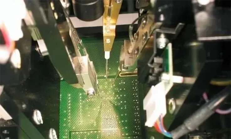
Flying Probe Test
The flying probe test is a type of non-invasive ICT (Inc-Circuit Test) that measures continuity, open and short circuits, and passive component values. This test was developed so that it could be used on prototypes and in small production runs. In order to use the flying probe test, the PCB designer and the contract manufacturer need to work together and complete the following stages:
Step 1: Determine the parameters to be measured. Values for passive devices such as resistors, continuity for devices such as diodes, and connectivity, including open and short circuits, are examples of parameters.
Step 2: In the areas of your PCB layout where probe access points (vias and through holes, for example) are not already present, you should add test points.
Step 3: Flying probe tester needs to be programmed to stop at the necessary test places on the PCB assembly.
Step 4: Run the test and gather test result data.
If you want complete coverage of your PCB, you can use the following principles to figure out where test points are needed and whether or not they are necessary:
● Use thru-hole pins as test points.
● Use surface mount pads as test points.
● Use standard and blind vias as test points.
● Add test points to otherwise inaccessible nets.
Setting up the flying probe test, as well as scripting and carrying it out, might take a significant amount of time, potentially even several days. On the other hand, even in the event that a redesign is required, there are typically only minor adjustments to be made to the testing protocol.
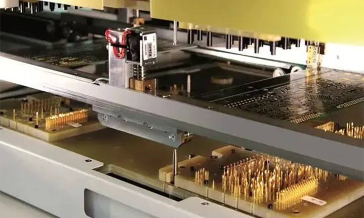
Bed of Nails Test
For both the bed of nails test and the flying probe test, the steps required of the PCB designer and contract manufacturer are comparable. Despite the fact that both tests require setup time before they can be performed, the bed of nails test requires the construction of a separate apparatus. This adds significant expense and time to the PCB manufacturing phase; in fact, the development setup time can extend to several weeks. However, the bed of nails test itself may be conducted rapidly and is suitable to production runs.
The bed of nails test can provide more specific information than the standard flying probe test. This consists both analog and digital data, as well as some integrated circuit functioning data. Nevertheless, certain soldered pads may be excluded from the bed of nails test due to physical constraints. Consequently, it is crucial to contact with your contract manufacturer early on to ensure that any such limits are accounted for in your PCB DFT.
ICT Test
Testing using ICT can uncover a variety of flaws in Printed Circuit Boards (PCBs), both in the manufacturing process and in the components themselves. ICT testing systems can be divided into two categories. In one configuration, the test is carried out by means of a test fixture that clamshells the printed circuit assembly (PCA) that is being evaluated and probes a number of different nets. The second type of test is known as a flying probe test, and it involves making electrical contact with particular nets of the PCA that is being evaluated using probes that are controlled by a computer system.
Some examples of PCB design testing look for shorts, openings, missing components, components placed with the incorrect polarization or even the incorrect value, among other things. In addition, ICT testers can power the PCA under test and exercise analog and digital circuits to ensure appropriate performance. This regimen of tests can be performed at a high volume throughput by ICT test point systems.
X-ray Inspection
X-ray inspection technology, also known as automated x-ray inspection technology, is a technique that can discover hidden features within a target object. This technology was developed by the General Electric Company. X-ray inspection is a process that is frequently used to uncover production faults across many different industries, including the medical and aerospace manufacturing industries. It is especially common in PCB inspection since x-rays are a good way to assess PCB quality and detect hidden problems without putting the board at risk of being damaged.
Manual Visual Inspection
Manual Visual Inspection (MVI) is a process that is used in the production of printed circuit boards (PCBs) in which an individual inspects a PCB and compares it to a “Golden Board” or against certain quality control criteria that are included in the quality control inspection check list. Before the printed circuit board (PCB) is incorporated into the finished product, it will first undergo a visual inspection, which will help detect any flaws that may exist.
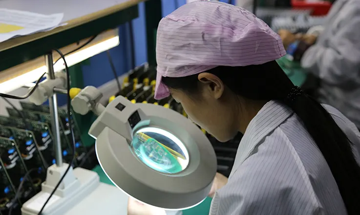
The most straightforward method of MVI is with the naked eye. However, this is unlikely to detect anything other than the most evident flaws, especially when analyzing smaller, denser PCBs. Therefore, the board is frequently examined under a microscope, which provides a more precise and detailed image of each component that makes up a functional PCB.
Conclusion
Suggestion of Jarnistech: Working With Your CM To Get the Best PCB Test Results
By giving your CM with a test specification, noting test and probe points in the schematic, and adhering to the minimum spacing criteria for test points in the layout, you will be well on your way to creating a completely testable PCB. However, there is something more you can do that would be useful, and that is to consult with your CM early on regarding your design. This manner, you can get answers to your queries and learn what is required to test your board effectively.
At JarnisTech, we have design, layout, and test engineers who have years of experience and are eager to collaborate with you on the design of your product. We are here to assist you with any queries or concerns regarding the design of your board as it relates to setting it up to be completely tested.


