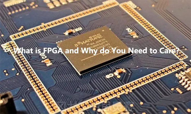
In recent years, the field of electronics has experienced significant advancements, particularly in the very large scale integration (VLSI) industry. Starting with the invention of the transistor and progressing to the development of the integrated circuit and application-specific integrated circuit, technology has advanced at an impressive pace.
Furthermore, the advent of programmable logic devices (PLDs) served as a crucial stepping stone towards the widespread adoption of fabless semiconductor technology. Although PLDs were initially developed in the early 1970s, it was not until Xilinx introduced field programmable gate arrays (FPGAs) in the late 1980s that they became widely used in the ASIC realm.
Since then, PLDs, including FPGAs, have undergone significant improvements in terms of functionality and performance. As such, it is worth delving into the specifics of FPGAs and the advantages they offer.
What Is FPGA ?
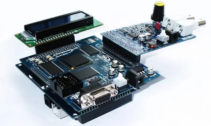
The Field Programmable Gate Array (FPGA) is a versatile type of integrated circuit that can be adapted to suit the unique needs of a specific application by utilizing user-programmable interconnects within its hardware blocks. An FPGA can facilitate the implementation of new functionalities throughout its lifespan due to its ability to reprogram its interconnects.
The design of FPGAs owes its origins to earlier devices like programmable read-only memories (PROMs) and programmable logic devices (PLDs). Though both PROMs and PLDs could be programmed either at the factory or in the field, their configurations were permanent and unalterable since they relied on fuse technology. However, FPGAs store their configuration information in reprogrammable mediums like static RAM (SRAM) or flash memory, offering greater flexibility.
Industry giants such as Intel, Lattice Semiconductor, Microchip Technology, and Microsemi are among the top manufacturers of FPGAs.
FPGA Architecture and Components
FPGA (Field Programmable Gate Array) consists of several architectural and component elements that enable users to program the circuit according to the required functionality. Here are some of the main architectural elements of an FPGA:
● Configurable Logic Blocks (CLBs): These are the basic building blocks of FPGAs, consisting of lookup tables (LUTs) for combinational logic, and flip-flops for sequential logic. In addition, some modern FPGAs have built-in math operations units, which come in handy for DSP applications.
● Programmable Interconnect: The interconnection gives the CLBs the tunnels through which data passes and by which signals from input and output pins are connected to the LUTs and flip-flops. In modern FPGAs, the interconnect uses a hierarchy of different types of routing wires, each with different speeds, directions, and lengths.
● Input/Output Blocks (IOBs): IOBs allow external signals to communicate with the internal CLBs and perform parallel or serial interfacing with other digital circuits/systems. The IOBs can handle a combination of single-ended, voltage-regulated, or differential signals and external clock signals.
● Embedded Memory Blocks: Some FPGAs have embedded memory blocks such as block RAM or FIFO buffers, available for designers to use either as a standalone memory or as an interconnection medium between modules.
● Digital Signaling Processing (DSP) Blocks: DSP blocks in the FPGA consist of multiple arithmetic circuits for performing complex math operations such as multiplication, division, and addition efficiently.
● Clock Management: FPGAs can offer various clock methods to ensure reliable and jitter-free clocking of internal modules or to connect to external synchronization requirements.
● Configuration Memory: The FPGA configuration information is stored in non-volatile memory such as Flash, ferroelectric, electrically erasable programmable read-only (EEPROM), or volatile Static RAM (SRAM), which will configure the FPGA at each start-up.
The interconnection between all these elements is programmable after manufacturing, allowing FPGA devices to provide a unique flexibility of configuration according to the intended application domain.
Advantages and Disadvantages of FPGA
Advantages of FPGA
● Flexibility: FPGA’s hardware configurability offers flexible and adaptable system designs which can be reprogrammed and reconfigured as needed.
● High Performance: FPGA’s parallel architecture can offer high performance, making it an excellent choice for applications requiring real-time processing and high-speed data processing.
● Lower Power Consumption: FPGA designs can offer lower power consumption compared to a software solution running on a CPU. This is because only the resources required to perform the task are used, and idle circuits are not powered up.
● Lower Cost: FPGA designs can offer a lower per-unit cost compared to ASICs designed for low volume applications, because the FPGA can be used for many different applications.
● Shorter Time to Market: FPGA provides shorter design cycles and reduces the time to market compared to a custom ASIC solution.
Disadvantages of FPGA
● Complexity: FPGA development can be challenging due to its complexity. Successful implementation requires extensive knowledge of digital logic design, hardware description languages, and FPGA technology.
● Higher Cost: High configuration costs of FPGAs as the initial investment is needed to buy the hardware and software design tools required for development.
● Limited Resources: FPGAs have limited resources compared to dedicated ASICs. This can result in limitations on the size and complexity of the designs that can be implemented.
● Limited Support: FPGAs requiring specialized knowledge of programming languages, and application programming interfaces (APIs) and hardware environments, that can limit technical support options.
Bitstream Security Concerns: Since bitstream is configurable data that controls the FPGA hardware functionality, it can be vulnerable to a malicious attack that alters the FPGA function.
FPGA Applications
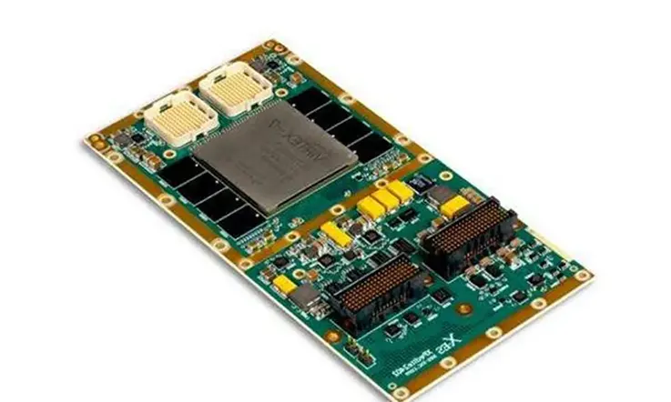
The versatility of Field Programmable Gate Arrays (FPGAs) makes them a suitable option for numerous industries. As an industry leader, AMD provides comprehensive solutions for a diverse range of markets and applications. AMD’s offerings encompass FPGA hardware, advanced software, and configurable IP cores that are ready to be utilized.
AMD’s FPGA solutions are applicable to several markets and use cases, including:
●Wireless Communications: solutions for RF, base band, connectivity, transport, and networking for wireless devices, addressing standards such as WCDMA, HSDPA, and WiMAX amongst others.
●Wired Communications: Complete solutions for the Reprogrammable Networking Linecard Packet Processor, Framer/MAC, serial backplanes, and other components of the network.
●Aerospace & Defense: FPGAs that are resistant to radiation combined with the intellectual property necessary for image processing, waveform synthesis, and partial reconfiguration of SDRs.
●ASIC Prototyping: The use of field-programmable gate arrays (FPGAs) for ASIC prototyping enables rapid and precise modeling of SoC systems as well as verification of embedded software.
●Video & Image Processing: For a variety of video and image applications, AMD FPGAs and tailored design platforms allow better levels of flexibility, quicker time-to-market, and reduced total non-recurring engineering expenditures (NRE).
● Automotive: Providing automotive silicon and intellectual property solutions for gateway and driving assistance systems, as well as comfort, convenience, and in-vehicle infotainment systems.
● Security: Access control, surveillance, and other safety and security systems are just some of the areas in which AMD has developed solutions to satisfy the ever-changing requirements.
● Broadcast & Pro AV:With Broadcast Focused Design Platforms and solutions for high-end professional broadcast systems, you can adapt to changing requirements more quickly and lengthen the product’s life cycle.
● Medical:The Virtex FPGA family and the SpartanTM FPGA family can both be used to meet a variety of processing, display, and input/output interface requirements for applications such as diagnosis, monitoring, and therapy.
● Consumer Electronics:Converged handsets, digital flat panel displays, information appliances, home networking, and household set top boxes are all examples of next-generation consumer applications that can take advantage of cost-effective solutions.
● Industrial: Applications ranging from industrial imaging and surveillance to industrial automation and medical imaging equipment can all benefit from the increased flexibility, accelerated time-to-market, and decreased overall non-recurring engineering costs (NRE) made possible by AMD FPGAs and ISM-specific targeted design platforms.
● Data Center: Developed specifically for servers, networking, and storage applications that require high bandwidth and low latency in order to deliver a higher level of value to cloud deployments.
● HighPerformance Computing and Data Storage: Storage area networks (SAN), network-attached storage (NAS), servers, and storage appliances can all benefit from these solutions.
Programming Process an FPGA Design
Programming an FPGA involves describing the desired hardware functionality in a hardware description language (HDL), compiling the HDL code into a configuration bitstream, and then loading the bitstream into the FPGA. The general steps in programming an FPGA are:
● Design Entry: Write the hardware functionality in a HDL such as VHDL or Verilog, which describe the FPGA’s hardware behavior.
● Synthesis: The HDL code is translated into an optimized netlist, where the synthesis tool configures the FPGA with the desired functionality. This step creates a structural representation of the logic.
● Mapping: Mapping the synthesized netlist onto the FPGA architecture specified in the design.
● Placement: Placement of synthesized logic blocks on the FPGA floorplan that maximizes performance and timing.
● Routing: Creation and optimization of the interconnects, to connect the placed blocks together and to the input/output pins.
● Timing Analysis: Timing Verification and analysis to ensure the design timing requirements are correct.
● Bitstream Generation: Generation of a binary data file containing instructions for configuring the FPGA, known as “bitstream.”
● Configuration: Download the bitstream onto an FPGA device to configure the FPGA according to the specified design.
● Verification: Verify that the FPGA implementation matches the expected behavior.
Hardware description languages, such as VHDL and Verilog, offer a highly structured way of describing the behavior of digital systems and are used to create complex systems spanning a range of industries. FPGAs can also be programmed using high-level programming languages, such as C and C++, with the help of hardware design libraries such as High-Level Synthesis (HLS).
How FPGAs Work ?
FPGAs or Field Programmable Gate Arrays are integrated circuits that can be programmed or configured to perform specific tasks after manufacturing. Here is a high-level description of how FPGAs work:
● FPGA design: The first step is to create a design using a hardware description language (HDL) such as Verilog or VHDL. The design is usually created using a computer-aided design (CAD) tool.
● Synthesis: Next, the design is synthesized to produce a netlist, which is a high-level representation of the circuit.
● Place and Route: The place and route process takes the netlist and maps it onto the physical resources of the FPGA, including logic cells, routing switches, and input/output pins.
● Configuration: Once the netlist has been placed and routed, the FPGA must be configured with the appropriate settings using configuration memory such as flash memory or SRAM. This step sets the electrical path, logical connection and creates the interconnects between the devices.
● Operation: After configuration, the FPGA performs the programmed function and can be updated with new functions by reprogramming the configuration memory.
FPGAs can be reprogrammed repeatedly and can execute parallel operations as well as displaying lower power consumption in comparison to alternatives.
Why You Use a Field Programmable Gate Array ?
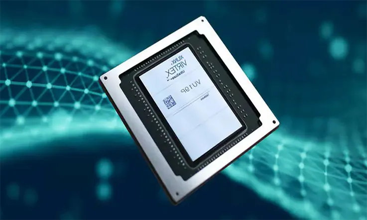
With FPGAs, you can tune your chip such that it can handle a high workload. So, when working with these chips, you may acquire the best possible outcomes. In addition to this, FPGA enables you to make later modifications at the chip level to produce the outputs that you want. Because of this level of adaptability, you are able to make significant modifications. For instance, you can adjust the power and memory use of your machine by making use of FPGA in order to save up on resource utilization. That could end up being a savior for your device in the end.
When it comes to the prototype of ASICs (Application-Specific Integrated Circuits) or Processors, FPGAs can prove to be quite helpful. This is due to the fact that you are able to re-program an FPGA until you obtain a final, bug-free Processor or ASIC that you are able to mass produce.
Comparison of FPGAs with Other Types of Programmable Logic Devices
FPGAs are one type of programmable logic device, and there are several other types available as well. Here is a comparison of FPGAs with other types of programmable logic devices:
● CPLDs (Complex Programmable Logic Devices): CPLDs are smaller and slower than FPGAs and generally used for simpler designs. They usually have a fixed architecture with a limited number of programmable elements.
● PALs (Programmable Array Logic): PALs are an early type of programmable logic device, and they have a fixed number of inputs and outputs. The logical functions are implemented using a programmable AND array followed by a fixed OR array.
● GALs (Generic Array Logic): GALs are similar to PALs, but they have additional programmable features such as flip-flops and control circuits, thus being more flexible than PALs.
● ASICs (Application-Specific Integrated Circuits): ASICs are custom-designed integrated circuits that are optimized for a specific application. They typically have higher performance and lower power consumption than FPGAs, but are more expensive and have longer design time.
Compared to CPLDs, PALs, and GALs, FPGAs are larger, faster, and more flexible. They offer a large number of programmable logic elements, optimized routing, and other features that allow designs to be implemented in a more optimized way. When compared with ASICs, FPGAs are more flexible at design time, provided design modifications are quicker and can be tested easily.
ASIC Vs. FPGA
Choosing between ASICs and FPGAs requires a thorough evaluation of each technology’s unique benefits. Numerous comparisons between the two types of technologies are available online. Historically, FPGAs were more suitable for designs with lower levels of complexity, speed, and overall volumes. However, modern FPGAs are capable of achieving performances of up to 500 MHz and beyond while boasting significant improvements in logic density, embedded processors, clocking, high-speed serial, and DSP blocks at increasingly affordable prices. As a result, FPGAs have become an attractive option for a broad range of designs.
Compared to microprocessors like ASICs, FPGA designs offer three significant advantages, particularly for prototypes or limited production runs. These advantages include:
● Performance of Flexibility: FPGAs are not often utilized in heavily parallelized processes due to the inability to match the performance of CPUs. Applications such as large image processing and digital signal processing require numerous cores and out-of-order instructions that current microprocessors execute better.
Furthermore, FPGA designs can incorporate several hard or soft microprocessors working together in a single chip. This integration eliminates the need to physically connect two separate devices, thus reducing the required space for the design.
FPGA design cycles require less manual intervention and are easier to manage due to their simpler nature. Routing, positioning, and timing are often handled automatically by the software to ensure compliance with specified criteria.
● Reusability: The versatility of FPGAs as reprogrammable and reusable devices makes them highly adaptable for rapid prototyping, with minimal costs associated with design mistakes or modifications.
FPGAs have a distinct advantage over ASICs due to their reconfigurable capability. Once the system has been established, FPGAs offer the ability to reconfigure repeatedly, enabling further modifications, optimization, and customization that ASICs cannot achieve. This capability is despite an intricate and detailed IP core design for a specific application. The true value of FPGAs lies in their reprogrammability, which provides PCB design engineers with increased flexibility for future design iterations and modifications.
● Quick Acquittance: FPGAs offer a shorter time-to-market advantage because they are not pre-designed for specific activities. After purchasing an FPGA, it can be configured to fit the required design specifications. This flexibility is valuable for PCB design engineers, as they can potentially reduce development time and rapidly prototype with FPGAs, leading to a quicker time-to-market.
Programming Languages and Tools for FPGAs
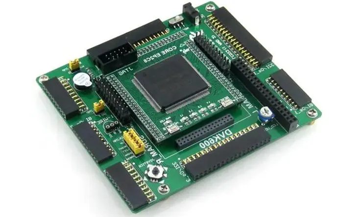
There are several programming languages and tools available for designing FPGAs. Here are some commonly used ones:
● Hardware Description Languages (HDLs): HDLs like Verilog and VHDL are used to create the digital circuit designs that implement the required functions. HDL-based designs are transformed by logic synthesis tools into a netlist of primitive digital logic elements (gates, LUTs, flip-flops, etc.) and connected by logic synthesis tools into a full digital circuit design.
● High-level synthesis (HLS) tools: These tools allow designers to write code in a high-level language such as C/C++, Python or even OpenCL, which is then automatically converted into a hardware description language or a netlist-based design using various optimization criteria. This can significantly reduce design time and provide higher-level abstraction.
● FPGA Development Platforms: FPGA vendors offer development platforms, which include software for design compilation, simulation, synthesis, and debugging. They provide a comprehensive workbench for test and builds utilizing integrated development environments (IDEs).
IP Cores: Intellectual property cores are pre-built blocks of design (i.e. memory, processors, communication interfaces, etc) provided by FPGA vendors to accelerate complex designs or applications development, frequently tailored for specific uses.
● High-Level Design Tools: Commercial high-level tools such as MATLAB, Simulink, or LabVIEW provide integration with FPGA design flows to create and validate designs faster and more efficiently.
The selection of tools and languages may depend on a variety of factors such as the designer’s experience, the complexity of the design, and the specific requirements of the project.
Why an FPGA when a Microcontroller Would Do ?
Choosing between an FPGA and a microcontroller depends on whether the design requires software or hardware functions.
● A microcontroller operates by executing instructions sequentially, which imposes inherent limitations. The intended functionality must align with the available instructions, and performing multiple processing jobs at the same time is generally not feasible. Although instructions are highly flexible and can be executed at high frequencies, software-based digital design still has drawbacks.
● A hardware-based approach is an alternative. Ideally, each new design could be created with a digital IC tailored to the required system functionality. There would be no software development, no instruction set limitations, and no processing delays. The result would be a single IC with input and output pins and digital circuitry designed precisely for the required operations.
● Developing an ASIC for each board is impractical, but FPGAs offer a more practical solution that approximates the process. FPGAs provide the flexibility of reprogrammability to allow digital circuits to be modified to meet specific design requirements. This approach combines the best of both worlds by offering hardware implementation with the flexibility of software-like modifications.
Importance of FPGA
Field-programmable gate arrays (FPGA) are important due to the following reasons:
● Flexibility and Programmability: FPGA offers high flexibility and reprogrammability, which advantages the design of complex digital systems. It is possible to reconfigure the FPGA multiple times, which makes it easy to modify, test, and redesign the system until it satisfactorily meets the requirements. The FPGA’s highly flexible architecture provides an ideal platform for prototyping digital circuits and systems.
● High Performance and Low Power Consumption: FPGAs provide high performance and low power consumption, which makes them suitable for many applications such as, digital signal processing, image, and video processing, artificial intelligence, etc. FPGA provide parallel processing, which improves the computational performance by performing multiple operations at the same time. FPGA design can be optimized for the specific task, reducing the power consumption compared to the general-purpose CPUs.
● Rapid Prototyping: FPGA introduces a faster design and prototyping cycle, and it removes the barriers that traditional ASIC design may possess regarding the time, costs, and effort invested in the design and fabrication of custom chips. FPGA speeds up the prototyping process by delivering an environment that enables designers to implement, validate and upgrade their circuits with no need to have a physical board.
● Hardware Emulation: FPGA is capable of emulating other electronic hardware devices or circuits for testing and debugging purposes eliminating the need for the physical device. It simplifies the test setup, saves research time and further cost, and makes it practical to run tests on complex systems.
Therefore, the FPGA is essential in modern electronics and is increasingly important with the growth of industries such as robotics, IoT, artificial intelligence, and wireless communications. Its customizable and reconfigurable nature makes it suitable for use in research, prototyping, and commercial product development.
Get to More Understand About FPGAs
● The high tooling and pre-production expenses required for custom ASICs make them unsuitable for low to medium scale high-tech products, but they are a great solution for high-volume applications. Instead, for these products, field-programmable gate arrays (FPGAs) are frequently used. These large-scale integrated chips consist of a collection of logic gates, primarily NAND gates, which can be programmed by the manufacturer to carry out a predetermined set of logical operations, meeting specialized requirements.
● PROMs and PLDs were developed in the 1970s and have been succeeded by the current generation of FPGAs. The most notable difference is that FPGAs can be reprogrammed in-circuit by manufacturers, simplifying device management in contrast to pre-programming devices before leaving the factory.
● Modern FPGAs now incorporate analog functionalities, allowing them to integrate more closely with digital functions. These integrations include features such as programmable slew rates, analog-to-digital converters, and differential comparators. This blurring of the lines between FPGAs and Field-Programmable Analog Arrays (FPAAs), which are analog devices, has resulted in the modern FPGAs being capable of analog and digital functions.
FPGA Trends and Future Developments
The trends and future developments in the field of FPGAs include:
● FPGA vs. ASIC: A continued trend is the ongoing competition between FPGAs and ASICs (Application-Specific Integrated Circuits), as both technologies are used for hardware acceleration and optimization. FPGAs offer more flexibility and shorter design cycles, while ASICs offer higher performance and lower power consumption.
● FPGA in the Cloud: Another trend is the use of FPGAs in cloud computing. Cloud providers such as Amazon Web Services, Microsoft Azure, and Alibaba Cloud offer FPGA instances as a service, enabling customers to use FPGAs for various applications without the need for upfront investment in hardware.
● FPGA for AI and Machine Learning: FPGAs offer high parallelism and flexibility, making them well suited for accelerating computationally intensive applications like AI and machine learning. FPGAs can perform tasks such as image and speech recognition, natural language processing, and recommendation systems with high performance and low power.
● Heterogeneous Computing: FPGAs are expected to be more widely used alongside other processing elements such as CPUs and GPUs in heterogeneous computing systems. This allows for the optimization of performance while minimizing energy consumption.
● High-Speed Connectivity: With the growing demand for high-speed connectivity, FPGAs are being used to develop solutions for 5G communications, data centers, and other high-performance networking applications.
● Security: FPGAs have been gaining attention as a potential solution for hardware security. By embedding security mechanisms within the FPGA fabric, it is possible to create secure systems that are resistant to cyber-attacks.
In a word, the demand for FPGAs is expected to continue to grow, as they provide a flexible and powerful tool for hardware acceleration and optimization in a wide range of applications.
Conclusion
Field-Programmable Gate Arrays (FPGAs) are both fascinating and highly effective devices, offering several benefits beyond reducing resource consumption. They can help save significant costs while keeping up with industry developments. Therefore, incorporating FPGAs into a project is a wise decision.
Understanding the fundamental aspects of FPGAs and their advantages over processor-based systems can be beneficial. Designers familiar with microcontrollers, ASICs, and mathematical calculations may initially find modern FPGAs intimidating due to their complexity and high performance. However, enhancing performance and versatility in certain applications may justify the additional design effort required.
In a word, FPGAs provide significant benefits to PCB design engineers. Understanding their features and capabilities can allow designers to make well-informed decisions when selecting digital system components, ultimately leading to developing high-performance and cost-effective electronics solutions.
Related Posts:
1.Land Grid Array (LGA): Advantages, Challenges, Limitations, Applications
2.What is the Integrated Circuit (IC) Board?
3.What Is RFID and Benefits of RFID in PCB Industry?
5.Comprehensive Guide to IC Substrate Design and Manufacturing
