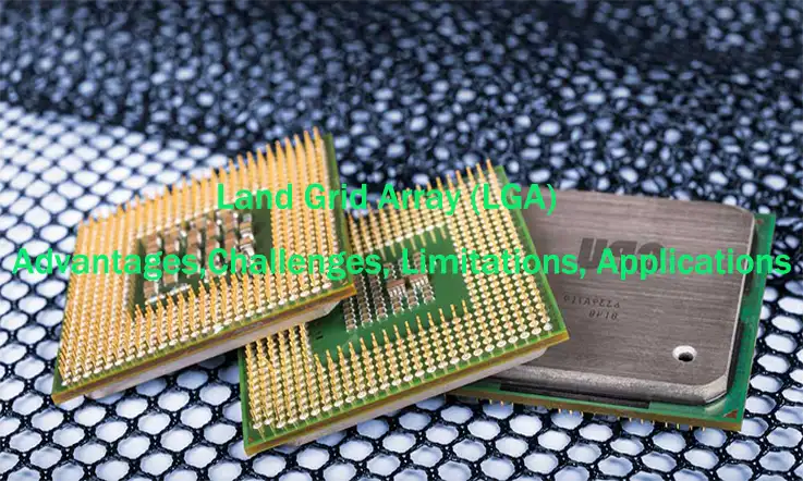
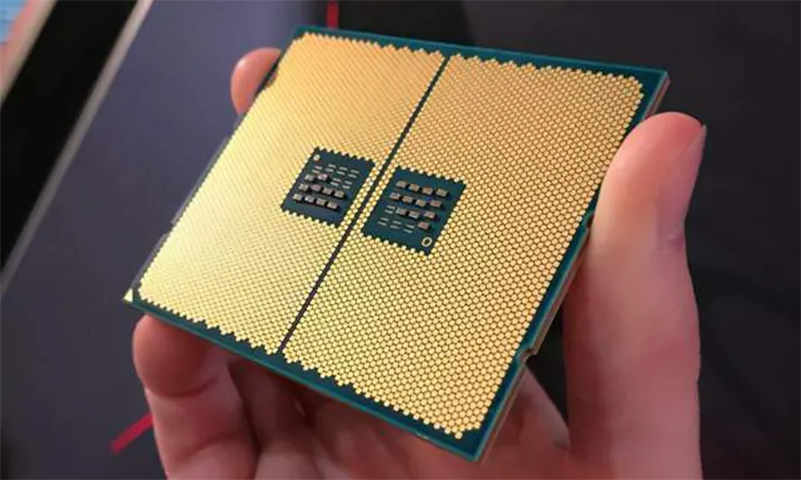
The Land Grid Array (LGA) package is a form of technology comprising lands and an array of grid connections positioned on the inner side of the package. These grid connections serve the purpose of establishing connections on the surface of a Printed Circuit Board (PCB). It is worth noting that not all columns and rows of the grid need to be utilized, as the LGA socket or solder paste can facilitate the creation of connections. The elements within the grid exhibit diverse shapes and sizes, including polygonal, triangular, circular, and honeycomb patterns. The specific design may be influenced by factors such as the electrical gap between adjacent contacts and the likelihood of contact, rather than focusing solely on tolerances. Consequently, this approach leads to the creation of optimal shapes and forms for the spring contacts of the counterpart, ensuring effective connectivity for outgoing electricity to a backplane PCB.
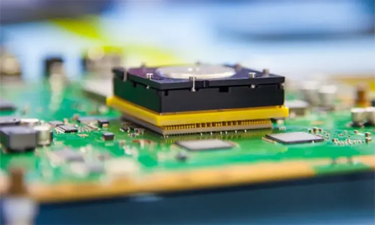
The LGA packaging technology is closely associated with Pin Grid Array (PGA) and Ball Grid Array (BGA) packaging methods. However, unlike PGA, LGA packages are designed to be soldered down using Surface-mounted Technology (SMT) or fit into a socket.
Furthermore, LGA packages do not incorporate solder balls or sockets. Instead, they utilize flat connection pins that are directly placed on the PCB. In contrast, BGA packages do feature solder balls as connection pins between Integrated Circuits (ICs) and Printed Circuit Boards. These solder balls are positioned beneath the IC.
Why Use LGA (Land Grid Array)?
There are several Advantages why LGA (Land Grid Array) technology is used in electronic packaging:
Improved Electrical Performance
LGA packaging offers several benefits for electrical performance. The shorter electrical paths between the integrated circuit (IC) and the printed circuit board (PCB) result in reduced signal noise and crosstalk. This leads to improved signal integrity and higher data transfer rates. LGA packaging also exhibits lower inductance and capacitance, minimizing the impact on high-frequency signals and enabling better overall electrical performance.
Enhanced Thermal Management
LGA packaging provides efficient heat dissipation from the IC to the PCB. The large surface area of the metal lands allows for effective heat transfer, helping to keep the IC cool during operation. This is particularly important for power-hungry ICs or devices that generate significant heat. Effective thermal management contributes to the longevity and reliability of the IC and helps prevent thermal-related issues.
Mechanical Stability and Reliability
LGA packaging offers a robust and secure connection between the IC and the PCB. The direct attachment of the IC to the lands provides mechanical stability, making it resistant to mechanical stresses, vibrations, and shocks. This reduces the risk of damage or disconnection, contributing to the long-term reliability of the electronic device. LGA packaging is also less susceptible to solder joint failures compared to other packaging types, enhancing its overall reliability.
Higher Pin Density
LGA packaging allows for a higher density of pins or contacts compared to other packaging technologies. The lands on the package provide a larger area for placing electrical contacts, enabling a greater number of connections between the IC and the PCB. This increased pin density enables the integration of more functionality and features into a smaller footprint, making LGA packaging suitable for applications with space limitations.
Ease of Automated Assembly
LGA packaging is well-suited for automated assembly processes. The standardized layout of the lands and the use of solder balls or bumps for attachment facilitate efficient and precise assembly. The consistent design enables automated pick-and-place machines to accurately position the IC on the PCB. The simplified assembly process and compatibility with automated manufacturing contribute to improved production efficiency and reduced costs.
Compatibility with Advanced Technologies
LGA packaging is compatible with various advanced technologies and manufacturing processes. It can accommodate fine pitch requirements, high-speed signaling, and advanced packaging techniques such as flip-chip bonding. This makes LGA packaging suitable for a wide range of applications, including high-performance computing, telecommunications, and consumer electronics.
Overall, LGA packaging offers improved electrical performance, efficient thermal management, mechanical stability, higher pin density, and compatibility with advanced technologies. These advantages make LGA packaging a preferred choice for applications that require high reliability, miniaturization, and high-speed performance.
Challenges and Limitations of LGA Packaging
While LGA packaging offers several advantages, it also has some challenges and limitations that need to be considered. These include:
Cost: LGA packaging can be more expensive compared to other packaging types, such as pin grid array (PGA) or quad flat package (QFP). The additional complexity in manufacturing, including the use of solder balls or bumps, can contribute to higher production costs.
Socket Design: The design and construction of LGA sockets can be more intricate compared to other socket types. The socket needs to provide proper alignment, secure retention, and reliable electrical connections. Ensuring the long-term durability and reliability of the socket can be a challenge.
Socket Wear and Damage: Over time, repeated insertions and removals of LGA packages can cause wear and damage to the socket contacts. This can lead to reduced electrical connectivity, increased contact resistance, and potential reliability issues. Regular maintenance and replacement of sockets may be necessary in high-use scenarios.
Inspection and Rework: LGA packages can be challenging to inspect and rework due to the surface-mount nature of the packaging. Visual inspection of solder joints and detection of defects can be more difficult compared to traditional through-hole packages. Reworking or repairing LGA packages may require specialized equipment and skilled operators.
Package Size and Pitch: As LGA packages offer higher pin densities, the package size and pitch (spacing between the pins) can become smaller. This can pose challenges in terms of manufacturing tolerances, PCB design, and assembly processes. Fine-pitch LGA packages may require advanced manufacturing techniques and stricter quality control measures.
Thermal Considerations: While LGA packaging offers good thermal management, the dissipation of heat from the IC to the PCB can still be a concern, especially for high-power devices. Proper thermal design, including the use of heat sinks or thermal vias, is crucial to prevent overheating and ensure reliable operation.
Limited Component Accessibility: Once an LGA package is soldered to the PCB, accessing and replacing the IC becomes more challenging compared to socketed packages. This can pose difficulties in cases where the IC needs to be upgraded or repaired.
Compatibility and Standardization: LGA packaging comes in various configurations and socket designs, which may not be compatible across different manufacturers or generations. Ensuring compatibility and standardization can be a challenge when integrating LGA packages from different sources or when upgrading components.
Despite these challenges, LGA packaging continues to be widely used due to its advantages in terms of electrical performance, thermal management, and mechanical stability. Manufacturers and designers need to carefully consider these limitations and implement appropriate measures to mitigate any potential issues.
LGA Applications
LGA (Land Grid Array) packaging finds applications in various industries and devices. Here are some common examples of LGA applications:
Computer Processors (CPUs):
● LGA packaging is widely used in computer processors, such as Intel Core i7, i5, and i3 series.
● It provides a high pin density, allowing efficient electrical connectivity and thermal management.
Chipsets:
● LGA packaging is commonly used for chipsets, which are integrated circuits that manage the communication between various components in a computer system.
● Chipsets play a crucial role in controlling data flow and enhancing system performance.
Graphics Cards:
● High-performance graphics cards, used in gaming and professional applications, often utilize LGA packaging.
● LGA enables efficient power delivery, reliable signal transmission, and effective heat dissipation for graphics processing units (GPUs).
Network Equipment:
● LGA packaging is employed in network equipment, such as routers, switches, and network interface cards (NICs).
● These devices require high-speed data processing, low latency, and reliable connectivity, which LGA packaging can provide.
Industrial Control Systems:
● LGA packaging is utilized in industrial control systems, including Programmable Logic Controllers (PLCs) and automation equipment.
● These systems require robust and reliable connections to handle various input/output signals and control processes.
Automotive Electronics:
● LGA packaging is increasingly used in automotive electronics, including engine control units (ECUs), infotainment systems, and advanced driver-assistance systems (ADAS).
● LGA offers durability and secure connections, ensuring stable operation in harsh automotive environments.
Consumer Electronics:
● LGA packaging is found in various consumer electronic devices, such as smartphones, tablets, and laptops.
● It enables compact designs, efficient power delivery, and reliable connections for the integration of processors, memory modules, and other components.
Medical Devices:
● LGA packaging is utilized in medical devices like diagnostic equipment, patient monitoring systems, and medical imaging devices.
● It ensures accurate data processing, reliable connectivity, and resistance to environmental factors.
These are just a few examples of LGA applications, and the technology continues to find use in a wide range of electronic devices where high performance, reliability, and efficient thermal management are required.
LGA (Land Grid Array) Vs. PGA: Which Is Better?
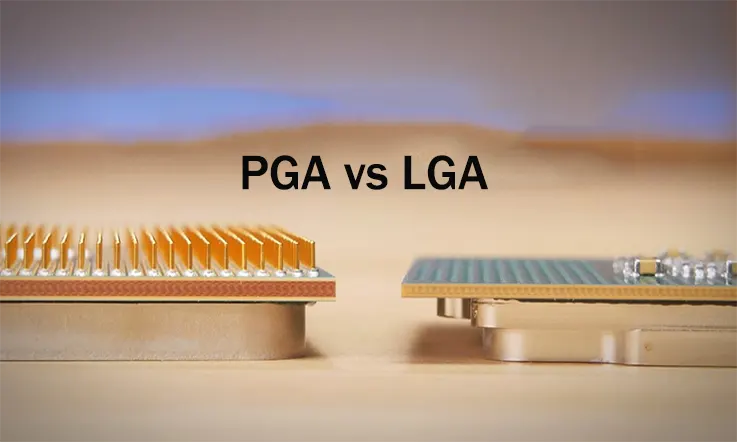
Determining which is better between LGA (Land Grid Array) and PGA (Pin Grid Array) depends on various factors and specific application requirements. Here are some considerations to help you make an informed decision:
Pin Density and I/O Requirements: LGA packages typically offer higher pin densities compared to PGA packages. If your application requires a higher number of input/output (I/O) connections or demands a higher pin count, LGA might be more suitable.
Thermal Considerations: Both LGA and PGA packages can handle heat dissipation effectively, but the thermal characteristics differ. LGA packages have a larger contact area with the PCB, which facilitates better thermal conductivity. If your application involves components generating significant heat, LGA may provide better thermal management capabilities.
Manufacturing and Assembly Requirements: LGA packages have flat contact pins that are soldered directly onto the PCB or inserted into a socket. This makes them easier to assemble and replace, especially in socketed applications. PGA packages, on the other hand, have pins that are inserted into holes in the PCB, requiring through-hole soldering techniques. PGA assembly may be more time-consuming and complex.
Mechanical Stability and Reliability: LGA packages offer a robust mechanical connection due to their larger contact area and multiple pins. This makes them more resistant to mechanical stress, such as vibrations and shocks. PGA packages, with their pins inserted into holes, also provide reliable connections but may be less robust in high-stress environments.
Cost Considerations: The cost of LGA and PGA packages can vary depending on factors such as pin count, package size, and manufacturing complexity. In general, LGA packages may have a slight advantage in terms of lower manufacturing costs due to their simpler assembly process.
It is crucial to evaluate these factors in the context of your specific application requirements, such as pin count, thermal management needs, manufacturing considerations, mechanical stability, and cost constraints. Consulting with your design and manufacturing teams or engaging with component suppliers can provide valuable insights to determine whether LGA or PGA is better suited for your particular application.
LGA (Land Grid Array) Vs. BGA: Which SMT Should You Use?
The choice between LGA (Land Grid Array) and BGA (Ball Grid Array) surface-mount technologies depends on several factors and considerations specific to the application requirements and design constraints. Here are some points to help you decide:
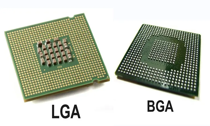
Pin density and I/O requirements: LGA packages typically offer higher pin densities compared to BGA packages. If your application requires a higher number of input/output (I/O) connections or demands a higher pin count, LGA may be a more suitable choice.
Thermal considerations: Both LGA and BGA packages can handle heat dissipation effectively, but the thermal characteristics differ. LGA packages have a larger contact area with the PCB, which facilitates better thermal conductivity. If your application involves components generating significant heat, LGA may provide better thermal management capabilities. BGA packages, on the other hand, have solder balls that can act as additional heat pathways, dispersing heat more evenly across the package.
Manufacturing and assembly requirements: LGA packages have flat contact pins that are soldered directly onto the PCB or inserted into a socket. This makes them easier to assemble and replace, especially in socketed applications. BGA packages, with their solder balls, require precise alignment and reflow soldering techniques, which may be more complex and costly during assembly.
Mechanical stability and reliability: LGA packages offer a robust mechanical connection due to the larger contact area and multiple pins. This makes them more resistant to mechanical stress, such as vibrations and shocks. BGA packages, with their solder balls acting as connections, can also provide reliable connections, but they may be more susceptible to mechanical failures if subjected to excessive stress.
Cost considerations: The cost of LGA and BGA packages can vary depending on factors such as pin count, package size, and manufacturing complexity. In general, LGA packages may have a slight advantage in terms of lower manufacturing costs, as they do not require the precise ball alignment and reflow soldering processes associated with BGA packages.
It is essential to evaluate these factors in the context of your specific application requirements, such as I/O demands, thermal management needs, manufacturing considerations, mechanical stability, and cost constraints. Consulting with your design and manufacturing teams or engaging with component suppliers can provide valuable insights and help you make an informed decision on whether to use LGA or BGA surface-mount technology.
In Conclusion
LGA (Land Grid Array) packaging is a popular technology used in electronic devices for connecting integrated circuits (ICs) to printed circuit boards (PCBs). It offers several advantages, including improved electrical performance, efficient thermal management, enhanced mechanical stability, higher pin density, and ease of automated assembly. These benefits make LGA packaging well-suited for a wide range of applications in various industries.
However, LGA packaging also has its challenges and limitations. These include higher costs, intricate socket designs, potential wear and damage to sockets, inspection and rework difficulties, size and pitch concerns, thermal considerations, limited component accessibility, and compatibility issues. These factors need to be carefully addressed and managed to ensure the successful implementation of LGA packaging.
Despite these challenges, LGA packaging continues to evolve and improve, driven by advancements in technology and the demand for higher performance and miniaturization. Ongoing research and development efforts aim to overcome the limitations and further enhance the benefits of LGA packaging.
Overall, LGA packaging remains a valuable packaging solution that enables the integration of advanced ICs into electronic devices, contributing to improved functionality, reliability, and performance. It is important for manufacturers, designers, and engineers to carefully evaluate the specific requirements of their applications and consider the benefits and challenges associated with LGA packaging to make informed decisions and achieve optimal results.
In addition, if you want LGA technology in your IC, then contact JarnisTech now.
Related Posts:
2.What is the Integrated Circuit (IC) Board?
3.What Is RFID and Benefits of RFID in PCB Industry?
4.What Is FPGA and Why Do You Need to Care?
5.Comprehensive Guide to IC Substrate Design and Manufacturing