Substrate-like PCBs (SLPs) have emerged as a game-changing technology in the field of PCB design and manufacturing. With their unique characteristics and capabilities, SLPs are transforming the industry by enabling smaller chipsets, accommodating more components in limited space, and offering faster production cycles.
What Is SLP?
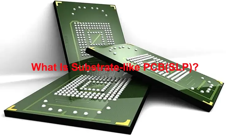
Substrate-like PCB (SLP) is essentially a high-end HDI board. From a manufacturing perspective, SLP is more similar to IC substrates used in semiconductor packaging, but it has not yet reached the level of IC substrates in terms of specifications. The core competitive advantage of SLP lies in the integration of board technology and HDI technology, which is reflected in the optimization capability of equipment and production lines, yield rate, and cost control. Its main difference from ordinary HDI lies in the minimum line width and spacing and the manufacturing process (mSAP – semi-additive process). SLP can be considered as an any-layer HDI board (interconnections on any layer) using the mSAP method.
Where Are Substrate-Like PCBs Used?
Substrate-like PCBs have emerged as a significant driving force in the PCB industry, primarily due to the rapid growth of the mobile device market. The continuous advancements in tablet, smartphone, and wearable technologies have necessitated more sophisticated device constructions and internal PCB designs. This trend has led to the development of smaller chipsets, allowing for the integration of an increasing number of features within a limited space. Furthermore, the demand for sleeker enclosures and larger batteries has compelled manufacturers to reduce the size of the PCBs.
A notable illustration of this trend can be observed in the recent implementations by industry giants Samsung and Apple. These companies have successfully incorporated substrate-like PCBs with linewidth/spacing dimensions of 25/25 μm and 30/30 μm in their devices. By employing these advanced PCBs, smartphones can now accommodate twice as many electronic components compared to traditional HDI boards within the same spatial constraints. This achievement is primarily attributed to the smaller linewidth of substrate-like PCBs. Additionally, the components utilized in these devices have become increasingly diminutive, with simpler components and chips now available in highly compact fine pitch BGAs packages.
Another noteworthy development is the integration of System-on-Chips (SoCs) within these devices. These SoCs are not only capable of performing multiple functions but also possess higher I/O density. Consequently, the need for numerous peripheral components that were traditionally present in such devices has been eliminated. It is worth mentioning that prominent Chinese smartphone manufacturers, including Oppo, Huawei, and Xiaomi, are expected to follow suit and adopt substrate-like PCBs in their product offerings.
The adoption of substrate-like PCBs in the mobile device market has revolutionized the PCB industry. The ability to accommodate more components in a smaller area, coupled with the integration of advanced chipsets, has paved the way for enhanced device capabilities and improved user experiences. As the market continues to evolve, we can anticipate further advancements and wider adoption of substrate-like PCB technology across various electronic devices.
SLP Manufacturing Technology
Currently, there are three main process technologies used in printed circuit board (PCB) and substrate manufacturing: subtractive process, additive process, and semi-additive process.
Subtractive Process:
The subtractive process is the earliest and most mature manufacturing technique for PCBs. It typically involves using photosensitive etching materials to transfer the circuit pattern and protect the areas that do not need to be etched. Then, an acid or alkaline etching solution is used to remove the unprotected copper layer.
Additive Process (SAP):
The additive process involves using an insulating substrate with photosensitive catalyst. After exposing the substrate to the circuit pattern, selective chemical copper deposition is used to create the conductor pattern.
Semi-Additive Process (MSAP):
The semi-additive process addresses the challenges of both subtractive and additive processes in creating fine circuit patterns. In this process, a chemical copper layer is formed on the substrate and a resist pattern is created on top. Through electroplating, the resist pattern is thickened and then removed. The excess chemical copper layer is removed using flash etching. The areas that were not thickened due to the resist protection are quickly removed during differential etching, leaving behind the desired circuit pattern.
Although SLP belongs to the category of printed circuit boards, its fine line width and spacing of 20μm/35μm cannot be produced using the subtractive process. Therefore, MSAP process technology is also required for SLP production.
SLP Tech vs. Standard PCB & IC Substrate: Differences
Substrate-like PCBs (SLPs) offer a fast and efficient solution for PCB fabricators to enable system designers to bring their systems to market quickly and with high yields. This is achieved through a carefully designed process that takes into account various critical factors, including component type, geometry, die-substrate mismatch, assembly steps, temperature ramp-up, cleaning, and electrical tests. These production details are often challenging for designers to anticipate and incorporate into their initial designs.
To illustrate this, consider the scenario where the power density (W/mm2) is excessively high, leading to the need for effective heat dissipation. In such cases, system engineers typically employ active dissipation devices to extract excessive heat from sensitive components. However, when collaborating with PCB design engineers to build an SLP, advanced heat dissipation techniques can be utilized. For instance, embedded coins with low coefficient of thermal expansion (CTE) can be incorporated into the SLP design. These coins efficiently pull heat from the components and direct it into a heat sink, reducing the reliance on additional active cooling systems such as fans, cooling fins, or cooling pipes. This not only saves costs but also conserves valuable space that would otherwise be occupied by these supplementary cooling devices. It is important to note that while heat dissipation is a critical step, it is not the sole focus of the SLP design process.
Therefore, traditional PCB designs rarely account for Chip-on-Board (CoB) and die cavity configurations. However, IC substrates, such as SLPs, are specifically designed to accommodate these specialized requirements, often deviating from the design considerations of regular surface mount device (SMD) components. By leveraging the advantages of SLP technology, PCB fabricators can streamline the design and manufacturing process, enabling system designers to introduce their systems to the market swiftly and with confidence in achieving high yields.
SLP Technology: High-Frequency/Speed Compatible?
Yes, SLP technology is well-suited for high-frequency or high-speed applications. The design and construction of substrate-like PCBs take into consideration various factors that are crucial for achieving optimal performance in these applications.
SLPs offer several advantages that make them suitable for high-frequency or high-speed applications. Firstly, the smaller dimensions and reduced parasitic effects of SLPs contribute to improved signal integrity and reduced signal loss, enabling higher-frequency operation. The smaller linewidth/spacing dimensions in SLPs allow for tighter trace routing and reduced crosstalk, which is particularly important in high-speed designs.
Additionally, SLPs provide enhanced thermal management capabilities, which are critical for high-frequency or high-speed applications that generate significant heat. The use of advanced heat dissipation techniques, such as embedded coins with low CTE, helps efficiently dissipate heat from components, preventing thermal issues that can degrade performance.
Furthermore, SLPs can be designed to accommodate specific requirements for impedance control, signal integrity, and transmission line characteristics. This ensures that high-frequency signals propagate effectively and minimize signal degradation.
It’s worth noting that the suitability of SLP technology for high-frequency or high-speed applications also depends on other factors such as the specific design requirements, materials used, and manufacturing processes employed. However, overall, SLPs offer a viable and efficient solution for achieving optimal performance in such applications.
Substrate-like PCB(SLP): System Reliability Impact?
When designing a system, it is crucial to carefully consider the Coefficient of Thermal Expansion (CTE) mismatch between the PCB, IC substrate, and die. The CTE mismatch can lead to reliability issues and performance degradation. However, Substrate-like PCBs (SLPs) provide a solution that effectively bridges the CTE gap between the PCB and IC substrate, resulting in significant benefits such as cost reduction and shorter production times.
By utilizing SLP technology, the CTE mismatch is minimized, ensuring better thermal stability and reliability of the system. SLPs are specifically engineered to have a CTE that closely matches that of the IC substrate and die. This compatibility reduces the stress and strain caused by temperature variations during operation, mitigating the risk of solder joint failures and other reliability concerns.
The ability of SLPs to bridge the CTE gap brings about notable advantages. Firstly, it lowers costs by reducing the need for additional measures to address the CTE mismatch, such as specialized materials or complex assembly processes. The compatibility between the PCB and IC substrate simplifies the manufacturing process and eliminates potential sources of failure, resulting in cost savings.
Secondly, SLPs contribute to shorter production times. The elimination of complex CTE compensation techniques streamlines the manufacturing process and allows for faster production cycles. This accelerated timeline enables system designers to bring their products to market more quickly, gaining a competitive edge.
All in all, SLPs offer a solution that effectively addresses the CTE mismatch between the PCB, IC substrate, and die. By bridging this gap, SLPs enhance thermal stability, reduce costs associated with CTE compensation, and expedite production times. System designers can benefit from the improved reliability and efficiency provided by SLP technology, enabling them to deliver high-quality products in a timely and cost-effective manner.
How SLP Technology Overcoming High Power Overheating?
Thermal management is an increasingly critical concern in both bare PCB and assembly levels, particularly in high-power and high-voltage applications. To address the need for improved heat transfer and cooling solutions, the adoption of copper coin inserts, often made of Copper Molybdenum Copper (CMC), has become common.
The copper coin heat dissipation method involves the integration of a solid copper piece onto or into the PCB, typically positioned beneath specific component(s) that require effective cooling. Compared to a via farm, the copper coin offers approximately ten times better cooling performance. By establishing direct contact between the heat-generating component pad and the heat sink, the copper coin facilitates efficient heat transfer without relying on thermally conductive materials.
Copper coin technology is particularly suitable for scenarios where one or a few components on the PCB generate significant heat. It provides an optimal heat transfer solution in a localized manner, regardless of the number of PCB layers or the chosen PCB material. Moreover, the adoption of copper coins significantly reduces the weight of the substrate when compared to traditional heat sinks or active cooling elements.
Summary
Substrate-like PCBs (SLPs) have revolutionized the PCB industry by bridging the gap between traditional PCB designs and IC substrates. By minimizing the Coefficient of Thermal Expansion (CTE) mismatch, SLPs ensure better thermal stability and reliability of systems, while reducing costs and production time. The integration of copper coin inserts further enhances thermal management, making SLPs ideal for high-power and high-voltage applications.
As Chinese manufacturers follow the footsteps of industry leaders like Samsung and Apple, the adoption of SLP technology is expected to increase. With improved signal integrity, reduced signal loss, and enhanced thermal management, SLPs pave the way for more efficient and compact electronic systems. The era of Substrate-like PCBs has arrived, promising a future of advanced PCB designs and accelerated innovation.
Related Posts:
1.Land Grid Array (LGA): Advantages, Challenges, Limitations, Applications
3.What Is RFID and Benefits of RFID in PCB Industry?
4.What Is FPGA and Why Do You Need to Care?
5.What is the Integrated Circuit (IC) Board?
6.Comprehensive Guide to IC Substrate Design and Manufacturing