The assembly of electronic circuits via Surface Mount Technology (SMT) demands a profound understanding of materials science and process control. This text provides a systematic framework for professionals seeking to achieve high-yield, high-reliability solder connections. It moves from foundational principles to advanced process optimization, establishing a comprehensive guide to modern SMD soldering.
The Unchanging Foundation: Physics and Chemistry of the Solder Joint
A dependable solder joint originates from the application of fundamental physical and chemical laws. A command of these principles is a prerequisite for effective process control and troubleshooting, moving beyond procedural execution to achieve predictable, high-caliber results.
Wetting and Surface Tension
The formation of a solder joint relies on the principle of wetting: the ability of molten solder to spread across a solid surface, such as a PCB pad or component lead. This behavior stems from the interplay between the solder’s internal cohesive forces and the adhesive forces between the solder and the metallic surface. For a sound connection, adhesive forces must prevail, enabling the solder to flow and form a broad, smooth contact area.
●Contact Angle: This measurement gauges wetting effectiveness. A low contact angle signifies thorough wetting and a strong bond, whereas a high contact angle points to poor wetting and a probable joint defect.
●Surface Tension: An inherent property of liquids, surface tension causes molten solder to pull inward into a spherical shape. The soldering process, particularly the chemical action of flux, is engineered to reduce this tension, promoting the required spread and flow.
Formation of the Intermetallic Compound (IMC) Layer
A solder joint is a metallurgical connection created by an Intermetallic Compound (IMC) layer. This distinct alloy forms at the interface when molten solder reacts chemically with the copper (Cu) of the PCB pad and the component termination. This layer, typically just a few microns thick, provides the joint’s structural integrity and electrical continuity.
●Proper IMC Formation: A thin, uniform IMC layer (such as Cu₆Sn₅ and Cu₃Sn) is the objective for a durable, long-lasting connection.
●Risks of Excessive Growth: Extended soldering time or elevated temperatures can cause this layer to thicken. An overly thick IMC layer becomes brittle, making the joint susceptible to fracture under mechanical or thermal stress. Managing IMC growth is a primary goal of thermal profile optimization.
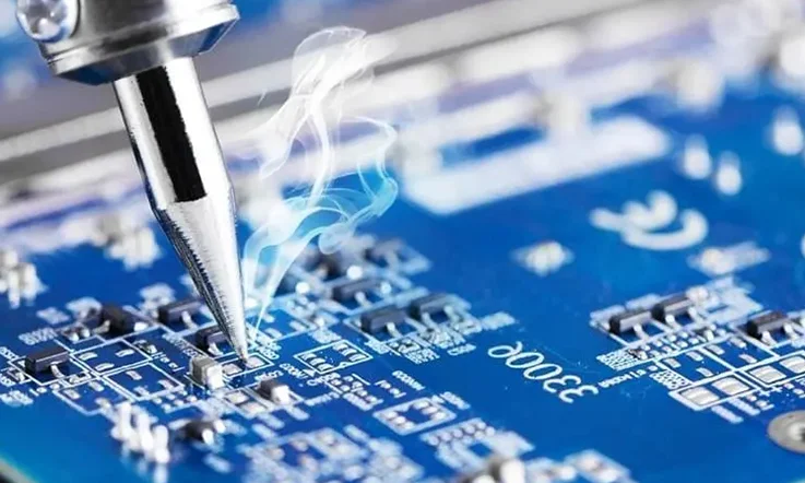
The Function of Flux in Oxide Removal
Metallic surfaces, particularly copper, naturally develop a thin oxide layer when exposed to air. This non-wettable film obstructs the molten solder, preventing a proper metallurgical bond. Flux is formulated to chemically remove these oxides immediately before and during soldering.
●Surface Cleaning: Flux contains activators, such as mild organic acids, that become reactive at soldering temperatures. As the assembly heats, the flux melts and its activators cleanse the metal oxides from the surfaces.
●Oxidation Prevention: After cleaning, the liquid flux covers the pristine metal. This temporary shield prevents re-oxidation in the hot, oxygen-filled environment of the reflow oven, leaving a clean surface available for the solder to bond with.
Precise management of these chemical and physical interactions is what separates a standard assembly from a high-reliability electronic product.
Process Control in the SMT Workflow
The Surface-Mount Technology (SMT) production line is a sequence of interdependent stages. A deviation in an early stage propagates through the workflow, affecting the final assembly’s quality. Effective process control, therefore, extends beyond task execution to include the monitoring and verification of each stage’s output with quantitative data.
Stencil Printing: Accurate Paste Deposition
The stencil printing stage establishes the groundwork for the final solder joints. The objective here is the deposition of a precise and repeatable volume of solder paste onto every land pattern. The accuracy of this deposit directly influences defect rates for conditions such as bridging, opens, and insufficient solder.
●Stencil Fabrication: The stencil’s aperture design (dimensions and shape) and foil thickness collectively define the theoretical print volume. For fine-pitch components, stencils are fabricated using laser cutting and electropolishing to enhance paste transfer efficiency.
●Squeegee Mechanics: The squeegee’s pressure, speed, and angle of attack are calibrated to fill apertures completely without causing paste to scoop or smear, ensuring a clean print.
●3D SPI Verification: A 3D Solder Paste Inspection (SPI) system is integrated immediately after printing. This apparatus measures the volume, area, and height of every paste deposit, supplying immediate process feedback and preventing boards with printing defects from proceeding.
Component Placement: Positional and Force Precision
Following paste deposition, the assembly moves to automated component placement. Machines pick individual components, use vision systems to check identity and orientation, and then place them onto the corresponding pads.
●Placement Accuracy: The system must achieve high repeatable accuracy, often within ±25 µm, to correctly position fine-pitch packages like BGAs and 0201 components.
●Placement Force: The machine’s Z-axis applies a calibrated force to set the component securely into the paste without squeezing paste out from under the component body, which would cause bridging.
●Vision System: The integrated vision system serves a dual purpose: it aligns the component for placement and can identify parts with bent leads or other physical defects before they are mounted.
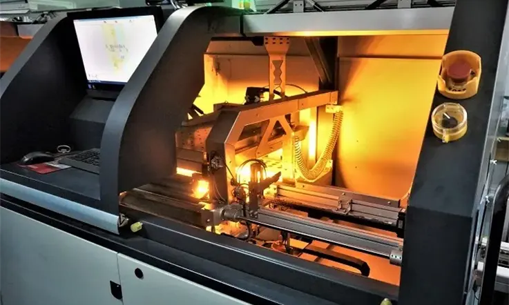
Reflow Oven Thermal Profiling
Once components are placed, the assembly enters the reflow oven where the solder joints are formed. This is not a passive heating step; it is a tightly controlled thermal process. A specific temperature-versus-time profile is developed for each assembly. This profile guides the PCB through several zones—preheat, soak, reflow, and cooling—to melt the solder paste and create a sound metallurgical bond without subjecting the components or the board to excessive thermal stress.
Post-Reflow Inspection: Automated Verification
After the assembly exits the reflow oven, a verification step confirms the process quality. This procedure is designed not merely to find defects, but to gather data that helps keep the manufacturing process centered and stable.
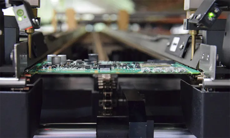
●Automated Optical Inspection (AOI): This high-speed, non-contact method employs cameras to examine the PCB surface. It is highly effective at detecting visible anomalies like missing components, incorrect polarity, solder bridging, and insufficient solder.
●Automated X-ray Inspection (AXI): This method is applied to components with hidden solder joints, such as Ball Grid Arrays (BGAs). X-rays penetrate the component, generating an image of the underlying connections to check for shorts, opens, voids, and other concealed defects.
Thermal Profile Optimization in Reflow Soldering
The reflow oven facilitates the transformation of solder paste into a solid metallurgical connection. This transformation is governed by the thermal profile—the precise temperature sequence an assembly experiences over time. Engineering a correct profile is a demanding aspect of SMT assembly, requiring a balance between the thermal needs of diverse components and materials on a single board.
The Four Zones of a Reflow Profile
A standard reflow profile is segmented into four distinct zones, each with a specific thermodynamic function. Successful passage through each zone prepares the assembly for the next.
1. Preheat Zone: The assembly undergoes a controlled, linear temperature rise (typically 1–3°C per second). This gradual ramp prevents thermal shock to components and allows volatile solvents in the solder paste to outgas safely.
2. Soak Zone: The temperature is held at a constant plateau (e.g., 150–200°C) for 60–120 seconds. This stage allows the temperature to equalize across the entire board, minimizing temperature differentials (ΔT) and ensuring the flux is fully activated before reflow.
3. Reflow Zone: The temperature is rapidly increased past the solder’s liquidus point. The duration that the assembly spends above this point, or Time Above Liquidus (TAL), is typically 30–90 seconds. This allows the solder to melt, wet the component and pad surfaces, and form the intermetallic (IMC) layer.
4. Cooling Zone: The final stage is a controlled cooling ramp (e.g., -2 to -4°C per second). A carefully managed cooling rate promotes the formation of a fine-grain microstructure in the solder, which yields superior mechanical strength and prevents the growth of thick, brittle IMC layers.
| Zone | Function | Typical Temperature / Rate | Typical Duration |
| Preheat Zone | Controlled temperature ramp to avoid thermal shock, allow solvent outgassing | 1–3 °C/sec ramp to ~150°C | 60–120 sec |
| Soak Zone | Equalize board temperature, activate flux | 150–200°C plateau | 60–120 sec |
| Reflow Zone | Melt solder, wet surfaces, form IMC | Peak 235–250°C, TAL 30–90 sec | 30–90 sec above liquidus |
| Cooling Zone | Control cooling to refine solder microstructure, prevent brittle IMC growth | -2 to -4 °C/sec cooling rate | Until < 100°C |
Profiling Strategies for Complex Assemblies
A generic profile is inadequate for complex circuit boards. Assemblies with a high mix of component sizes, large copper planes, or high overall thermal mass present a challenge to achieving temperature uniformity.
●Profile Adjustment: For such boards, a profile with a pronounced soak plateau is generally selected. This provides the necessary time for large components to reach the same temperature as smaller parts. Thermocouples are attached to the board at various locations to measure the actual temperature profile as it passes through the oven. The oven’s zone setpoints are then iteratively adjusted until the measured profile falls within the desired process window.
●Process Window Index (PWI): To quantify the profile’s robustness, the Process Window Index (PWI) is calculated. This metric statistically measures how well the profile fits within the specifications of the solder paste and components. A PWI below 100% indicates a capable and centered process.
| Parameter | Typical Range / Example | Purpose |
| Soak Plateau Temperature | 150–200°C | Equalizes large & small component temperature |
| Soak Duration | 60–120 sec | Allows flux activation & ΔT reduction |
| Number of Thermocouples | 3–5+ (varied board positions) | Measure actual temperature at critical points |
| PWI Target | < 100% | Ensures process is within solder/component limits |
The Utility of Vacuum Reflow Technology
Void formation within solder joints is a persistent defect that can compromise a product’s thermal and mechanical durability. Vacuum reflow soldering is an advanced process engineered to address this issue.
●Process: In a vacuum reflow system, after the solder becomes molten, the process chamber is subjected to a partial vacuum.
●Mechanism: This reduction in ambient pressure allows any trapped gas bubbles—originating from flux volatiles—to expand and escape from the liquid solder.
●Result: This technology substantially reduces void percentages in solder joints. This level of performance is frequently a requirement for high-reliability assemblies in the automotive, aerospace, and medical fields.
Assembly Methodologies for Advanced Component Packages
The progression toward smaller and more powerful electronics relies on the adoption of advanced component packages. These packages, while enabling superior density and performance, have specific design characteristics that demand specialized knowledge and refined assembly techniques.
Soldering Considerations for BGA and CSP
Ball Grid Array (BGA) and Chip Scale Packages (CSP) feature connections on the component’s underside, making both assembly and inspection complex. A successful outcome depends on precise solder paste deposition and diligent warpage control.
●Paste Volume Control: The stencil printing process is engineered to deposit a precise volume of solder paste onto each pad, with the accuracy of every deposit verified by 3D Solder Paste Inspection (SPI).
●Warpage Mitigation: A carefully developed thermal profile, often featuring a slow ramp rate and an extended soak phase, minimizes the thermal gradients across the board and package that can induce warpage.
●Post-Reflow Inspection: After assembly, 3D Automated X-ray Inspection (AXI) is the definitive method for examining internal features, including voids, shorts, and the subtle Head-in-Pillow (HiP) defect.
●Underfill Application: For applications requiring enhanced mechanical durability, an underfill epoxy can be dispensed beneath the component after reflow. This process reinforces the solder joints, improving their resilience to shock and vibration.
Managing the Thermal Pad on QFN and DFN Packages
Quad Flat No-lead (QFN) and Dual Flat No-lead (DFN) packages are selected for their excellent thermal dissipation, facilitated by a large, exposed pad on their underside. This feature, however, introduces a common soldering challenge.
●The Defect Mechanism: Applying a single, large solder paste deposit to the thermal pad can trap significant voiding. It can also cause the lightweight component to float on the surface of the molten solder, preventing its perimeter I/O pads from making proper contact with the PCB.
●The Stencil Solution: A “window-pane” or “checkerboard” aperture design is implemented in the stencil. This strategy divides the single large deposit into multiple smaller ones. This approach provides outgassing channels for flux volatiles to escape and reduces the net surface tension, allowing the component to seat correctly.
Assembly of 0201 and 01005 Passive Components
The assembly of ultra-small passive components, such as those in the 0201 and 01005 footprints, requires process control at its most stringent. At this scale, minute process variations can result in defects.
●Printing Materials: A thin stencil foil (e.g., 75-100 microns) combined with a fine-particle solder powder (Type 5 or smaller) is used to accurately print the minuscule solder deposits.
●Placement Mechanics: The placement equipment must offer exceptional positional accuracy and apply a minimal placement force to avoid disturbing the paste or damaging these fragile components.
●Defect Prevention: The “tombstoning” defect, where a component stands on one end, is a frequent issue. It is effectively prevented through symmetrical PCB pad design and a highly uniform thermal process during reflow.
Techniques for Package-on-Package (PoP) Assembly
Package-on-Package (PoP) technology, which involves stacking components like a processor on top of a memory module, represents a further step in three-dimensional integration. This assembly process requires managing the complexities of two separate reflow interfaces and controlling warpage across both the top and bottom packages to ensure a reliable final connection.
Systematic Defect Analysis and Root Cause Elimination
A mature manufacturing operation is defined by its methodical approach to quality control. This involves not only identifying production anomalies but also employing formal Root Cause Analysis (RCA) to eliminate their source. By using Statistical Process Control (SPC) to monitor production data, process deviations can be addressed before they result in defects, moving from reactive inspection to proactive quality assurance.
Defects Related to Solder Paste Deposition
A large portion of all SMT defects can be traced to the stencil printing stage. An understanding of these common issues allows for targeted corrective action.
●Insufficient Solder: This defect, appearing as open circuits or weak joints, is often caused by clogged stencil apertures or poor paste release from the foil.
●Solder Bridging: The creation of unintended short circuits between adjacent pads is typically the result of excessive solder paste, stemming from oversized apertures or paste smearing during the print cycle.
●Solder Balling: Small, unwanted spheres of solder on the board surface are frequently caused by excessive moisture in the solder paste or miscalibrated component placement pressure.
Defects Originating from the Reflow Process
The thermal profile represents a delicate balance of heat and time. Deviations from the target profile manifest as distinct types of manufacturing defects.
●Tombstoning: This effect, where a chip component lifts on one end, is caused by an imbalance in wetting forces. This imbalance usually results from a significant temperature differential (ΔT) between the component’s two terminal pads during reflow.
●Cold Solder Joints: Characterized by a dull and grainy appearance, these unreliable joints are the product of insufficient heat, either due to a low peak temperature or an inadequate Time Above Liquidus (TAL).
●Overheated Assemblies: Charred sections of the PCB or visibly damaged components are unambiguous signs of excessive heat exposure, necessitating a downward adjustment of the oven’s thermal profile.
Hidden Defects and Their Detection
Some of the most challenging defects are those that cannot be seen with optical inspection. These require Automated X-ray Inspection (AXI) for detection and are often linked to complex interactions between the circuit design, materials, and process variables.
●Voiding: Diagnosed with AXI, voids are trapped gas bubbles that originate from flux volatiles. This is addressed by optimizing the thermal profile’s outgassing phases and refining the stencil aperture design for large pads.
●Head-in-Pillow (HiP): This is a non-wetted interface under a BGA, often caused by component warpage during reflow or premature exhaustion of the flux’s activity. Its reliable detection requires the capabilities of 3D AXI.
Proactive Prevention Through Design for Manufacturability (DFM)
The most effective form of defect prevention occurs before production begins. A comprehensive Design for Manufacturability (DFM) analysis examines the PCB layout data to identify and rectify potential issues. By correcting problematic features—such as asymmetrical pad designs that can lead to tombstoning or poor thermal reliefs that affect heat distribution—many of the defects discussed above can be eliminated at the design stage. This approach embodies a foundational principle of high-reliability manufacturing: quality is engineered, not just inspected.
Solder Joint Reliability and Long-Term Performance Verification
Initial post-assembly functionality is a baseline expectation; the more demanding objective for many electronic products is ensuring the solder joints survive years of service in their intended environment. This requires an understanding of long-term failure mechanisms and validation through rigorous reliability testing.
Thermomechanical Fatigue and Failure Mechanisms
Most electronic assemblies are subjected to temperature fluctuations during operation. Due to the differing Coefficients of Thermal Expansion (CTE) between the component, the solder, and the PCB substrate, these temperature cycles induce mechanical stress and strain in the solder joints.
Over many cycles, this repeated strain leads to the initiation and propagation of microcracks, a phenomenon known as low-cycle fatigue. Eventually, these cracks can grow to a point of electrical failure.
| Parameter | Typical Range / Value | Effect on Fatigue Life |
| CTE (PCB FR-4) | ~14–17 ppm/°C | Mismatch with components causes joint strain |
| CTE (Ceramic package) | ~6–8 ppm/°C | Higher mismatch with FR-4 increases stress |
| Solder Alloy Example (SAC305) | CTE ~22–24 ppm/°C | Differential expansion drives cyclic fatigue |
| Typical Thermal Cycle Range | -40°C to +125°C | Widely used in automotive/aerospace reliability testing |
| Coffin-Manson Exponent (n) | 1.5–2.0 | Material constant in fatigue life prediction |
●Influencing Factors: The fatigue resistance of a joint is affected by the solder alloy itself, the quality of the intermetallic (IMC) layer, the geometry of the solder fillet, and the magnitude of the temperature swings.
●Predictive Models: Engineering models like the Coffin-Manson equation are employed in reliability engineering to help predict the functional lifetime of a joint under specific thermal cycling conditions.
The Effect of Voiding on Long-Term Reliability
While small, well-dispersed micro-voids may be acceptable, large voids or a high percentage of voiding can degrade long-term performance.
| Parameter | Typical Acceptable Level | Impact if Exceeded |
| IPC-A-610 Class 2 Voiding | ≤ 25% area in BGA/X-ray view | Higher risk of mechanical fatigue and heat buildup |
| IPC-A-610 Class 3 Voiding | ≤ 10% area | Critical for aerospace, medical, and automotive |
| Large Single Void Diameter | ≤ 1/3 of pad diameter | Increases crack initiation likelihood |
| Thermal Conductivity Loss | Up to 40% if >30% void area | Higher component junction temperature |
| Void Reduction with Vacuum | 50–90% | Improves both mechanical and thermal performance |
●Mechanical Degradation: Voids reduce the load-bearing cross-sectional area of the joint. This diminishes its ability to withstand shock and vibration and can serve as initiation sites for fatigue cracks.
●Thermal Impedance: In joints designed for thermal conduction, voids act as insulators. They impede the transfer of heat away from a component, causing it to operate at a higher temperature and potentially shortening its operational life. The use of advanced techniques like vacuum reflow soldering is a direct countermeasure to mitigate such voiding.
Methods of Reliability Testing
To validate the long-term performance of an assembly, products undergo various forms of accelerated testing. These protocols are designed to induce potential field failures within a compressed timeframe inside a laboratory setting.
| Test Method | Typical Conditions | Purpose |
| Thermal Cycling | -40°C to +125°C, 500–2000 cycles | Simulates thermomechanical fatigue from environmental changes |
| Mechanical Shock | 1500–3000 g, 0.5 ms pulse | Evaluates structural robustness against sudden impacts |
| Vibration Test | 5–500 Hz, multi-axis | Simulates shipping and operational vibration stress |
| HALT (Highly Accelerated Life Test) | Temperature extremes: -100°C to +200°C + random 6-axis vibration | Determines operational/destruct limits of a design |
| HAST (Highly Accelerated Stress Test) | 130°C, 85% RH, 96–192 hours | Accelerates corrosion/moisture-induced failure |
●Thermal Cycling: The assembly is cycled between temperature extremes (e.g., -40°C to +125°C) to assess its resistance to thermomechanical fatigue.
●Mechanical Shock and Vibration: The assembly is subjected to controlled drops or multi-axis vibrations to simulate mechanical stresses and verify the structural integrity of the solder joints.
●Highly Accelerated Life Test (HALT): This method uses combined, stepped stresses (e.g., extreme temperature cycling and random six-axis vibration) to rapidly uncover the operational and destruct limits of a design, exposing inherent weaknesses.
●Highly Accelerated Stress Test (HAST): The assembly is exposed to high temperature and high humidity to accelerate failure mechanisms related to moisture ingress and corrosion.
Achieving lasting product reliability is the outcome of a holistic manufacturing philosophy. It is a systematic process that integrates a deep understanding of material science, precise control over each stage of production, the application of advanced assembly techniques, and validation through rigorous, targeted life testing.
PCB Material and Surface Finish Considerations in Soldering
The outcome of the soldering process is not determined by solder and flux alone. The Printed Circuit Board is an active component in this thermal process, and its material properties and surface preparation are foundational to achieving a reliable result. An understanding of these interactions is a prerequisite for robust assembly design.
Substrate Materials: FR-4 vs. High-Frequency Laminates
While FR-4, a glass-reinforced epoxy laminate, is the industry standard, high-frequency applications demand substrates with specialized dielectric properties, which in turn affects thermal processing.
●Material Differences: Substrates like Rogers or Teflon provide lower signal loss but possess different thermal characteristics compared to FR-4. A profile developed for an FR-4 board may induce excessive stress or require different ramp rates when applied to these materials due to variations in thermal conductivity and expansion.
●Glass Transition Temperature (Tg): This property indicates the temperature at which the substrate begins to transition from a rigid state to a softer, rubbery state. A material with a higher Tg exhibits greater stability at the elevated temperatures of lead-free soldering, reducing the likelihood of board warpage or delamination during the reflow process.
Assembly of Flexible Circuits (Polyimide)
Flexible circuits, typically fabricated from polyimide, introduce unique mechanical considerations to the soldering process.
●Handling and Fixturing: As flexible circuits are not self-supporting, they require rigid carriers or pallets to hold them flat and maintain dimensional stability throughout the SMT printing, placement, and reflow stages.
●Thermal Management: Polyimide has a much lower thermal mass than rigid FR-4 and consequently heats more rapidly. The reflow profile must be adjusted (e.g., with lower temperature setpoints or faster ramp rates) to prevent overheating and damaging the delicate substrate.
The Influence of PCB Surface Finish
The surface finish applied to the copper pads is a critical interface between the bare board and the solder joint. It dictates solderability, process window, and long-term reliability.
●HASL (Hot Air Solder Leveling): A cost-effective and robust finish providing excellent solderability. However, its uneven surface topology makes it less suitable for fine-pitch components.
●ENIG (Electroless Nickel Immersion Gold): Offers a very flat surface, ideal for fine-pitch packages and BGAs. It has a good shelf life but is a more complex and costly process.
●OSP (Organic Solderability Preservative): A flat, cost-effective finish applied in a simple process. It is sensitive to handling and can typically endure fewer reflow cycles compared to metallic finishes.
Moisture Sensitivity and Prevention
PCB substrate materials, especially FR-4, are hygroscopic, meaning they absorb moisture from the ambient environment.
●The “Popcorning” Defect: If a moisture-laden board is exposed to the rapid heating of reflow, the trapped moisture violently turns to steam, causing internal delamination of the PCB’s layers or blistering.
●Pre-Assembly Baking: To prevent this, boards are baked in calibrated ovens before assembly to drive out any absorbed moisture. IPC-1601 provides detailed guidelines for bake times and temperatures based on the board’s thickness, layer count, and storage history.
Understanding the interplay between substrate, surface finish, and the assembly process allows for potential issues to be mitigated at the design and fabrication stage, a distinct advantage of an integrated manufacturing approach.
Process Environment Control: ESD, Moisture, and Cleanliness
High-reliability electronics manufacturing extends beyond machinery and materials to encompass the entire production environment. The rigorous control of electrostatic discharge (ESD), moisture sensitivity, and particulate contamination is a foundational requirement for building products that are free from latent defects and dependable over their entire service life.
Electrostatic Discharge (ESD) Control
Many modern electronic components can be damaged or destroyed by electrostatic discharge. An ESD event can cause immediate, catastrophic failure or, more deceptively, inflict latent damage that leads to unexpected field failures months or years after shipment. A comprehensive ESD control program, compliant with standards like ANSI/ESD S20.20, is therefore implemented.
●Protective Measures: This program includes grounding for all personnel via wrist straps, the use of ESD-safe work surfaces and flooring, air ionization to neutralize charges, and the mandatory storage and transport of all sensitive items in static-shielding packaging.
●General Climate Control: The entire production floor is maintained within a specific temperature and relative humidity range. This stable climate is not only for operator comfort and process consistency but also serves as a primary method for mitigating the build-up of static electricity.
Moisture Sensitivity Level (MSL) Management
Plastic-encapsulated microcircuits are hygroscopic and absorb moisture from the air. If not properly controlled, this trapped moisture can rapidly expand during reflow, causing internal cracks in the component—a defect similar to the “popcorning” seen in bare PCBs.
●The J-STD-020 Standard: This industry standard classifies components into different Moisture Sensitivity Levels (MSLs), from 1 (least sensitive) to 6 (most sensitive), dictating their allowable exposure time to ambient conditions.
●Process and Traceability: A robust MSL program involves receiving components in sealed, moisture-barrier bags with desiccant. Once a bag is opened, a traceability system tracks the component’s “floor life.” If exposure limits are exceeded, components are baked in calibrated ovens according to J-STD-033 guidelines before use.
Cleanliness and Foreign Object Debris (FOD) Prevention
Particulate contamination and Foreign Object Debris (FOD) can introduce random, difficult-to-diagnose defects such as short circuits or mechanical interference.
●Controlled Environments: High-reliability assembly is performed within controlled cleanroom environments, classified according to ISO 14644 standards, to limit airborne particulate levels.
●FOD Program: A strict FOD prevention program is enforced, which includes the use of cleanroom garments, control over all materials entering the area, specialized cleaning procedures, and regular audits to eliminate contamination risks from sources like dust, fibers, or metal slivers.
These environmental disciplines are non-negotiable elements of a manufacturing process designed to deliver products with exceptional long-term reliability.
IPC Standards: A Framework for Assembly Quality and Reliability
In the global electronics industry, a common lexicon for quality is a necessity. The standards published by IPC (Association Connecting Electronics Industries) provide this objective benchmark. Adherence to these standards signifies a disciplined, mature, and quality-focused manufacturing process, offering a universally understood measure of workmanship.
Navigating IPC-A-610 Acceptability Classes
The IPC-A-610, “Acceptability of Electronic Assemblies,” is the most widely used visual inspection standard in the industry. It provides clear, photographic examples of acceptable conditions and defect conditions for solder joints and assemblies. The standard defines three classes of product.
●Class 1 – General Electronic Products: Applies to consumer goods where the primary requirement is the function of the completed assembly.
●Class 2 – Dedicated Service Electronic Products: For equipment where continued performance and an extended service life are expected, though uninterrupted service is not a defining feature.
●Class 3 – High Performance/Harsh Environment Electronic Products: Reserved for fields such as aerospace, military, and medical systems, where assemblies must function with an extremely high level of dependability. This class imposes the most stringent acceptance criteria.
J-STD-001: The Process Requirement Standard
While IPC-A-610 defines “what” a product should look like, the J-STD-001, “Requirements for Soldered Electrical and Electronic Assemblies,” defines “how” it should be built. A manufacturing process certified to J-STD-001 demonstrates a commitment to a controlled, repeatable, and high-reliability production methodology.
●Scope: This standard specifies the materials, methods, and verification criteria necessary for producing high-quality soldered interconnections. Its scope is comprehensive, covering everything from flux and solder requirements to thermal profiling and operator proficiency.
The Value of Certified Personnel and Processes
Adherence to IPC standards is more than just owning a document; it is about embedding the knowledge within the workforce and processes.
●Operator and Inspector Certification: A commitment to quality is demonstrated by having personnel trained and certified as Certified IPC Specialists (CIS). This ensures that the individuals building and inspecting the product have a deep, verified understanding of the standards.
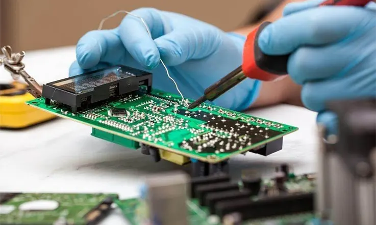
●Controlled Rework and Repair: In addition to initial assembly, processes for any necessary rework or repair also follow stringent guidelines, as defined by the IPC-7711/7721 standard. This ensures that even corrected assemblies meet the highest quality and reliability requirements.
Ultimately, the IPC standards provide the overarching framework that governs all the disciplines discussed in this series. From the material science of substrates and the physics of the solder joint, through the precise execution of process controls, to the final verification with reliability testing—all these activities are guided and validated by this common, objective language of quality.
Frequently Asked Questions (FAQ)
This section provides concise answers to common queries regarding the SMT soldering process and related technologies.
Q: What is the difference between a soak and a ramp-to-spike (RTS) thermal profile?
A: A soak profile uses a temperature plateau to equalize temperature on complex boards, minimizing thermal stress. An RTS profile is a faster, continuous ramp best for simple boards with uniform thermal mass.
Q: How is the voiding percentage in a solder joint measured and what is an acceptable limit?
A: Voiding is measured with an X-ray (AXI) system. Acceptable limits depend on the product class per standards like IPC-7095, but are often below 15-25% for high-reliability BGA solder balls.
Q: What is the difference between a “via-in-pad” and a “dog-bone” via connection?
A: A dog-bone connects a pad to an adjacent via with a short trace. A via-in-pad places the via directly in the pad for denser designs but must be filled and plated flat during fabrication to prevent soldering defects.
Q: Can different solder alloys be mixed in a single assembly process?
A: This is not recommended. Mixing alloys creates unpredictable, brittle intermetallics that compromise long-term reliability and make process control difficult.
Q: Does a “no-clean” flux truly require no cleaning after soldering?
A: Mostly, yes; the residues are designed to be benign. However, for certain high-reliability applications, cleaning may still be performed to ensure electrical performance or proper adhesion of conformal coatings.
Q: Why is a Design for Manufacturability (DFM) analysis recommended before fabrication?
A: A DFM analysis checks a PCB layout for features that could cause manufacturing or assembly defects. It proactively improves yield, reduces costs, and prevents problems by correcting the design before production begins.
A Partner in High-Reliability Manufacturing
Executing the complex processes of modern electronics assembly demands more than theoretical knowledge. It requires a synthesis of experience, advanced technology, and a systematic commitment to precision. This is a look into that methodology.
A Foundation of Quality
A robust Quality Management System (QMS) is the foundation of the entire operation, ensuring traceability, process stability, and continuous improvement.
●Adherence to IPC Standards: Operations are conducted in strict accordance with industry standards, with demonstrated capabilities to meet IPC-A-610 Class 2 and Class 3 requirements. This ensures your products are built to the level of reliability your application demands.
●Advanced Inspection and Data: Investment in state-of-the-art inspection technology, including 3D Automated Optical Inspection (AOI) and 3D Automated X-ray Inspection (AXI), allows not only for defect detection but also for the collection of process data. This data is used to keep all processes perfectly calibrated, preventing anomalies from occurring.
●Rigorous Process Control: From incoming material verification to final functional testing, every stage is governed by documented process controls, ensuring the final product precisely matches the design intent.
Value Through Efficiency and Transparency
Project success depends on effective budget management. Exceptional value is delivered through operational efficiency and financial transparency.
●Optimized Supply Chain: Established relationships with a global network of component suppliers allow for the sourcing of high-quality parts at competitive prices, minimizing procurement delays.
●Efficient Manufacturing: Investment in modern equipment and process optimization reduces manufacturing time and material waste, with these efficiency savings reflected in the final cost.
●Detailed and Clear Quotations: Quotations are comprehensive and transparent. A clear breakdown of costs is provided with no hidden fees, allowing for accurate and dependable project budgeting.
Predictability and On-Time Delivery
Meeting deadlines is a baseline requirement in the electronics market. The entire workflow is engineered for predictability and on-time delivery.
●Structured Project Management: Each project is assigned a dedicated manager who provides a clear schedule and regular status updates, ensuring clients are always informed.
●Flexible Timelines: A range of service options is available to match project needs, from rapid prototyping with expedited turnarounds to scheduled high-volume production.
●A Proven Record: A strong history of on-time delivery is a core performance metric, born from an understanding of the high cost of project delays.
Expert Engineering and Project Support
A successful partnership is built on clear communication and expert technical support.
●Engineering Consultation: Access to experienced engineers is available for complimentary Design for Manufacturability (DFM) and Design for Assembly (DFA) feedback. Identifying potential issues before production helps save time and resources on costly revisions.
●Single Point of Contact: Clients work with a dedicated representative who understands the project’s technical and commercial requirements, ensuring communication is always clear and effective.
●Responsive Communication: A commitment to responsiveness ensures technical queries and schedule updates receive prompt and helpful answers.
Advanced Manufacturing Capabilities
The facility and processes are equipped to handle the challenges of modern electronics design, from the straightforward to the highly complex.
●Advanced Component Handling: Proven processes are in place for assembling ultra-fine pitch components down to 01005, as well as complex packages including BGAs, CSPs, and QFNs.
●Technology Portfolio: Capabilities include advanced soldering techniques such as vacuum reflow for void reduction and selective soldering for mixed-technology boards.
●Material & Finish Flexibility: Support is provided for a vast range of PCB substrates, including FR-4, Rogers, Teflon, and Flex/Rigid-Flex materials, along with all major surface finishes like ENIG, ENEPIG, ImAg, and OSP.
Begin a Partnership Built on Expertise
The technical proficiency detailed throughout this guide is the basis of a reliable manufacturing partnership. To see how this expertise can be applied to your specific project, submit your design for a complimentary DFM analysis or request a detailed quotation today.