
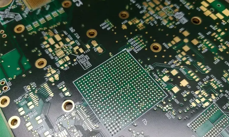
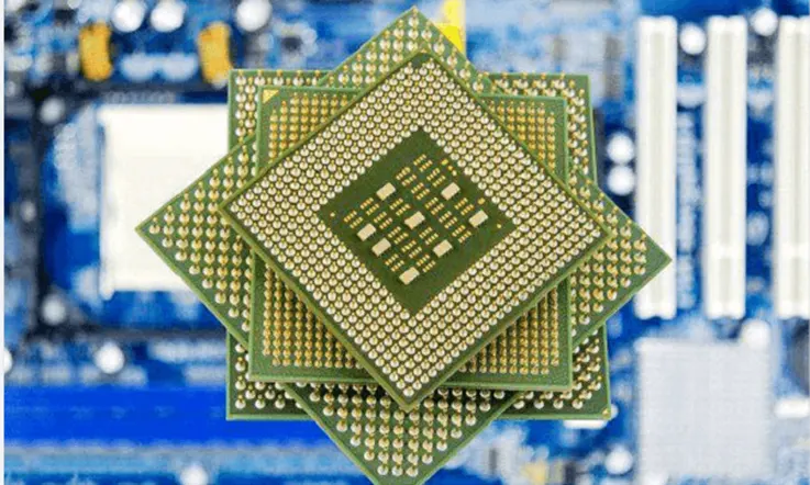
BGAs have become the industry standard for the packaging of a wide variety of modern multifunctional devices such as microprocessors and FPGAs as of today (Ball Grid Arrays).
A BGA package can be subdivided into micro BGAs and normal BGAs. Experienced PCB designers face new challenges when dealing with today’s electronics technology and the resulting demand for input/output availability.
In this article, we will discuss the application of BGA routing, the challenges of BGA routing, and some solutions for overcoming the challenges of BGA PCB design.
BGA Routing Guidelines
PCB designers are increasingly gravitating toward the use of ball grid arrays (BGAs) in response to the continuously growing demand in the market for smaller electronic devices that are able to perform a broader variety of functions. By utilizing BGAs, it is possible to use printed circuit boards (PCBs) that have a larger functionality in devices that are gradually smaller. BGAs are designed to be used on multilayer printed circuit boards (PCBs), on which vias are utilized to route signals between the layers.
Vias make the process of fabricating and assembling a PCB more complicated while adding flexibility to the process of designing a PCB. In the same way as tolerence considerations, placement limits, and best design principles are applicable to traces and components, they are also applicable to multilayer routing of BGA connections and the use of vias. You may make sure that your boards are less vulnerable to the common difficulties that can have an influence on the manufacturability and functionality of your product if you apply the best practices for BGA routing to them.
BGA Routing Guideline: What Is It?
The use of BGA routing presents a few challenges, all of which need to be taken into consideration during the design of the printed circuit board. Out of all of these, the one that has the most to do with assuring the dependability, manufacturability, and optimizing the signal integrity of the board is the one that is most significant.
Signal Integrity
Controlling the impedance, which has an effect on both transmission and reflection, is one of the most important aspects of maintaining signal integrity. The impedance can be regulated by ensuring that the trace widths of the forward and return lines are same, employing the suitable dielectric thickness, and putting in place a reference plane in the middle of the signal layers. It is also effective to install reference or ground planes between adjacent signal traces in order to reduce crosstalk. Since the signals are all on the same layer, it is extremely important to preserve the spacing between the traces.

Manufacturability
In order to optimize signal integrity, you need to take into consideration the manufacturability of the BGA routing scheme in addition to figuring out the number of layers that will be used (signal and reference). There are particular constraints and recommendations that are dependent on the manner in which the BGA connections are routed with one another and with the outside world. The capabilities of the manufacturer serve as a limiting factor for a number of aspects, including the number of layers, pitch angles, via sizes, type of hole drilling, and other considerations.
Reliability
The reliability of your board is determined by the quality of the board’s and how well your design synchronizes with the capabilities of the PCB manufacturer by employing good design for manufacturability (DFM) practices.
If you do not push the limitations or synchronize the limits very far, it is possible that you will end up with a PCB board that does not operate according to the design or at one point in time, may fail once it is deployed for use.
For example, problems with the material include the thickness of the solder mask, the structure of the copper grain, the thickness of the coverlay, and the weight of the copper. These problems lead to the failure of the board in the field.
In addition, the trace routing, which includes the selection of via, may also have an effect on the operation, which may then result in enormous expenses associated with replacement and recalls. By using the DFM check at JarnisTech, which integrates these concerns on any board, including Ball Grid Arrays, the design of the PCB layout will be aligned with the capabilities of the board maker.
If you apply DFM to boards that contain BGAs and incorporate these factors, your design will be aligned with the capabilities of your manufacturer. Let’s have a look at the many options that are available as well as the BGA routing rules for vias that, if used, will improve the signal integrity of your board as well as the PCB manufacturability of your board.
BGA Via Options
The first thing you need to do when building the routing system for your BGA is to figure out how many signal layers are necessary. This may be done by basing your decision on your signal integrity requirements. The following is a good rule of thumb: Number of Layers = Signals / (Routing Channels x Routing Per Channel). It is important to remember to provide reference planes wherever they are required. Using the quick-turn PCB design process, you can have your PCB layers up to 30 layers thick in a matter of days. This is a significant time savings. The following thing you need to do is figure out how to route the signals coming from your BGA. You have access to a variety of choices, but before you make a decision, it is important to think about the potential effects that each one could have on the PCB design you are developing:
Through Hole Via: Through hole routing, which extends across the entire board, is the most common approach for connecting through vias. Through-hole vias offer excellent signal integrity and are straightforward to construct, but they demand the most space.
Blind Vias: When routing directly from the Ball Grid Array, blind vias provide an alternative to through-hole. Blind vias allow for the use of staggered vias, stacked vias, or a combination of the two.
This enables a design that can have a higher component density when it comes to stacked vias. However, perfect alignment is not required for staggered vias, in contrast to stacked vias, which need to be aligned in a certain way. When it comes to the fabrication of the PCB, the tolerances ensure that the staggered vias may be implemented in a straightforward manner.
In the end, you will need to choose between the dogbone routing and the via-in-pad routing to determine which one is best for your needs. The following is a rundown of the space and complexity trade-offs that need to be considered.
Dogbone Routing: In this method of routing, the via is first disconnected from its pad, and then it is connected via a relatively short trace. This results in a form that resembles a dog bone in its general outline. In addition, dogbone routing does not need to be capped and filled as a technique that is necessary for the routing of vias in pads; as a result, the production of a pcb using dogbone routing is both more efficient and less complicated than manufacturing a via in pad.
In addition, there may be intricate designs, making it occasionally difficult to determine which via style is appropriate. So, this is an area in which the design team at JarnisTech can be of assistance. The decision that you make regarding the BGA routing will have a sizeable impact not only on the reliability of the signal but also on the turnaround time for the production of the circuit board.
When you put the rules for BGA routing into action, not only will you ensure that the PCB board can be manufactured, but you will also cut down significantly on the amount of time it takes to manufacture the printed circuit board.
Via-in-Pad Routing: With via-in-pad routing, the space requirements of through-hole vias can be decreased. The footprint is tiny and routing is simple for through-hole vias, but the design is complex. Blind vias, which enhance signal integrity, are challenging to route. Standard via-in-pad implementation adds considerable time to the PCB manufacture and assembly process. This can increase the manufacturing turnaround time by as much as thrice.

In order to make the most efficient use of available space, via-in-pad routing makes use of the smallest possible via and pad diameters. Because of the required level of precision, this could result in breakouts. The term “breakout” refers to the situation in which the via spreads beyond the pad. If the breakout happens in the direction of an incoming trace to the pad, this may be a severe issue that has to be addressed. In these circumstances, there is a risk of the signal’s integrity being compromised. Dogbone routing is a solution that can be used to avoid this.
Strategies to Deal with Problems in BGA PCB Design
Make sure that you begin the PCB Layout by utilizing a BGA. In most cases, a device’s primary processor will be a BGA. As a result, they might need to communicate with the many components that are already present on the board. The placement of the BGA’s largest component first, before using it to design your PCB layout, it is the practice that is most commonly followed.
But, this component does not have to be placed before anything else, nor does the location have to be locked when placed. The largest BGA, on the other hand, determines the fanout strategy and layer count that will be useful when routing the component.
Define Appropriate Exit Routes: BGAs with a higher layer count will require the planning of an exit route to involve routing traces through many rows of pins. Furthermore, some traces may contain high-speed signals, necessitating proper tracing spacing to avoid crosstalk.
Moreover, other signals might have a signals with slower configuration, allowing them to be brought closer together without producing an excessive amount of noise or increasing the likelihood of crosstalk.
Power and Ground: Using power rails is a very easy and straightforward method for controlling power connections into the BGA. This can be on either one or two plane layers. Putting power and ground on adjacent layers with a thin dielectric gap also contributes to maintaining power integrity by providing a capacitance that is high for the interplane.
Determine the PCB Layer Stack: Your PCB stackup’s layer count can be calculated using the BGA’s input/output count and pinout. As soon as the designer decides on the trace width, the lines with the controlled impedance must be routed into the BGA. In this way, you can calculate the layer thickness and the number of layers needed to keep the impedance constant.
Conclusion
The signal integrity and manufacturing viability of your PCB design will be significantly affected by the BGA routing you choose. However, keep in mind that your choice may probably lengthen the time it takes to make your board. The board’s manufacturability and the PCB’s build time can both be ensured by following BGA routing standards and using the optimal BGA routing scheme and techniques.
Additionally, JarnisTech is able to assist you in incorporating these best practices for BGA routing into the design of your PCB. As a provider of electronic manufacturing services as well as a maker of printed circuit boards (PCB) and assemblies, JarnisTech is in a unique position to know more than other suppliers regarding cost reduction, manufacturability, reliability, and turnaround time. Locate a PCB solutions provider that offers all-in-one services for your current or future projects involving PCB design, fabrication, and assembly. Do not hesitate to get in touch with us, as we will be able to offer you a significantly higher level of service for your upcoming PCB project.


