
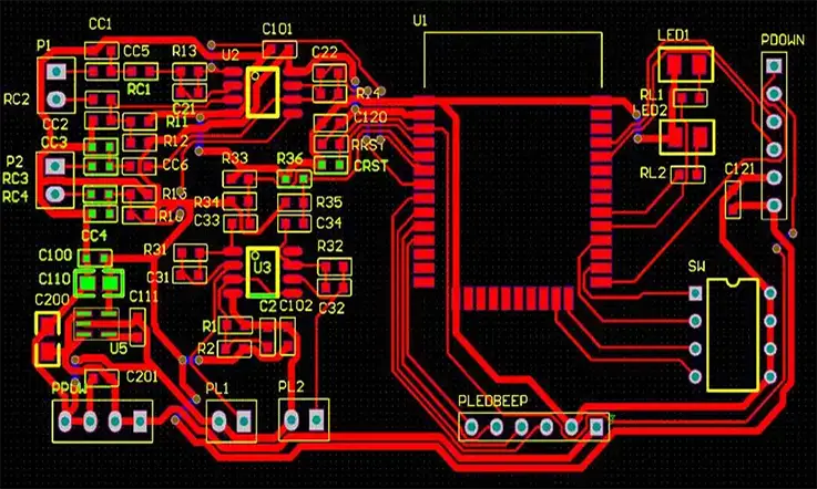
When it comes to designing printed circuit boards (PCBs), there’s a lot that goes into it. For anyone working in PCB manufacturing, assembly, or design, knowing the ins and outs of PCB design can make all the difference between a successful product and one that needs constant adjustments. From routing to layer stack-up, there are numerous tips that can elevate your design process.
But let’s be honest – when you’re deep into a project, every little decision can have a lasting impact. Whether you’re an experienced PCB Layout designer, a PCB engineer, or even someone just getting started, understanding key PCB design principles can save you time, money, and headaches.
So buckle up – we’re diving deep into PCB design tips that will not only improve your designs but help you get ahead of the industries.
Why PCB Design Tips Matter?
PCB design isn’t just about creating boards that function; it’s about understanding the bigger picture – the context in which these boards are going to be used. From the automotive sector to medical devices and consumer electronics, the expectations on PCBs have evolved significantly over the years. Today, the designs have to be more robust, versatile, and efficient than ever before. Understanding these nuances and applying the right PCB design tips can drastically reduce the chances of failure and save time in production.
In fields where precision and dependability aren’t just buzzwords but daily expectations, PCBs need to handle the challenges of their intended environments without flinching. Different industries impose unique demands, and tailoring your designs to meet these challenges is non-negotiable. Take high-performance electronics such as IoT devices, 5G equipment, or wearables—they require meticulous planning for high-speed signal routing, energy efficiency, and noise management to stay ahead of the curve. Meanwhile, sectors like automotive and medical technology add an extra layer of complexity, where your design choices directly influence not just functionality but also safety and reliability. In these cases, there’s no room for cutting corners, as the stakes are through the roof.
Let’s dive deeper into how the right PCB design tips can transform challenges into opportunities and help meet the rigorous demands across industries.
Transforming Design Challenges into Opportunities
For many designers, PCB design can initially seem like a straightforward series of tasks – placing components, routing signals, and making sure everything fits within the allotted space. However, real-world applications require much more than just meeting basic specifications. The demands in sectors like the automotive industry or medical technology often bring unforeseen challenges that require custom solutions.
Let’s break it down with a real-world example from the automotive industry. Consider the rugged conditions that a PCB in a vehicle has to endure – extreme temperatures, vibrations, and constant electromagnetic interference (EMI). This is not hypothetical; it’s something every designer has to face. PCBs in vehicles need to perform flawlessly under these harsh conditions, ensuring the safety of not only the electronics but also the lives of the people in the vehicle.
●Thermal management in PCB design takes center stage, particularly in automotive systems like electric vehicles (EVs), where high-current components generate significant heat. To keep things from going haywire, selecting materials with excellent thermal conductivity becomes a top priority. Equally important is arranging components with a keen eye for dispersing heat effectively, avoiding hotspots that could spell trouble. These design choices are not just about meeting technical specs; they ensure the board can handle the heat—literally and figuratively—in demanding environments where performance and reliability are non-negotiable.
●PCB design tips like EMI shielding and differential pair routing can also make a significant difference in automotive designs. Shielding sensitive components and ensuring the signal integrity of high-speed data lines helps prevent interference from other electronics within the vehicle, ultimately improving the performance and reliability of the overall system.
Below is an example of how temperature, vibration resistance, and EMI considerations are factored into different industries.
Comparison of Key PCB Design Factors for Different Industries:
| Design Factor | Automotive | Medical Devices | Consumer Electronics |
| Operating Temperature Range | -40°C to 125°C | 0°C to 60°C | 0°C to 85°C |
| Vibration Resistance | High (Shockproof PCB) | Low (Stable components) | Moderate (Resilient PCB) |
| EMI Resistance | High (EMI Shielding) | Moderate (Careful routing) | Low (Noise filtering) |
| Size Constraints | Moderate | Ultra-small (Miniaturization) | Small (Compact designs) |
| Signal Integrity | Critical (High-speed signal processing) | Very Critical (Reliability over years) | Moderate (Efficient routing) |
This table underscores the unique demands of PCB design across different industries and sheds light on how tailored strategies address specific challenges.. For instance, automotive PCBs need to withstand extreme temperatures and vibration, while medical device designs focus heavily on miniaturization and reliability, with extra care given to signal integrity for patient safety.
The Role of PCB Designers in Bridging Innovation and Practicality
As industries continue to innovate at a rapid pace, there’s always the need for PCB designers to bridge the gap between innovative technologies and practical solutions. Whether it’s working on 5G devices, IoT applications, or cutting-edge medical technology, the role of a PCB designer is to ensure these advancements can be translated into something that works reliably in the real world.
When designing PCBs for IoT devices, for instance, designers have to balance the need for compact designs with the performance of the circuit. These smart devices need to be small enough to fit into various consumer electronics while still maintaining strong signal integrity and low power consumption. But how do you make that happen?
●One approach is to use multi-layer PCBs which allow us to pack more functionality into smaller spaces. This reduces the size of the PCB without compromising its performance. In fact, some PCB design tips for IoT applications include focusing on fine-pitch components, rigorous layer stack-up strategies, and ensuring proper ground planes to minimize noise and interference. These strategies make IoT products more reliable, ensuring they work consistently even under changing conditions.
●On the other hand, the 5G revolution requires high-speed circuit design, and it’s up to us to figure out how to ensure these circuits can handle the massive data throughput while maintaining signal integrity. Whether it’s using microvia technology or controlled impedance traces, there are several advanced PCB design techniques that are shaping the future of 5G networks.
Here’s a breakdown of how certain PCB design principles and innovations impact these technologies, and how they’ve evolved over time.
PCB Design Considerations for IoT and 5G Technologies:
| Design Consideration | IoT Devices | 5G Technology |
| PCB Layer Count | 2-4 layers (Simple) | 6-12 layers (Complex) |
| Signal Integrity | Moderate (Low-frequency) | High (High-frequency) |
| Size | Ultra-compact (Miniaturized components) | Larger due to high-density components |
| Power Efficiency | High (Battery life is crucial) | Moderate (Data handling is key) |
| Advanced Routing Techniques | Low-frequency routing (Narrow traces) | High-frequency routing (Microvias, Controlled Impedance) |
This table highlights the stark differences in PCB design requirements across various technologies. For IoT devices, the focus leans heavily on achieving ultra-low power consumption, compact form factors, and sufficient signal performance to support wireless communication and energy efficiency. Meanwhile, 5G systems demand highly intricate multi-layer boards, precision-driven routing strategies, and exceptional signal performance to process high data rates without hiccups. These contrasting demands illustrate the tailored approaches needed for each technology, underscoring the importance of understanding the specific operational environment and performance expectations during the design phase.
Case Study: Success Stories in PCB Design
Let’s take a deeper look at how applying PCB design tips can lead to success stories in the real world. Consider the medical devices sector, where PCBs are required to meet stringent standards for reliability, performance, and miniaturization. Medical devices like pacemakers, hearing aids, or even diagnostic equipment rely on precise PCB designs for their functionality. These devices must not only be ultra-reliable but also compact enough to fit within the limited space of the device casing.
●A great example of success in PCB design can be seen in the medical field with pacemakers. Our designers have to ensure that the PCB can operate for years without fail, even in the human body. Applying thermal management techniques, signal integrity analysis, and precise placement of passive components helps in designing compact and reliable circuits for medical devices. The use of multi-layer boards helps in accommodating the necessary circuitry without increasing the overall size.
Design Strategies for Medical Device PCBs:
| Design Strategy | Pacemaker PCB | Medical Monitoring Device |
| Component Placement | Ultra-compact (Surface mount) | Compact but spacious for easy connections |
| Thermal Management | Use of heat sinks and vias for heat dissipation | Active cooling mechanisms or thermal pads |
| Signal Integrity | Ensuring minimal noise in small designs | Isolation and differential routing for accuracy |
| Reliability | High (Years of continuous use) | Moderate (Intermittent use) |
| Size Constraints | Extremely small (Fit in body) | Small but larger than pacemaker |
This table gives us a clear overview of the differences in PCB design considerations for two very different medical devices. While the pacemaker PCB needs to be ultra-reliable and compact, the medical monitoring device PCB must handle more complex tasks and may require additional space for connectors and cooling.
●Take consumer electronics as an example. Think about the sleek designs of smartwatches or wireless earbuds—these devices demand PCBs that are incredibly compact while delivering top-notch functionality. Designing for such tight quarters requires a laser-sharp focus on component placement, efficient power management, and clean signal routing to avoid interference. The trick is to strike a balance between innovation and practicality, ensuring performance doesn’t take a hit while keeping battery life in check. By leveraging smart techniques for miniaturization and rigorous reliability testing, we can craft PCBs that fit like a glove while packing a punch in performance.
From Concept to Reality: The PCB Design Process Unveiled
Starting a PCB design journey feels like stepping into a craft workshop where precision and creativity intertwine. From crafting the initial schematic to collaborating with production teams, each phase demands precision and ingenuity. A successful PCB design isn’t merely about functionality; it’s about building a reliable, efficient, and manufacturable product that stands the test of time. In this guide, we delve deep into the intricacies of turning your concept into a tangible, high-performance PCB.
Step-by-Step Walkthrough of a PCB Design Project
Designing a PCB involves navigating through a sequence of well-orchestrated stages, each serving as a stepping stone toward the final product. Here’s a closer look at the process:
1. Conceptualization and Schematic Design-
●Define Requirements: Outline the functional and operational needs of your PCB. This includes power requirements, communication interfaces, and mechanical constraints.
●Choose Components: Select components that meet performance specifications while balancing cost and availability.
●Create the Schematic: Use design software to map the logical connections between components.
2. PCB Layout and Routing-
●Placement Strategy: Group components based on their functional relationships and ensure accessibility for troubleshooting or modifications.
●Trace Routing: Optimize signal paths to minimize noise and maintain impedance. Tools like auto-routers can speed up this process but require manual review.
3. Validation and Fabrication Preparation-
●Design Rule Check (DRC): Validate that your layout adheres to the manufacturer’s specifications.
●Generate Gerber Files: Export files that detail copper layers, solder mask, and silkscreen for fabrication.
PCB Design Process Overview-
| Stage | Key Activities | Purpose |
| Conceptualization | Define specs, select components, design schematic. | Establish design foundation. |
| Layout & Routing | Component placement, trace optimization. | Ensure functionality and manufacturability. |
| Validation & Preparation | Run DRC, create fabrication files. | Ready the design for production. |
Troubleshooting and Iterating Your PCB Design
Once your initial design is ready, the real challenge begins—troubleshooting and refining. This phase ensures your PCB not only works but works well under all conditions.
1.Common Issues to Address-
●Signal Integrity Problems: Identify and rectify noise, crosstalk, or timing mismatches.
●Thermal Management: Pinpoint hotspots and assess heat dissipation strategies.
●Manufacturing Defects: Evaluate PCB prototypes for soldering issues or layer misalignments.
2.Iterative Refinement-
●Simulations: Use signal integrity and thermal analysis tools to predict and resolve potential issues.
●Rapid Prototyping: Employ technologies like 3D printing or quick-turn PCB services to test changes in real-world conditions.
●Feedback Loop: Collaborate with teams to incorporate findings into subsequent iterations seamlessly.
Collaboration Between Design, Manufacturing, and Assembly Teams
A seamless PCB design process hinges on effective communication across all teams involved. Designers, manufacturers, and assemblers must work as a unified entity to avoid delays and minimize errors.
1.Early-Stage Coordination-
●DFM Insights: Engage manufacturers early for input on layout adjustments that simplify fabrication.
●Component Libraries: Standardize component choices to streamline procurement and assembly.
2.Production-Phase Synchronization-
●Clear Documentation: Provide comprehensive files, including BOMs (Bills of Materials), assembly drawings, and test plans.
●Proactive Issue Resolution: Use shared platforms for real-time updates on production challenges.
Collaboration Best Practices-
| Team | Role | Action for Effective Collaboration |
| Design Team | Create schematics and layouts. | Ensure files are DFM-ready. |
| Manufacturing Team | Fabricate boards. | Provide DFM feedback early. |
| Assembly Team | Assemble components onto PCBs. | Highlight placement or orientation concerns. |
PCB Design Tips for Achieving Excellence in Layout and Routing
When designing a PCB, the layout and routing are at the heart of how well your board will perform, and every decision made plays a part in shaping that success. From signal quality to power distribution and heat management, we must carefully balance all these factors to ensure the board functions as intended. Paying attention to these details can make or break the performance of your product, so staying on top of the design process is a must to achieve reliability and efficiency.
In this section, we’ll explore a few PCB design tips that can guide you to success in your layout and routing efforts. From signal integrity to power integrity, and even techniques for designing high-density interconnects (HDI), we’ll cover the essentials you need to create a reliable PCB that’s ready for high-performance applications.
Mastering PCB Layout Rules for Signal Integrity
When it comes to signal integrity, every move you make during PCB layout can either boost or hinder your circuit’s performance. Issues like noise, cross-talk, and signal reflections are no small potatoes—they can cause serious disruptions, whether you’re dealing with basic communication circuits or tackling more advanced systems, like those found in 5G technology. Getting these factors right is the difference between smooth sailing and constant headaches, especially when it comes to high-speed data transfer. So, keep your layout tight, and don’t let these problems sneak up on you!
1.Best Practices for Signal Integrity-
Here’s where proper layout can make a big difference. Proper component placement is a fundamental aspect of signal integrity. By placing high-speed components as close to each other as possible and routing the traces for minimal distance, you can drastically reduce the potential for interference and signal loss. For instance:
●Minimize trace lengths: The shorter the trace, the less likely it is to act as an antenna that attracts electromagnetic interference (EMI).
●Use of ground planes: Having a dedicated ground plane provides a clear reference for signals and can help reduce noise.
2.Common Signal Integrity Issues and Fixes-
| Signal Integrity Issue | Description | Design Tip |
| Cross-talk | Interference between adjacent signal traces | Keep high-speed traces far apart; use shielding |
| Reflection | Signal bouncing due to impedance mismatch | Ensure impedance matching along the signal path |
| EMI | Interference caused by electromagnetic waves | Implement proper shielding and grounding |
Example: High-Speed Data Transfer in 5G Systems
When designing a PCB for a 5G network device, maintaining strong signal integrity is a must. High-frequency signals in 5G systems can easily degrade if not properly managed. By sticking to best practices, such as routing differential pairs and ensuring controlled impedance for traces, you’ll set your design up for success. These strategies help keep high-speed data flowing smoothly and prevent interference, ensuring your 5G device can meet performance expectations without a hitch. Getting this right is how you avoid signal issues and make sure your device delivers the goods.
H3: Effective Routing Techniques to Ensure Power Integrity
Power integrity ensures that a PCB functions reliably. Without a stable power delivery system, even the best components will underperform. In PCB design, making sure the board receives consistent power is a must. This directly impacts the performance and longevity of your components. When power delivery is off, voltage drops and noise can cause unpredictable behavior or even component failure. Planning an effective power strategy from the beginning is the way to keep everything working like it should. A well-thought-out design keeps things in check, letting the board function as intended.
1.Routing for Power Integrity-
For optimal power integrity, focus on impedance matching and keeping power paths short. Reducing the length of power traces minimizes voltage drops and IR losses, ensuring better system performance. Also, reducing the overlap between power and signal traces helps limit crosstalk, which can interfere with your circuit. With these adjustments, your PCB will perform with fewer issues and greater reliability, giving your design the stability it needs to perform as intended.
2.Balancing Ground Planes-
A balanced ground plane is the foundation for solid power integrity. If it’s not up to par, you could end up with ground bounce—resulting in signal interference and other issues that’ll mess with your system’s performance. To avoid these headaches, your ground plane needs to be optimized to efficiently handle return currents. The goal is to keep it as continuous and seamless as possible. When it’s done right, the ground plane ensures smooth and stable performance, helping your PCB avoid noise, distortion, and unwanted voltage shifts. Proper ground design is a must to keep everything running without a hitch.
3.Key Considerations for Power Integrity-
| Power Integrity Factor | Consideration | Design Tip |
| Voltage Drop | The decrease in voltage as it travels through traces | Use wider traces and thicker copper for power paths |
| Ground Plane Quality | The quality and continuity of the ground return path | Ensure solid grounding and low impedance paths |
| Current Carrying Capacity | The trace width needed to carry sufficient current | Calculate trace width based on current load |
Example: Power Integrity in Consumer Electronics
Consider a PCB design for a smartphone. The power rails in such devices must supply a stable voltage to various components such as processors, screens, and sensors. By routing the power lines efficiently and providing a solid ground return path, you ensure that each component gets the necessary current without voltage dips. This ensures the smartphone operates reliably, with no issues like random reboots or lag due to unstable power.
Advanced Techniques for High-Density PCB Layout
With modern technology demanding increasingly compact designs, creating high-density interconnect (HDI) PCBs has become a necessity. HDI designs allow for greater functionality in a smaller footprint, making them ideal for smartphones, wearable devices, and other miniaturized electronics.
1.Designing HDI PCBs-
To achieve success in high-density PCB layout, you need to ensure that miniaturization doesn’t sacrifice signal integrity or thermal performance. Here are some practical tips:
●Use microvias: Microvias enable you to create more compact designs by stacking them within the PCB layers, allowing for high-density connections without increasing the overall board size.
●Stacked and Blind Vias: Stacked vias allow multiple layers of connections, minimizing the required PCB real estate for routing. Blind vias provide internal connections between specific layers without going through to the outer layers.
2.Balancing Miniaturization with Thermal Performance-
One of the challenges with high-density PCBs is maintaining thermal performance. With more components packed into smaller spaces, heat dissipation becomes a concern. Here’s how you can balance miniaturization with thermal management:
●Use thermal vias to channel heat away from sensitive components.
●Spread-out power components across the board to avoid hotspots.
Optimize component placement to allow for proper airflow, which is often overlooked in miniaturized designs.
3.High-Density PCB Design Considerations-
| Design Aspect | Consideration | Design Tip |
| Miniaturization | Making the PCB smaller while retaining performance | Use microvias and fine-pitch components |
| Thermal Management | Preventing heat buildup in high-density designs | Implement thermal vias, heat sinks, and spread-out power components |
| Signal Integrity | Ensuring clear signal transmission in densely packed areas | Use shielding, controlled impedance, and careful trace routing |
PCB Design Tips for Thermal Management and Power Distribution
Thermal management and power distribution are two fundamental elements in PCB design, especially in high-power applications. Without proper heat dissipation or efficient power delivery, you risk facing performance issues and potential component failure. Whether your project involves consumer electronics, automotive systems, or industrial equipment, getting these areas right is necessary for the PCB to function effectively and endure over time. In this section, we’ll explore practical approaches to managing heat, optimizing power distribution, and ensuring your design maintains stability and reliability under demanding conditions. With the right strategies, your design will perform with confidence, even in challenging environments.
Effective Heat Management in High-Power PCBs
Managing heat is one of the toughest challenges in high-power PCB design. As components draw more current, they generate more heat, and improper heat dissipation can cause thermal stress, leading to component degradation or even circuit failure. Designing for heat management requires a careful balance of material selection, layout, and thermal design techniques.
1.Understanding the Importance of Thermal Management-
In high-power designs, managing heat is a big deal when it comes to ensuring long-term performance and durability. Components like power transistors, LED drivers, and processors can quickly become heat hotspots if the design doesn’t account for heat dissipation. Too much heat can cause components to fail early, or even trigger thermal runaway, leading to serious system breakdowns. That’s why thermal management isn’t something you want to leave to chance—it needs to be baked into the design process from the start. By addressing heat challenges up front, you’ll avoid potential problems down the line, keeping everything in check and working as it should.
2.Best Practices for Heat Dissipation-
●Heat Sinks: Add heat sinks to power-hungry components. These help increase the surface area available for heat dissipation and keep the temperature within an acceptable range. Ensure they are positioned correctly on the PCB to maximize airflow.
●Thermal Pads and Compounds: Use thermal pads or thermal interface materials (TIMs) between hot components and the PCB or heat sink to improve thermal transfer efficiency.
●Component Placement: Place high-power components away from sensitive signal areas. This reduces the risk of thermal coupling that could negatively impact signal integrity.
3.Heat Management Techniques-
| Technique | Description | Design Tip |
| Heat Sink | Attach to power components to dissipate heat. | Ensure correct size and placement for effective heat transfer. |
| Thermal Vias | Drill vias to channel heat to layers with better thermal properties. | Use multiple vias around heat-sensitive components. |
| Component Spacing | Ensure components generating heat are spaced correctly. | Avoid clustering power components in one area. |
Power Distribution and Grounding Best Practices
Power distribution involves making sure that each component on the PCB gets the power it needs, while avoiding voltage drops, noise, or crosstalk. A strong grounding approach is just as important to prevent issues like ground loops, voltage shifts, and electromagnetic interference (EMI). Without a solid grounding and power strategy, the stability and reliability of your system could be compromised, leading to performance problems. Getting these elements right from the start helps keep your design clean and avoids future headaches.
1.Optimizing Power Distribution Networks (PDN)-
An effective power distribution network (PDN) ensures that each component receives the required voltage and current without significant voltage fluctuations. Here are some tips for optimizing the PDN:
●Use Decoupling Capacitors: Position decoupling capacitors as close as possible to the power pins of your high-speed ICs to reduce power noise and smooth out voltage variations. This helps ensure stable operation of sensitive components.
●Design for Low-Voltage Drops: Design wide power traces to minimize voltage drop across the PCB. Use multiple layers in the PCB to distribute power effectively and reduce resistance.
2.Effective Grounding Techniques-
A poor grounding design can introduce significant noise and voltage instability into your PCB. The following best practices can help ensure proper grounding:
●Solid Ground Plane: Always use a solid ground plane for minimal impedance and to prevent unwanted signal interference. This also helps reduce EMI and ensures more reliable signal transmission.
●Single-Point Grounding: For analog or sensitive circuits, use single-point grounding where all the grounds converge at a single point to prevent ground loops that can distort signals.
3.Power Distribution and Grounding Considerations-
| Design Factor | Consideration | Design Tip |
| Decoupling Capacitors | Reduce noise and stabilize power supply. | Use a range of values and place them close to power pins. |
| Power Trace Width | Reduce voltage drop across power traces. | Calculate using the IPC-2221 standard for trace width. |
| Ground Plane Quality | Minimize noise and voltage fluctuations. | Keep ground plane as continuous and uninterrupted as possible. |
Using Thermal Vias and Heat Sinks for Optimal Heat Dissipation
Thermal vias and heat sinks are must-haves when it comes to keeping your PCB within safe temperature limits. These components work hand-in-hand to move heat away from the critical areas of your design, especially in multi-layer PCBs where heat tends to build up in those inner layers. Without them, you risk overheating, which could damage your components or reduce the lifespan of your board. By integrating these heat management solutions early on, you’re setting your PCB up for long-term reliability, making sure it doesn’t run too hot under pressure.
1.Integrating Thermal Vias-
Thermal vias allow heat to be transferred from hot components to lower layers where it can be dissipated more effectively. Here’s how to incorporate them into your design:
●Multiple Thermal Vias: Use multiple small vias around high-power components like power transistors or LED drivers to distribute heat across the PCB layers.
●Via Size and Placement: The size and placement of thermal vias can significantly impact heat dissipation. Ensure they are placed as close as possible to the component and aligned with thermal planes in the internal layers of the PCB.
2.Adding Heat Sinks to the Design-
Heat sinks are passive cooling solutions that increase the surface area for heat dissipation. They can be attached to the PCB using screws or adhesives. Here’s how to integrate them:
●Size and Material: Choose heat sinks that are appropriately sized for your design, considering both thermal load and available space. The material should ideally be aluminum, which provides good thermal conductivity.
●Placement: Heat sinks should be positioned above high-power components or power regulators to effectively draw heat away from these areas.
3.Thermal Management Tips for Heat Dissipation-
| Thermal Management Technique | Consideration | Design Tip |
| Thermal Vias | Allow heat transfer from surface components to inner layers. | Use multiple vias for effective heat distribution. |
| Heat Sinks | Enhance heat dissipation by increasing surface area. | Select aluminum material and ensure proper fit. |
| Via Size and Placement | Optimize via size and placement for heat transfer. | Place vias close to heat-sensitive components. |
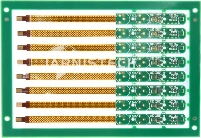
PCB Design Tips for Manufacturability and Assembly
Designing a PCB isn’t just about ensuring functionality or performance—it’s also about making it manufacturable and assembly-friendly. Poor design choices can lead to higher production costs, longer lead times, or, worse, outright failures during manufacturing. By incorporating Design for Manufacturability (DFM) principles and optimizing for assembly from the outset, you can bridge the gap between concept and production, ensuring a smooth transition into mass manufacturing. Below, we’ll explore DFM techniques, prototyping strategies, and assembly optimizations that will help you avoid costly errors and boost production yields.
DFM (Design for Manufacturability) Tips
Achieving a design that is easy to manufacture requires attention to layout, materials, and process compatibility. Implementing effective DFM strategies ensures that your PCB can be produced with minimal challenges, reducing costs and improving efficiency.
1.Layout Guidelines for Manufacturability-
When laying out a PCB, ensure the design adheres to industry-standard tolerances and is compatible with automated manufacturing processes. Consider the following:
●Component Placement and Clearance: Proper spacing between components prevents assembly issues like solder bridging and ensures that automated machines can easily handle the board.
●Trace and Via Design: Maintain minimum trace widths and via sizes as per your manufacturer’s capabilities. Use teardrop vias to improve robustness during manufacturing.
●Panelization: Design your PCB with panelization in mind to allow multiple boards to be processed simultaneously, optimizing production throughput.
2.Material Compatibility-
Select PCB materials that align with your manufacturer’s processes. Ensure compatibility with soldering techniques, thermal expansion requirements, and specific surface finishes (e.g., ENIG, HASL) used during assembly.
3.DFM Checklist for PCB Design-
| Design Aspect | Requirement | Tips for Success |
| Component Clearance | Maintain minimum spacing as per IPC standards. | Consult your manufacturer’s DFM guidelines. |
| Trace Width and Spacing | Ensure dimensions meet manufacturing tolerances. | Use design rule checks (DRC) in CAD software. |
| Panelization | Optimize for board size and manufacturing efficiency. | Use v-scoring or mouse bites for separation. |
Prototyping and Testing for High-Yield PCB Production
Before committing to large-scale production, prototyping and testing are indispensable steps to identify design flaws and refine the manufacturing process. Skipping these steps often results in low yields and costly rework.
1.Prototyping Best Practices-
●Functional Prototypes: Start with a functional prototype to test the core electrical and mechanical aspects of your design.
●Test Manufacturing Feasibility: Create a small batch with your intended manufacturing partner to validate the design’s production readiness.
2.Testing Techniques for Error Detection-
To catch potential issues early, implement the following:
●AOI (Automated Optical Inspection): Use AOI to detect soldering and component-placement errors.
●In-Circuit Testing (ICT): Verify electrical functionality and connectivity by probing key points on the PCB.
●Thermal Imaging: Use thermal cameras to identify hotspots that could lead to failures during operation.
3.Prototyping and Testing Workflow-
| Phase | Objective | Common Tools/Methods |
| Prototyping | Validate design and manufacturability. | CAD software, small batch runs. |
| Electrical Testing | Check signal integrity and power delivery. | Oscilloscopes, TDR (Time-Domain Reflectometers). |
| Manufacturing Testing | Ensure assembly precision and production yield. | AOI, ICT, X-ray inspection. |
Optimizing PCB Assembly for Efficiency and Accuracy
Efficient PCB assembly depends on designs that are built for smooth automation. Features like fiducials, optimized pick-and-place paths, and uniform component orientations are all about streamlining the process, boosting yield, and cutting down on production time. When every part is in the right place and everything is laid out for easy handling, it’s like a well-oiled machine, ensuring quick turnaround without sacrificing quality. By getting the design details just right, you’ll make the whole assembly process a breeze, reducing costly errors and delays along the way.
1.Pick-and-Place Optimization-
Modern assembly lines depend on pick-and-place machines to position components. To optimize this process:
●Consistent Component Orientation: Align components in the same direction wherever possible to speed up machine programming and reduce placement errors.
●Minimized Component Variants: Reduce the number of unique component types to simplify inventory and assembly.
2.Fiducials and Solder Mask Considerations-
●Fiducials: Add global and local fiducials to your PCB to help assembly machines align and place components accurately.
●Solder Mask Design: Ensure solder mask openings are well-defined to prevent solder bridging and other assembly defects.
3.Assembly Optimization Tips-
| Optimization Area | Best Practice | Benefit |
| Component Orientation | Align components in the same direction. | Reduces machine setup time and errors. |
| Fiducial Placement | Add at least three global fiducials. | Enhances placement accuracy during assembly. |
| Solder Mask Design | Maintain clean openings for component pads. | Prevents solder-related defects. |
PCB Design Tips for Specialized Applications and Industries
Specialized applications demand tailored PCB design approaches to meet stringent industry requirements. Whether dealing with extreme environmental conditions, optimizing for renewable energy solutions, or shrinking consumer electronics, each sector comes with unique challenges that push the boundaries of conventional design practices. By mastering specific techniques for industrial, solar, and consumer applications, you can unlock the full potential of your designs while ensuring reliability, efficiency, and scalability. Let’s dive into the nuances of PCB design for specialized industries and explore how to achieve excellence.
Industrial PCB Design Tips for Harsh Environments
Designing PCBs for industrial environments comes with its challenges. With factors like extreme temperatures, moisture, dust, and electromagnetic interference (EMI) at play, you need a design that can handle the heat—literally and figuratively. The key here is ensuring your board remains solid and dependable under tough conditions. That means using durable materials, opting for protective coatings, and planning for thermal management. It’s all about staying ahead of potential issues and designing for the long haul. From component placement to EMI shielding, every detail needs to be on point to keep things running smoothly, no matter how demanding the environment.
Environmental Considerations-
1.Temperature Tolerance: Use materials like FR-4 TG130+ or ceramic substrates for high-temperature stability.
2.Moisture Protection: Implement conformal coatings to protect the board from humidity and corrosive agents.
3.Vibration Resistance: Reinforce solder joints and use shock-absorbing mountings for vibration-prone environments.
EMI/EMC Compliance-
●Shielding: Use ground planes and shielding enclosures to minimize EMI susceptibility.
●Filtering: Include ferrite beads and capacitors to suppress noise at critical nodes.
●Trace Layout: Route high-frequency signals away from sensitive components.
Industrial PCB Design Checklist-
| Design Aspect | Best Practice | Benefit |
| Material Selection | High-temperature and durable substrates. | Enhances lifespan in extreme environments. |
| Coating | Conformal coatings for moisture and dust. | Protects against environmental damage. |
| EMI Mitigation | Ground planes and effective filtering techniques. | Reduces interference for reliable operation. |
Designing PCBs for Solar Power Systems
Solar power systems require PCBs optimized for energy efficiency, thermal performance, and cost-effectiveness. These designs must operate seamlessly under varying conditions while maximizing energy conversion.
Energy Efficiency-
1.Power Conversion: Use low-resistance copper traces to reduce energy losses in high-current paths.
2.Component Selection: Choose for high-efficiency MOSFETs and diodes to enhance power conversion.
Thermal Management-
●Heat Dissipation: Incorporate thermal vias and heat sinks for components like power transistors and voltage regulators.
●Thermal Simulation: Use tools to simulate heat distribution across the board to identify hotspots.
Key Design Tips for Solar PCBs-
| Factor | Design Approach | Impact |
| Energy Efficiency | Low-resistance traces and efficient components. | Reduces power loss and increases reliability. |
| Thermal Dissipation | Thermal vias, heat sinks, and simulations. | Improves performance under high load. |
| Scalability | Modular design to support varying panel sizes. | Simplifies deployment in diverse setups. |
Consumer Electronics PCB Design: Minimizing Size Without Compromising Performance
In the fiercely competitive consumer electronics market, miniaturization is king. Yet, achieving smaller footprints without sacrificing performance or reliability is a delicate balancing act.
Miniaturization Techniques-
1.HDI Technology: Use microvias and blind/buried vias to pack more functionality into smaller PCBs.
2.Component Placement: Arrange components for optimal routing efficiency and minimal interference.
3.Flexible PCBs: Leverage flex and rigid-flex PCBs for unconventional form factors like wearables and foldable devices.
Reliability and Cost-Effectiveness-
●Thermal Design: Even compact designs need effective heat dissipation. Use copper pours and thermal pads.
●DFM (Design for Manufacturability): Simplify assembly by aligning components consistently and ensuring trace accessibility.
Key Metrics for Consumer Electronics PCBs-
| Metric | Design Strategy | Result |
| Board Size | Use HDI and flexible PCB technology. | Maximizes functionality in limited space. |
| Thermal Performance | Copper pours and thermal vias. | Maintains stability in compact designs. |
| Cost Control | Streamlined assembly processes. | Keeps production affordable. |
How to Avoid Five Common Mistakes When Designing PCBs?
Designing a PCB is like orchestrating a symphony—each element must harmonize perfectly to achieve optimal performance. Yet, even seasoned designers can stumble upon common pitfalls that derail their projects. By understanding and addressing these challenges early, you can save time, reduce costs, and elevate the efficiency of your design-to-production process. Here, we explore five frequent mistakes in PCB design and how to dodge them with precision.
Missing the Board Outline
1.Why It Matters-
The board outline isn’t just a visual guide—it defines the physical constraints and shape of your PCB. Without this, your entire design risks misalignment during manufacturing, leading to waste or rework.
2.How to Avoid It-
●Define Early: Establish the board outline at the start of your design process.
●Use CAD Tools: Most PCB design software allows you to define outlines with precise dimensions.
●Optimize for Fit and Functionality: Adjust the shape based on the enclosure or application requirements, ensuring all components fit snugly.
3.Pro Tip-
Experiment with different shapes if aesthetics or unconventional form factors are a priority, but always validate manufacturability.
Incorrect Landing Patterns
1.Why It Matters-
Landing patterns, or footprints, are the blueprint for placing components. Errors here can result in soldering difficulties, connectivity issues, or even a failed PCB.
2.How to Avoid It-
●Manual Verification: Double-check pad-to-pad spacing and component alignment.
●Reference Standards: Use IPC-compliant footprints when available.
●Test Layouts: Simulate assembly processes to identify and resolve conflicts.
Landing Pattern Best Practices-
| Checklist Item | Reason | Tips |
| Verify Pad Spacing | Prevent short circuits or soldering issues. | Use measurement tools in your software. |
| Ensure Component Fit | Avoid mechanical interference. | Cross-reference datasheets. |
| Include Test Points | Facilitate debugging and testing. | Place accessible test pads. |
Overextending High-Speed Traces
1.Why It Matters-
●High-speed traces carry signals where timing and integrity are paramount. Excessive length or improper routing can lead to noise, reflections, and signal degradation.
2.How to Avoid It-
●Keep It Short and Straight: Avoid unnecessary bends and loops.
●Match Impedance: Use controlled-impedance routing techniques.
●Layer Management: Place high-speed signals on dedicated layers with minimal crossovers.
3.Pro Tip-
●Simulate signal behavior using tools like HyperLynx to visualize potential issues before fabrication.
Using Blind or Buried Vias Carelessly
1.Why It Matters-
While blind and buried vias save space, they complicate manufacturing and prototyping. Their misuse can lead to connectivity problems or increased costs.
2.How to Avoid It-
●Stick to Through-Hole Vias: For simpler designs, stick to traditional vias unless absolutely necessary.
●Collaborate with Manufacturers: Discuss via requirements early to ensure compatibility with their capabilities.
●Design for Testing: Ensure all vias are accessible for troubleshooting during the prototype phase.
Poor Placement of Decoupling Capacitors
1.Why It Matters-
Decoupling capacitors stabilize voltage supply and filter noise. Incorrect placement can compromise the stability and functionality of your PCB.
2.How to Avoid It-
●Close Placement: Position decoupling capacitors as close as possible to the power pins they serve.
●Use Proper Values: Pair capacitors of different values to cover a broader frequency range.
●Consider Low-Pass Filters: Combine capacitors with inductors to create effective noise suppression circuits.
3.Pro Tip-
●Plan capacitor placement during the schematic phase to avoid last-minute shuffling in the layout stage.
PCB Design Tips for Emerging Technologies and Future Trends
As technology evolves at breakneck speed, the demands on PCB design grow more intricate and specialized. Emerging technologies like 5G, IoT, and AI have transformed how PCBs are conceptualized, pushing boundaries in signal integrity, routing optimization, and eco-friendly practices. Circuit Boards Designers are now navigating uncharted territories, requiring adaptive strategies to ensure their designs stay ahead of the curve. Below, we unpack actionable insights for tackling the challenges posed by cutting-edge applications and future trends.
5G and IoT PCB Design Challenges
The rise of 5G and IoT has redefined the communication landscape, introducing significant challenges for PCB designers. These technologies demand ultra-fast signal transmission, efficient power distribution, and minimal interference across complex networks.
Signal Integrity and High-Speed Routing-
1.Controlled Impedance: High-frequency signals in 5G PCBs necessitate controlled impedance routing to prevent signal degradation. Employ differential pairs and precise trace spacing.
2.Material Selection: Use low-loss materials like Rogers laminates to reduce signal attenuation at higher frequencies.
3.Crosstalk Mitigation: Isolate high-speed traces and utilize ground planes to shield signals.
Power Distribution Optimization-
●Decoupling Capacitors: Place capacitors close to ICs to maintain stable power delivery.
●Power Plane Layout: Design wide, low-resistance power planes to minimize voltage drops.
Key Considerations for 5G and IoT PCBs-
| Challenge | Design Strategy | Outcome |
| Signal Integrity | Controlled impedance, low-loss materials. | Reliable high-speed communication. |
| Crosstalk Reduction | Ground planes, proper trace isolation. | Cleaner signal transmission. |
| Power Stability | Decoupling capacitors, wide power planes. | Enhanced device reliability. |
Leveraging AI and Simulation Tools for PCB Design
Modern PCB design is revolutionized with the use of AI tools and simulation software, making complex tasks easier and ensuring design precision. These innovations streamline the PCB layout and routing process, helping designers create efficient, error-free boards with less effort. Thanks to AI, designers can quickly pinpoint potential issues and optimize their designs, leading to faster, more accurate results. With simulation software, the whole process becomes smoother, enabling thorough testing before moving to production. It’s a new age for PCB design where technology takes the wheel, allowing for higher-quality boards with less hassle.
AI-Driven Automation-
1.Layout Optimization: AI algorithms can suggest optimal placement for components, reducing electromagnetic interference and ensuring better performance.
2.Routing Assistance: Automate tedious routing tasks, saving hours of manual work while maintaining precision.
Simulation Software Benefits-
●Thermal Analysis: Simulate heat distribution to identify hotspots and adjust the layout for improved cooling.
●Signal Integrity Verification: Validate high-speed traces and detect potential issues before fabrication.
Advantages of AI and Simulation in PCB Design-
| Feature | Application | Benefit |
| AI Automation | Layout and routing optimization. | Reduced design time and higher accuracy. |
| Thermal Simulation | Heat dissipation planning. | Ensures longevity and reliability. |
| Signal Integrity Tools | High-frequency circuit validation. | Prevents costly post-production errors. |
Sustainable PCB Design for Eco-Friendly Manufacturing
As sustainability becomes a top priority, many PCB designers are embracing eco-friendly materials and practices to reduce environmental impact without compromising performance.
Eco-Friendly Materials-
1.Lead-Free Solder: Transition to RoHS-compliant materials to eliminate harmful lead usage.
2.Biodegradable Substrates: Explore options like biodegradable laminates for reduced waste.
Design for Recycling-
●Modular Design: Create boards that can be easily disassembled for component recovery.
●Labeling Standards: Clearly mark components for easier recycling and disposal.
Balancing Sustainability with Cost-
Eco-friendly designs often face the challenge of balancing cost-effectiveness. By integrating sustainable materials strategically and optimizing the manufacturing process, our designers can achieve both performance and environmental responsibility.
Sustainable PCB Design Practices-
| Aspect | Sustainable Approach | Benefit |
| Materials | Lead-free solder, biodegradable substrates. | Reduced environmental footprint. |
| Recyclability | Modular, labeled designs. | Simplified end-of-life disposal. |
| Cost vs. Sustainability | Process optimization for material use. | Economic feasibility with eco-friendly focus. |
Why Partner with JarnisTech for Your PCB Design Needs?
At JarnisTech, we’re all about precision, flexibility, and know-how when it comes to PCB design and layout. Whether you’re starting fresh with a schematic or reverse-engineering an existing design, we’ve got the skills and tools to make your project come to life. From double-sided to multi-layer PCBs, we handle it all – from medical to military applications, and everything in between. JarnisTech is your trusted partner for high-quality, high-performance PCB solutions, designed to meet your specific needs and ensure a smooth production process from start to finish. No matter the complexity, we’ve got your back!
1.Comprehensive PCB Design and Reverse Engineering Services
We offer a full spectrum of PCB design and layout services to meet the most demanding specifications. Our offerings include:
●Custom PCB Design: Supporting double-sided and multi-layer designs, radial layouts, and non-standard geometries.
●Reverse Engineering: Extracting PCB designs and generating complete Gerber data from physical samples.
Our designs cater to a variety of technologies:
●Digital, analog, RF, and power systems.
●High-speed and high-density applications.
●Flexible circuits and high-power PCBs.
Our advanced design tools ensure precision, while our deliverables include everything from drill and Gerber files to custom-formatted assembly and fabrication documents.
| Capability | Details |
| Double-Sided & Multi-layer | Robust designs for complex applications. |
| High-Speed/High-Density | Perfect for compact and performance-heavy devices. |
| Custom Geometries | Radial and non-standard shapes supported. |
2.Tailored Deliverables for Seamless Manufacturing
We understand that every project has unique requirements. That’s why we deliver files in formats tailored to your specifications.
●Manufacturing and Assembly Files: Ensuring smooth production.
●Custom Drawings: In your preferred format for easy interpretation.
Our streamlined process ensures minimal back-and-forth, saving you time and effort.
3.Specialized PCB Design Across Industries
JarnisTech designs PCBs for a diverse range of applications, ensuring top-tier performance no matter the field:
●Medical: High-reliability PCBs for sensitive healthcare devices.
●Military: Rugged designs for mission-critical applications.
●Automotive: Durable PCBs for automotive electronics.
●Industrial: Boards optimized for harsh environments.
●Aerospace: Lightweight yet robust designs for aviation and space tech.
Other applications include communications, lighting, and computing.
| Industry | Specialization |
| Medical | Precision and stability for life-saving devices. |
| Aerospace | Lightweight designs with high thermal resistance. |
| Industrial | Durability under extreme conditions. |
4.Why Choose JarnisTech?
With a proven track record and industry-leading expertise, JarnisTech delivers more than just PCBs—we deliver solutions. Here’s why you should work with us:
●Expertise: Our team has extensive experience across a range of technologies and applications.
●Customization: We adapt to your needs, offering tailored designs and deliverables.
●Collaboration: Open communication ensures your vision is realized with precision.
●Reliability: On-time delivery and adherence to quality standards.
Let’s Bring Your PCB Project to Life
Ready to kickstart your PCB design journey? Reach out to us at [email protected] or visit our website to learn more. Together, we’ll create designs that power innovation and push boundaries. JarnisTech: where your ideas meet expert execution.
FAQ on PCB Design
What is Impedance Control in PCB Design?
Impedance control ensures signal integrity in high-speed circuits by maintaining consistent impedance along traces, preventing signal loss and distortion.
What software is commonly used for PCB design?
Popular PCB design software includes Altium Designer, Eagle, KiCad, and OrCAD, each offering features suited for different project scales.
What is the significance of the ground plane in PCB design?
A ground plane reduces noise, improves signal integrity, and aids in effective heat dissipation.
How can I avoid signal integrity issues in high-speed PCB designs?
Ensure controlled impedance, reduce trace lengths, and use differential pairs for high-speed signals.
What is the role of solder mask in PCB design?
The solder mask protects copper traces from oxidation, prevents short circuits, and improves the board’s appearance.
Why is component placement critical in PCB design?
Proper placement minimizes trace lengths, enhances heat dissipation, and ensures efficient manufacturing and assembly processes.
Related Posts:
1. Everything You Should to Know on Altium PCB Design Software
2. Which One Are the Best Auto-route PCB Software?
3. PCB Traces: The Critical Role of Traces in PCB Design and Manufacturing
4. ExpressPCB Design Tool: A Comprehensive Guide to Using ExpressPCB
5. Avoid These 5 Common PCB Design Mistakes
6. You Need to know the PCB Design Software: Eagle PCB
7. Kicad PCB: How to Understand It?
8. What Is the Difference Between Altium and Eagle?
9. How to Make a Arduino PCB – You Must to know Everything About It
10. EDA Design Software: Definition, Kinds and Important


