
JarnisTech is a renowned Kicad PCB manufacturing company, serving customers in over 60 countries around the globe. We specialize in the production of high-quality Kicad PCBs, leveraging our expertise in utilizing the Kicad software to design and meet the specific requirements of our clients. Our dedication lies in delivering efficient, functional, and durable PCBs that excel in terms of quality.
This comprehensive FAQ guide is designed to enhance your knowledge about Kicad PCBs. It contains valuable information that will provide you with a thorough understanding of this popular type of printed circuit board. If you are interested in expanding your knowledge, we encourage you to read through the entirety of this guide.
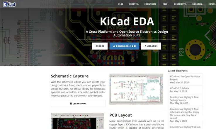
What Is a Kicad ?
KiCAD is a widely used open-source software that facilitates the design of electronic schematics and the subsequent transfer of these schematics to a PCB layout. One notable advantage of KiCAD is that it generates text files, which offer a straightforward approach for manual modification or the development of custom scripts. Moreover, KiCAD is a versatile software that supports multiple platforms including Microsoft Windows, OS X, and Linux.
Beneath its user-friendly interface, KiCAD comprises a collection of standalone software tools, meticulously integrated to form a cohesive system. These tools work harmoniously to provide an elegant and efficient solution for electronic design tasks.
| Program Name | Description | File Extension |
| KiCAD | Project manager | *.pro |
| Eschema | Schematic editor (both schematic and component) | *.sch, *.lib, *.net |
| CvPcb | Footprint selector | *.net |
| Pcbnew | Circuit board editor | *.kicad_pcb |
| Gerb View | Gerber viewer | All the usual Gerber |
| Bitmap2component | Convert bitmap images to components or footprints | *.lib, *.kicad_mod, *.kicad_wks |
| PCB Calculator | Calculator for components, track width, electrical spacing, color codes, and more | None |
| Pl Editor | Page layout editor | *.kicad_wks |
KiCad has gained significant maturity and reliability, making it an excellent choice for the successful development and ongoing maintenance of intricate electronic boards. Notably, KiCad surpasses any limitations related to board size, allowing seamless handling of complex designs. With the capacity to accommodate up to 32 copper layers, 14 technical layers, and 4 auxiliary layers, KiCad offers exceptional versatility.
One of KiCad’s strengths lies in its ability to generate comprehensive sets of files essential for the fabrication of printed circuit boards. These include Gerber files for photo-plotters, drilling files, component location files, and various other formats needed in the production process. As an open-source software licensed under GPL, KiCad becomes an optimal tool for projects aimed at fostering the development of electronic hardware with an open-source ethos.
Kicad PCB Definition
Kicad is a software utilized for Electronic Design Automation (EDA), specifically renowned for its capability to facilitate the design process of printed circuit boards (PCBs). With Kicad, users can seamlessly transition from schematic design to PCB layout.
Kicad provides a comprehensive and well-rounded environment for both schematic design and layout design stages. It empowers designers to create schematics with ease and precision. Furthermore, Kicad offers a range of features including generating a materials list, producing Gerber files, generating artwork, providing 3D views of the PCB, and component integration within the Kicad PCB environment. These features contribute to a holistic design experience, ensuring accurate and efficient realization of the circuit board design.
What Are The Features Of Kicad PCB ?
This software possesses distinct attributes that set it apart. The PCB undergoes a meticulous design process, ensuring a harmonious environment throughout each step. This process encompasses crucial stages such as PCB layout, schematic design, library editing, and Gerber file generation, all meticulously executed.
Some of the features of KiCad PCB include:
Schematic Capture: KiCad allows users to create and edit electronic schematics using a graphical interface.
PCB Layout: KiCad provides a powerful PCB layout editor that allows users to place components, route traces, and create custom footprints.
3D Viewer: KiCad has an integrated 3D viewer that allows users to view their PCB designs in 3D and check for any mechanical conflicts.
Design Rule Checking (DRC): KiCad includes a DRC tool that checks for design rule violations, such as minimum trace width and clearance, before sending the design for manufacturing.
Gerber/Excellon file generation: KiCad can generate Gerber and Excellon files required for manufacturing the PCB.
Library Management: KiCad has a built-in library management system that allows users to create and manage their own custom component libraries.
Multi-platform support: KiCad is available for Windows, Linux, and Mac OS, making it accessible to a wide range of users.
Community support: KiCad has a large and active community of users who contribute to its development, provide support and guidance to new users, and share their knowledge and resources.
The utilization of cross-platform software, programmed in C++, is a prominent characteristic of this system. A notable advantage is the ability to incorporate personalized components into your Kicad PCB. These custom components can be project-specific or installed for broader application.
Furthermore, Kicad PCB supports the utilization of third-party libraries, which offer additional component options. Notably, the configuration files are thoughtfully structured in plain text format, ensuring easy organization. Moreover, this software facilitates seamless integration with version control systems and enables the automation of component generation through scripting capabilities.
How Does kicard PCB work?
KiCad PCB works by allowing users to create a schematic diagram of their electronic circuit and then converting it into a physical layout for a printed circuit board (PCB). Here’s a general overview of how KiCad PCB works:
Schematic Capture: The first step is to create a schematic diagram of the electronic circuit using KiCad’s schematic editor. This involves selecting the components needed for the circuit and connecting them together using wires or buses. KiCad provides a wide range of built-in components, and users can also create their own custom components if needed.
Netlist Generation: Once the schematic is complete, KiCad generates a netlist, which is a list of all the connections between the components in the circuit. The netlist is used to create the physical layout of the PCB.
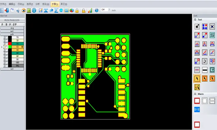
PCB Layout: The netlist is imported into KiCad’s PCB layout editor, where the components are placed onto the physical layout of the PCB and connected with traces and vias. The PCB layout editor allows users to customize the layout and routing of the PCB, including the placement of components, the routing of traces, and the creation of custom footprints for components.
Design Rule Checking (DRC): After completing the PCB layout, KiCad’s DRC tool is used to check for any design rule violations, such as minimum trace width and clearance. This helps ensure that the design is manufacturable and meets the specifications of the user’s chosen PCB manufacturer.
Gerber/Excellon File Generation: Once the PCB design has passed DRC, KiCad can generate Gerber and Excellon files that describe the layout of the PCB. These files are used by PCB manufacturers to create the physical board.
Overall, KiCad PCB works by providing a suite of tools for creating and designing electronic circuits, generating netlists and physical layouts, and checking the design for manufacturability. It is a powerful and versatile tool that is widely used by hobbyists, students, and professionals alike.
Getting Started with KiCad PCB
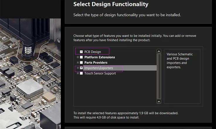
1. Download and install KiCad PCB: You can download the latest version of KiCad PCB from the official website. The installation process is generally straightforward and involves accepting the license agreement and selecting the components you want to install.
2. Create a new project: Once you’ve installed KiCad PCB, you can create a new project by clicking “File” > “New Project” and selecting “New Project” from the dropdown menu. You’ll then be prompted to give your project a name and select a location to save it.
3. Create a schematic: The first step in designing a PCB is to create a schematic. To do this, click “File” > “New” > “Schematic” and start adding components to your schematic. You can access the component libraries by clicking “Place” > “Component” and selecting the library you want to use.
4. Connect components: Once you’ve added all the components to your schematic, you can connect them by adding wires. To do this, click “Place” > “Wire” and click on the pins you want to connect. You can also add labels to your schematic by clicking “Place” > “Label”.
5. Create a PCB layout: Once you’ve completed your schematic, you can create a PCB layout from it. To do this, click “Tools” > “Annotate Schematic” to assign footprints to your components, and then click “Tools” > “Update PCB from Schematic” to create the PCB layout.
6. Place components: Once you’ve generated the PCB layout, you can start placing components on it. To do this, click “Place” > “Footprint” and select the component you want to place. You can then drag the component to the desired location on the board.
7. Route traces: Once you’ve placed all the components, you can start routing the traces that connect them. To do this, click “Route” > “Interactive Router” and start clicking on the start and end points of the traces you want to create. KiCad PCB will automatically generate curved traces that follow the path of least resistance.
8. Export your design: Once you’ve completed your PCB design, you can export it to the appropriate file formats for manufacturing. To do this, click “File” > “Plot” and select the output format you want to use, such as Gerber files or a Bill of Materials (BOM).
Tips and Tricks for Using KiCad PCB
Here are some tips and tricks for using KiCad PCB:

Keyboard shortcuts: KiCad PCB has a number of useful keyboard shortcuts that can save you time and effort. For example, pressing “E” in the schematic editor will open the properties dialog for a selected component, while pressing “M” in the PCB layout editor will switch to the move tool.
Interactive router: The interactive router is a powerful tool that can save you a lot of time when routing traces on your PCB. It allows you to route traces by clicking on the start and end points, and automatically generates curved traces that follow the path of least resistance.
Custom footprints: If you can’t find a footprint for a particular component in KiCad PCB’s built-in libraries, you can create your own custom footprint using the Footprint Editor. This can be a bit time-consuming, but it’s worth it if you’re using a component that’s not widely available.
Importing and exporting files: KiCad PCB supports a wide range of file formats, so you can easily import and export files to and from other PCB design software. For example, you can import Eagle CAD files or export your KiCad PCB design to Gerber files for manufacturing.
Libraries: KiCad PCB has a number of built-in libraries for common components, but you can also download and add custom libraries if you need to use specific components that aren’t included in the default libraries.
Design rule checker: The Design Rule Checker is a tool that can help you ensure that your PCB design meets certain standards and guidelines, such as minimum trace width and clearance. It can save you a lot of time and effort in the long run by catching potential issues early on.
Why Use KiCad for Your PCB Design ?
KiCad provides numerous advantages for printed circuit board design, including:
Open-source: KiCad operates as an open-source PCB design platform, fostering a collaborative environment among developers and enabling partnerships. Users can engage with a global community of PCB manufacturers and designers.
Free of Charge: KiCad does not require any payment or subscription for its download and usage. However, users have the option to support the software through voluntary donations.
Cross-platform Compatibility: This PCB design software is compatible with MacOS, Linux, and Windows. Project files created on one operating system can seamlessly transfer to another, ensuring flexibility and convenience.
Open Part Libraries: KiCad offers publicly accessible component libraries that encompass comprehensive collections of schematic symbols, 3D models, and footprints. Contributors continually develop and expand the library, providing a wide variety of resources. Users can effortlessly download and incorporate these components into their designs, and they can also contribute their own footprints and symbols to the library.
Reliable and Extensible: With its predominantly C/C++ programming, KiCad delivers exceptional performance across different systems. Moreover, KiCad leverages the capabilities of users’ graphics cards to enhance the display of graphical elements. The software supports Python scripting, allowing users to extend its features and streamline workflows effectively.
What Are The Disadvantages Of Kicad PCB ?
While KiCad PCB is a popular and widely used PCB design tool, there are some potential disadvantages to consider:
Steep learning curve: KiCad PCB has a steep learning curve, especially for beginners who are new to PCB design. It can take some time to get familiar with the software and its various tools and features.
Limited community support: While KiCad PCB has a dedicated community of users and contributors, it may not have the same level of support and resources as some other PCB design tools. This can make it more difficult to find answers to specific questions or issues.
Limited 3D modeling capabilities: KiCad PCB’s 3D modeling capabilities are somewhat limited compared to some other PCB design tools. While it does have a 3D viewer, it may not be as advanced or flexible as other software options.
Limited collaboration features: KiCad PCB does not offer advanced collaboration features, such as real-time collaboration or version control. While it is possible to collaborate on projects using external tools, this can be more difficult and time-consuming.
Lack of built-in simulation tools: KiCad PCB does not have built-in simulation tools, which can make it more difficult to simulate and test your designs before manufacturing. However, there are external simulation tools that can be used in conjunction with KiCad PCB.
It’s worth noting that many of these potential disadvantages can be mitigated with experience and familiarity with the software, as well as by using external tools or resources to supplement KiCad PCB’s capabilities.
Future Developments and Potential Improvements
KiCad PCB has been steadily improving over the years, and there are several future developments and potential improvements on the horizon. Here are a few examples:
Improved user interface: KiCad PCB has undergone several UI updates in recent years, but there is still room for improvement. Future updates could include more intuitive and user-friendly interfaces, improved workflow, and customizable toolbars.
Improved 3D modeling: While KiCad PCB has a 3D viewer, there is potential for further development in this area. This could include more advanced 3D modeling capabilities, such as the ability to create and manipulate 3D models directly within the software.
Integration with cloud-based services: Cloud-based services are becoming increasingly popular in the PCB design and manufacturing industry. Future developments could include integration with cloud-based services, such as collaborative design platforms and cloud-based simulation tools.
Improved collaboration features: While KiCad PCB does offer some collaboration features, such as the ability to export and import designs from other software tools, there is potential for further development in this area. This could include real-time collaboration features, version control, and commenting and markup tools.
Improved simulation and analysis capabilities: While KiCad PCB does not have built-in simulation tools, there is potential for integration with external simulation and analysis tools. Future developments could include closer integration with simulation tools and more advanced simulation capabilities directly within the software.
As a result, there is significant potential for future developments and improvements in KiCad PCB, and these developments could help to further improve the software’s capabilities and make it even more valuable for PCB designers and manufacturers.
Final Thoughts
KiCad PCB is a robust and versatile software solution for PCB design, offering an array of features and capabilities that cater to the needs of both designers and manufacturers. While beginners may encounter a learning curve, once acquainted with its tools and functionalities, the software proves user-friendly.
KiCad stands out as an invaluable design software for printed circuit board professionals. Unlike other alternatives in the market, it offers the advantage of being freely accessible, enabling users to create their PCB designs in accordance with the processes outlined in the article. Additionally, for more intricate PCB designs, seeking assistance from experienced professionals, particularly for hobbyist designers, can be a prudent choice. Furthermore, companies like JarnisTech PCB & Assembly can provide comprehensive solutions to meet various PCB requirements.
In conclusion, KiCad PCB is a highly commendable choice for those seeking a powerful and versatile PCB design software that combines accessibility, customization, and a broad range of features and capabilities. Its usage can unlock significant potential in your design endeavors.
Related Posts:
1. Everything You Should to Know on Altium PCB Design Software
2. Which One Are the Best Auto-route PCB Software?
3. PCB Traces: The Critical Role of Traces in PCB Design and Manufacturing
4. ExpressPCB Design Tool: A Comprehensive Guide to Using ExpressPCB
5. Avoid These 5 Common PCB Design Mistakes
6. You Need to know the PCB Design Software: Eagle PCB
8. What Is the Difference Between Altium and Eagle?
9. How to Make a Arduino PCB – You Must to know Everything About It
10. EDA Design Software: Definition, Kinds and Important