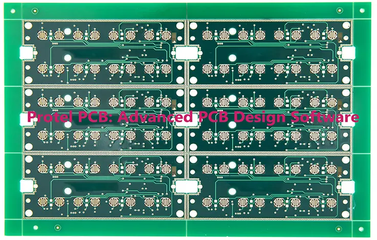
In the production of Printed Circuit Boards (PCBs), the utilization of software plays a pivotal role in tackling complex design challenges. PCB software assists engineers in various aspects, such as analog techniques, advanced schematic and circuit drawing, and adherence to design rules. Notable examples of PCB software encompass EDA board, Altium, Protel, and more. For the purpose of this discussion, we will focus on Protel PCB software. Let us proceed and delve into its features and benefits.
What is Protel PCB ?
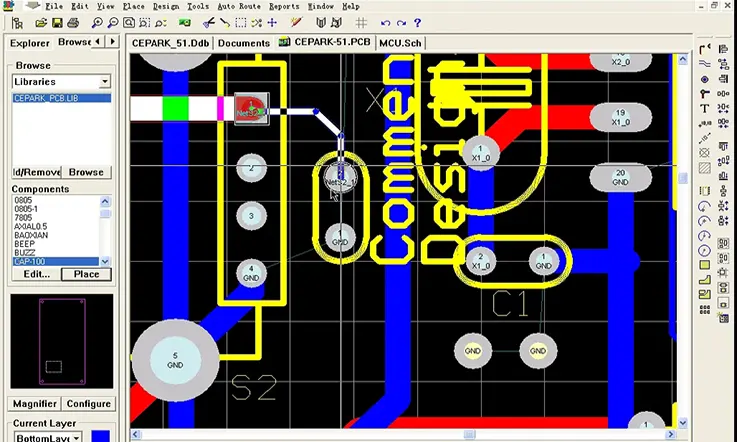
Printed circuit board manufacturers heavily rely on software for designing PCBs. The role of software in PCB production is crucial and cannot be overstated. Among the top-rated PCB design software options available, Protel PCB stands out as an exceptional choice. This software empowers electronic engineers to create efficient PCB layouts, facilitating the design process, the retrieval of previous board designs from PCB archives, and the verification of circuit schematic designs.
In the realm of engineering, companies utilize PCB design software for the development of PCBs. Numerous software solutions cater to the diverse needs of PCB engineers. Designing electronic circuits requires a combination of technical skills and engineering expertise. During the circuit board design phase, manufacturers must carefully select the appropriate circuit configuration. Hence, it becomes essential to leverage the right software for each specific design requirement. By utilizing suitable software tools, producers can optimize their design workflows and achieve successful outcomes in PCB development.
What is the Design Process of Protel PCB ?
In the design process, the utilization of a digital twin provides a comprehensive representation of the entire PCB system, encompassing substrates and multiple devices. The digital twin plays a crucial role in automating the verification of heterogeneous assemblies through various methods, including:
Substrate-level design rule checking (DRC): Ensuring adherence to design rules at the substrate level.
LVS (Layout versus schematic): Comparing the PCB layout with the corresponding schematic to validate their consistency and accuracy.
LVL (Layout versus layout): Comparing different versions of layouts to detect any discrepancies or inconsistencies.
Parasitic extraction: Extracting and analyzing parasitic elements in the PCB design to accurately predict circuit behavior.
Thermal and stress analysis: Evaluating the impact of thermal effects and mechanical stress on the PCB system to optimize reliability and performance.
Testing: Providing a platform to simulate and conduct virtual testing of the PCB design for comprehensive evaluation and validation.
By leveraging the capabilities of a digital twin, designers can enhance the efficiency and reliability of their PCB systems, while significantly reducing the reliance on manual verification processes.
Features of Protel PCB
Protel holds the distinction of being one of the initial PCB software specifically developed for personal computers. Throughout its evolution, it has consistently pioneered inventive tools that prove valuable across all stages of the PCB design process. Undergoing a transformation and currently known as Altium Designer, it has amassed over three decades of extensive experience in creating exemplary PCB designs. This software encompasses a wide range of features, which encompass:
Advanced Route and Place Tools
Protel boasts exceptional reroute and place tools, which constitute integral components of its design system. In the current iteration as Altium Designer, these tools have been further advanced and refined. With the aid of smart placement algorithms, designers can effortlessly position and organize their components, optimizing overall design efficiency.
The software also presents intelligent routing tools, enabling designers to expedite PCB routing processes. Furthermore, the inclusion of a native 3D environment empowers users to verify component placement using imported mechanical design data. Real-time adjustments to component positioning within the 3D workspace are also facilitated. Notably, the software has undergone significant enhancements to its core layout functionality, equipping designers with cutting-edge tools required for modern PCB design
Improved Utilities and Functionality
Protel PCB empowers designers to maintain a competitive edge by offering notable advantages. The software accelerates the routing of circuit board tracks, allowing for faster design iterations. An invaluable feature is the inclusion of Active BOM, which enables designers to directly assess crucial component data and seamlessly integrate component selection into the PCB layout process. This capability streamlines the design workflow and ensures efficient decision-making, ultimately contributing to enhanced competitiveness in the industry.
Unified Interface
Protel PCB software is purposefully crafted to provide engineers and designers with a robust platform for creating exceptional designs. It offers a comprehensive range of advanced design tools that are indispensable for achieving high-quality designs. The user interface is intuitively designed, ensuring ease of use for both seasoned professionals and newcomers to the field. This user-friendly nature allows users of all expertise levels to leverage the software effectively, thereby facilitating the creation of outstanding designs.
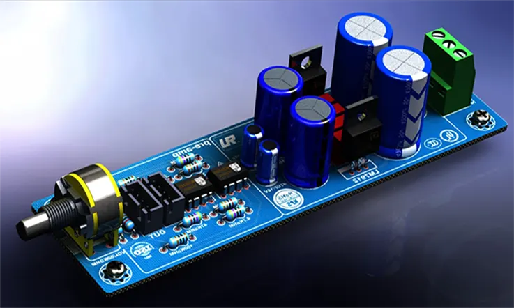
3D Visualization
Another notable feature offered by Protel PCB, now upgraded to Altium Designer, is its powerful 3D functionality. This feature empowers engineers and designers to effectively interact with and visualize their designs in a clear and comprehensive manner. The software provides advanced layout tools that facilitate precise routing and component placement, minimizing errors during the design process. By utilizing the 3D capabilities, users can inspect their designs from multiple perspectives, making it easier to identify and rectify any potential issues. Additionally, the software allows for seamless adjustment of component placement based on imported mechanical data, ensuring optimal design integration and compatibility.
Customer Interaction Use Case
The Protel design system facilitates effective customer interaction for designers. It offers practical use cases that enable seamless engagement with customers. One such capability is the ability to keep customers informed about the design progress by sharing snapshots of the work. Designers can conveniently share these snapshots on various devices, fostering clear and transparent communication with their customers. This feature promotes collaboration and ensures that customers are actively involved in the design process, leading to enhanced satisfaction and a stronger working relationship.
Advantages and Disadvantages of Protel PCB
Advantages
Protel PCB is a specialized software catering to the needs of engineers. This software offers numerous advantages, which are detailed below:
User-friendly: Protel PCB caters to the needs of both experienced professionals and beginners due to its user-friendly nature, characterized by ease of understanding and utilization. The software encompasses an array of tools, exporters, importers, and other functionalities that are accessible to designers of any level of expertise. In contrast to alternative PCB software options, Protel demonstrates a notable emphasis on user-friendliness through its intuitive design system. Alongside its ease of use, the software offers a comprehensive suite of tools, design templates, and an extensive component library, further enhancing the convenience and efficiency of the design process.
Reduces design complexity: Protel PCB is a software solution that streamlines the intricate nature of design processes. It employs a schematic as a starting point, enabling users to carefully choose appropriate components. The software offers the convenience of identifying and importing vendor components directly from the cloud into the design. Engineers can seamlessly create circuits on both multi-layer and single-layer boards. By employing Protel PCB, complex designs are simplified into logical iterations, enhancing efficiency and effectiveness in the design phase.
Saves Fee in Manufacturing: Protel PCB facilitates cost savings for designers by eliminating the need for physical prototypes during the production process. By utilizing software tools for quick virtual prototyping, manufacturers can efficiently allocate resources and labor to develop a cost-effective model of the final product.
Disadvantages
Protel PCB is a feature-rich software that provides numerous advantages for creating printed circuit boards. However, it is important to consider certain limitations associated with its use.
The software presents a wide array of features, which can sometimes lead to challenges in terms of navigation and ease of use. Users may find it initially overwhelming to navigate through the extensive feature set.
Furthermore, there have been reported instances of extended startup durations and slow file access, potentially impacting the overall efficiency of the design process.
Some users have found that the default configurations offered by Protel PCB could be ineffective in meeting their specific requirements, necessitating customizations.
An important limitation to note is the absence of simulation options within the software, which can limit the ability to perform detailed simulations and validate the design.
Another constraint is the limited level of element and user interface customization available. This might restrict users in tailoring the software to their preferences and workflow.
Additionally, the subscription cost of Protel PCB has been regarded as expensive by some users, which could pose financial constraints for individuals or smaller design teams.
While Protel PCB offers significant advantages, it is essential to be aware of its limitations and assess whether they align with specific design needs and financial considerations.
Why Protel PCB is the Best PCB Design Software ?
In the realm of PCB design tools, there are various options available. However, if you seek a comprehensive and unified experience along with a range of unique features, Protel PCB emerges as the ideal choice. The following reasons highlight the benefits of selecting Protel PCB over alternative PCB design tools:
Unification
To address the intricacies involved in technical Printed Circuit Board (PCB) designs, utilizing a unified platform such as Protel PCB can be highly beneficial. Through its unified design approach, the software provides one interface and data model, offering limitless possibilities for all PCB design requirements.
By embracing the unified design environment, users gain the ability to seamlessly handle various aspects of circuit board designs, encompassing schematics, harness designs, PCB layouts, and documentation. This integrated approach facilitates the smooth integration of the Protel PCB/Altium Designer software into every stage of the electronics design process, from conceptualization to manufacturing.
The unification of the design process extends beyond the designs themselves, as it encompasses comprehensive support for unified data models. This entails a cohesive data model that enables effortless access to harness designs, schematics, and layouts. Moreover, it allows for flexible manipulation of detailed data, including harness designs, schematics, simulations, layouts, and multi-board configurations.
Excellent Parts and BOMs Management
One of the prominent features of Altium Designer is its efficient management of parts and components required for the design process.
To begin with, the software offers a Manufacturer Part Search feature, allowing users to easily search and locate components from a comprehensive list of manufacturers. This feature streamlines the process of sourcing the necessary components for the design.
Furthermore, Altium Designer incorporates a remarkable feature called Real-Time BOM Management with ActiveBOM, which holds significant importance. This dedicated feature is specifically designed to assist circuit designers in effectively sourcing component data, managing these components, and facilitating access to suppliers directly from within the Altium Designer interface. This integrated functionality optimizes the component management process and enables seamless collaboration with suppliers.
Protel PCB Supports Interactive Routing
The Altium Designer PCB design software offers comprehensive support for interactive routing, enabling real-time routing of electronic components. This feature allows users to dynamically route components, enhancing the efficiency and flexibility of the design process.
Furthermore, Altium Designer provides interactive routing capabilities that offer multiple routing options for these components. Users can choose from a range of routing methods, including but not limited to the following:
Automatic Routing: Allows for automated routing based on predefined rules and constraints.
Manual Routing: Provides complete control over routing paths, allowing users to manually create and adjust traces.
Differential Pair Routing: Enables precise routing of differential pairs, ensuring signal integrity and minimizing cross-talk.
These interactive routing features empower users to achieve optimal routing solutions that meet their specific design requirements with ease and precision.
3D Routing
Altium Designer/Protel PCB offers an advanced feature called 3D Routing, which enables the seamless integration of mechanical and electrical requirements within a single solution.
With this capability, users can effortlessly incorporate and integrate standard Surface Mount Technology (SMT) footprints from the component libraries. Additionally, the connectivity and schematic design of the boards can be driven through the utilization of the schematic design.
This sophisticated functionality empowers users to optimize their design process, harmonizing the mechanical and electrical aspects for a more efficient and effective PCB design solution.
Why Choose JarnisTech as Your the best Protel PCB Manufacturer ?
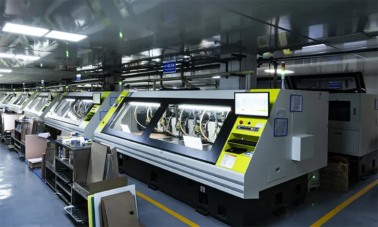
Choosing the most suitable company to represent one’s interests can be a challenging task, even when individuals possess a clear understanding of their requirements for Protel PCB in their circuit designs. Cooperation with selected Protel PCB suppliers and manufacturers is essential in ensuring that the boards align with all specifications, facilitating a successful product launch. This commitment to meeting customer needs fosters trust and positions us as the preferred Protel PCB manufacturer.
When individuals discover relevant information on company websites and reviews, it instills confidence in their decision-making process, enabling them to select the ideal enterprise to fulfill their requirements. Recognizing the paramount value of experience in any paid product or service, we have adapted to changing times while consistently delivering exceptional goods. Our company’s accreditation, coupled with the quality services and products showcased on our websites, substantiates our capabilities beyond words.
How do You Avoid Common Mistakes in Protel PCB Design ?
Ensuring high-quality layout circuit designs is crucial for optimal functionality of PCB components in Protel circuit design software. However, many engineers encounter difficulties in selecting the most suitable layout, which can lead to inefficient performance, particularly with devices featuring smaller pitch and higher pin counts.
Fortunately, there are effective solutions to overcome these challenges. For example, manufacturers can opt for PCBs with a reduced number of components. By minimizing the number of elements on the board, the PCB footprint is reduced, resulting in improved functionality. This approach allows for closer proximity between components, enhancing overall circuit performance. By implementing strategic design choices, engineers can mitigate the potential drawbacks associated with complex layouts and achieve superior circuit design outcomes.
Final Words
Protel PCB is a powerful and widely-used software tool for PCB design. It offers a comprehensive set of features and capabilities that make it a valuable tool for both beginners and experienced designers. Its user-friendly interface and intuitive design flow make it easier to create and modify PCB layouts. Protel PCB also provides advanced functionalities for design rules and constraints, simulation and verification, and generating manufacturing outputs.
One of the strengths of Protel PCB is its ability to streamline the PCB design process. It allows users to efficiently place components, route traces, and validate designs, helping to reduce errors and ensure electrical performance. The software’s simulation and verification tools enable designers to analyze and fine-tune their designs before sending them for manufacturing.
Protel PCB’s support for generating manufacturing outputs, such as Gerber files and assembly documentation, simplifies the transition from design to manufacturing. This feature ensures that the designed PCBs can be accurately produced by manufacturers while meeting industry standards.
Overall, Protel PCB is a reliable and feature-rich PCB design tool that offers a balance of functionality, usability, and efficiency. It continues to be a popular choice among PCB designers and contributes to the development of high-quality electronic products.
Related Posts:
1. Everything You Should to Know on Altium PCB Design Software
2. Which One Are the Best Auto-route PCB Software?
3. PCB Traces: The Critical Role of Traces in PCB Design and Manufacturing
4. ExpressPCB Design Tool: A Comprehensive Guide to Using ExpressPCB
5. Avoid These 5 Common PCB Design Mistakes
6. You Need to know the PCB Design Software: Eagle PCB
7. Kicad PCB: How to Understand It?
8. What Is the Difference Between Altium and Eagle?
9. How to Make a Arduino PCB – You Must to know Everything About It
10. EDA Design Software: Definition, Kinds and Important
11. Designing a PCB Layout: Everything You Need to Know
12. PCB Design Tips