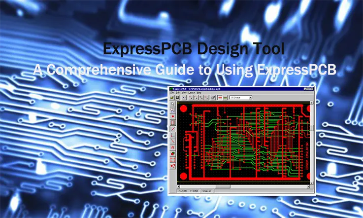
As a PCB designer, one often encounters the intricate nature of circuit design and occasionally wishes for a software solution that could simplify the process while reducing shipment time. Well, the wish has now become a reality with ExpressPCB.
ExpressPCB empowers PCB designers to effortlessly create schematic designs and generate PCB layouts. What sets it apart is its remarkable shipping speed, with a minimum turnaround time of five days, whereas other providers may take anywhere from 10 to 15 days. This impressive reduction in shipment time is complemented by a software that streamlines complexity, resulting in cost savings as well.
In this comprehensive guide, we will delve into the fundamentals of ExpressPCB, including an introduction to the software and a step-by-step tutorial on how to export Gerber files. Additionally, we will provide valuable insights from ExpressPCB users who have shared their experiences with the platform.
Prepare to embark on a journey through the world of ExpressPCB, where complexity is simplified, shipment time is minimized, and costs are optimized. Let us now proceed with the guide, unlocking the potential of this remarkable software.
Introduction to Express PCB
Express PCB is a software tool used for designing printed circuit boards (PCBs). It provides a user-friendly interface and a streamlined workflow, making it suitable for beginners and hobbyists who are new to PCB design. With Express PCB, you can create schematics, place components, route traces, and generate manufacturing files necessary for PCB fabrication.
Express PCB is known for its simplicity and ease of use. It offers a straightforward approach to PCB design without overwhelming users with complex features and options. This makes it a popular choice for quick prototyping, small projects, and educational purposes.
Benefits and Features of Express PCB:
User-Friendly Interface: Express PCB features a simple and intuitive interface that makes it easy to navigate and understand. The toolbar, menus, and project explorer are designed to provide quick access to essential functions and components.
Rapid Prototyping: With Express PCB, you can quickly transform your circuit ideas into physical PCB designs. Its streamlined workflow allows for faster iterations and prototyping, reducing the time required to bring your projects to life.
Component Library: Express PCB includes a built-in library of commonly used components, such as resistors, capacitors, ICs, connectors, and more. This library simplifies the process of selecting and placing components on the board, saving you time and effort.
Design Rule Checking (DRC): Express PCB performs automatic design rule checks to ensure that your PCB design meets specific manufacturing constraints and specifications. It helps identify potential errors or violations early in the design process, allowing you to make necessary adjustments.
Gerber File Generation: Express PCB can generate Gerber files, which are the standard file format used by PCB manufacturers to fabricate PCBs. These files contain all the necessary information about the PCB layers, traces, pads, and holes.
Cost-Effective: Express PCB offers a free version of its software, allowing users to create simple PCB designs without any licensing costs. This makes it an attractive option for hobbyists and those on a tight budget.
Overview of the PCB Design Process:
The PCB design process typically involves the following steps:
1. Schematic Design: Create a schematic diagram of your circuit, defining the connections between various components and their electrical relationships.
2. Component Placement: Place the components on the PCB layout, considering factors such as component clearance, signal integrity, and thermal considerations.
3. Routing: Connect the components through traces, carefully routing signals to avoid interference and maintain proper signal integrity.
4. Design Rule Checking: Run a design rule check to ensure that your design meets manufacturing constraints, such as minimum trace width, spacing, and clearance requirements.
5. Gerber File Generation: Generate the necessary manufacturing files, including Gerber files, drill files, and assembly files, to communicate your design specifications to the PCB manufacturer.
6. PCB Fabrication: Send the generated files to a PCB manufacturer for fabrication. The manufacturer will use these files to produce the physical PCBs based on your design.
Express PCB simplifies these steps by providing a user-friendly interface and automating certain aspects of the design process, allowing you to focus on the core aspects of your PCB design.
In the following sections, we will delve deeper into each aspect of using Express PCB, from installation and project setup to component placement, routing, and generating manufacturing files.
Installing Express PCB
Installing Express PCB is a straightforward process. Here is a step-by-step guide to help you install Express PCB on your computer:
System Requirements
Before you begin the installation, make sure your computer meets the minimum system requirements for running Express PCB. These requirements may vary depending on the version of Express PCB you are installing. Check the official documentation or the system requirements provided by Express PCB for the specific version you are using.
Downloading the Software
Visit the Express PCB website or the official download page to obtain the installation package. Look for the appropriate version of Express PCB that matches your operating system (Windows) and download the installer file to your computer.
Running the Installer
Locate the downloaded installer file on your computer and double-click on it to run the installation wizard. If prompted by the operating system’s security features, confirm that you want to proceed with the installation.
Accepting the License Agreement
The installation process begins with displaying the End-User License Agreement (EULA). Read through the agreement carefully and if you agree to the terms, click on the “I accept the agreement” or similar button to proceed with the installation.
Choosing the Installation Location
The installer will present you with the option to choose the installation location for Express PCB. You can either accept the default location or select a different directory where you want the software to be installed. Once you have made your selection, click on the “Next” or “Install” button to continue.
Selecting Additional Components (if applicable)
Depending on the version of Express PCB you are installing, you may be given the option to choose additional components or features to be installed along with the main software. Select the desired options, or if there are no additional components, skip this step by clicking on the “Next” or “Install” button.
Installing
The installer will now proceed to install Express PCB on your computer. It may take a few moments to complete the installation process. You may see a progress bar or indicator showing the installation progress.
Completing the Installation
Once the installation is finished, you will see a completion message or prompt indicating that Express PCB has been successfully installed on your computer. At this point, you may be given the option to launch the software immediately. If not, you can close the installer.
Launching Express PCB
To start using Express PCB, locate the software’s shortcut icon on your desktop or in the Start menu. Double-click on the icon to launch the application.
Activation and Licensing (if required)
Depending on the version of Express PCB you are using, you may need to activate and license the software. Follow the instructions provided by Express PCB to activate your copy of the software. This usually involves entering a license key or registering your account.
That’s it! You have now successfully installed Express PCB on your computer. You can now start exploring the software and begin creating your PCB designs.
Navigating the User Interface
Navigating the user interface of Express PCB involves understanding the layout, toolbars, menus, project explorer, library browser, and customization options. Here’s a breakdown of the key components:
Main Window Layout
The main window of Express PCB consists of various sections. It typically includes a workspace where you design your PCB layout, menus and toolbars for accessing different features and functions, and panels for displaying information, such as the project explorer and library browser.
Toolbars and Menus
Express PCB provides toolbars and menus to access various commands and functions. The toolbars typically contain icons representing common operations like opening, saving, zooming, placing components, routing traces, etc. The menus offer more comprehensive access to functions categorized under different menu items, such as File, Edit, View, Tools, and Help.
Project Explorer
The project explorer is a panel that displays the hierarchy of your project. It shows the project name, folder structure, and files associated with the project. You can use it to organize your project files and easily switch between different design files.
Library Browser
The library browser allows you to manage and access component libraries. It displays a list of available libraries and their contents. You can browse through the libraries, search for specific components, and add them to your project.
Setting Preferences and Customization Options
Express PCB provides options to customize the user interface and configure various settings to suit your preferences. You can access these options through the Preferences or Settings menu. Here, you can adjust settings related to units, grid spacing, colors, shortcuts, and more.
It’s important to spend some time familiarizing yourself with the user interface of Express PCB by exploring the different sections, menus, and toolbars. This will help you navigate efficiently and access the necessary functions for designing your PCB layout.
Creating a New PCB Project
Creating a new PCB project in Express PCB involves a few steps to set up the project parameters, define the board size and layers, and manage the components and libraries. Here’s a guide to creating a new PCB project:
Launch Express PCB
Start by launching the Express PCB software on your computer. Ensure that you have installed the software correctly.
Start a New Project
In the main menu, go to “File” and select “New” or use the corresponding toolbar icon to start a new project. This will open a blank project window.
Configure Project Parameters
In the project window, go to the “Project” menu or toolbar and select “Project Options” or “Properties.” Here, you can configure various project parameters such as the project name, description, author, revision, and date. Fill in the necessary details for your project.
Define Board Size and Layers
In the project window, go to the “Project” menu or toolbar and select “Board Layout.” This will open the PCB layout editor. In the editor, define the board size by specifying the width and height of the PCB. You can also set the number of layers you want to use for your design. Adjust these parameters according to your requirements.
Manage Components and Libraries
To manage components and libraries, go to the “Library” menu or toolbar and select “Component Manager” or “Library Manager.” In the component manager, you can add, remove, or edit components for your project. You can also create custom components or import components from existing libraries. In the library manager, you can manage your component libraries, add new libraries, and specify the location of your library files.
Save the Project
Once you have set up the project parameters, board size, and component libraries, it’s essential to save your project. Go to the “File” menu and select “Save” or use the save toolbar icon. Choose a location on your computer and provide a name for your project file. Saving the project file ensures that your progress is saved and can be easily accessed in the future.
You have now created a new PCB project in Express PCB. You can start designing your PCB layout by placing components, routing traces, and configuring other design elements. Remember to save your work regularly to avoid any data loss.
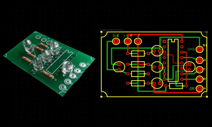
Designing the PCB Layout
Designing the PCB layout is a crucial step in the PCB design process. Express PCB offers a range of tools and features to help you create an efficient and functional layout. Here are the key steps involved in designing the PCB layout:
Placing Components on the Board:
Start by placing the components on the board. You can either select components from the built-in library or create custom components if necessary. Use the drag-and-drop functionality to position the components in the desired locations on the board.
Connecting Traces and Routing:
Once the components are placed, you need to establish connections between them by routing traces. Use the routing tools provided by Express PCB to draw traces between the component pins. Ensure that you follow design rules and guidelines to maintain signal integrity and avoid interference.
Adding Vias, Pads, and Through-Hole Components:
Depending on your design requirements, you may need to add vias, pads, and through-hole components. Vias allow you to create connections between different layers of the PCB. Pads are used to create landing areas for surface-mounted components, while through-hole components require holes to accommodate their leads.
Defining Power and Ground Planes:
To ensure proper power distribution and minimize noise, it’s often beneficial to include power and ground planes in your PCB design. Express PCB provides tools to define these planes and establish connections to power and ground pins of the components. This helps in creating a solid reference for signal integrity and reducing electromagnetic interference.
Design Rule Checking (DRC):
After completing the layout, it’s essential to run a design rule check (DRC) to validate your design against predefined rules and constraints. Express PCB’s DRC feature examines your layout for potential errors, such as incorrect clearances, overlapping traces, or missing connections. Address any issues identified by the DRC to ensure a manufacturable and functional PCB design.
Throughout the design process, it’s important to consider best practices such as component placement strategies, signal integrity, and manufacturability. Efficient component placement minimizes signal interference and facilitates routing. Proper trace routing techniques, such as using differential pairs and avoiding sharp angles, help maintain signal integrity. Additionally, following design guidelines for manufacturability ensures that your design can be fabricated and assembled without issues.
Express PCB provides a user-friendly interface and a set of tools to simplify the PCB layout process. Take advantage of these features, and don’t hesitate to consult the software’s documentation or online resources for more detailed instructions on specific functions.
Generating Manufacturing Files
Generating manufacturing files in Express PCB involves creating the necessary files that are required by PCB manufacturers to fabricate your design. The most common manufacturing files include Gerber files and the Bill of Materials (BOM). Here’s an overview of the process:
Gerber File Generation:
Gerber files are the standard format used to describe the different layers of your PCB design. They contain information about copper traces, solder masks, silk screens, drill holes, and other relevant features. To generate Gerber files in Express PCB, follow these steps:
a. Open your PCB design in Express PCB.
b. Go to the File menu and select “Export”.
c. Choose the option for Gerber files or Gerber 274X.
d. Specify the output folder and file names for each Gerber layer.
e. Select the desired layers to include in the Gerber files, such as top copper, bottom copper, solder mask, silk screen, etc.
f. Adjust any additional settings or options as required.
g. Click on the “Export” or “Generate” button to create the Gerber files.
Once generated, you can provide the Gerber files to your PCB manufacturer for fabrication.
Bill of Materials (BOM) Generation:
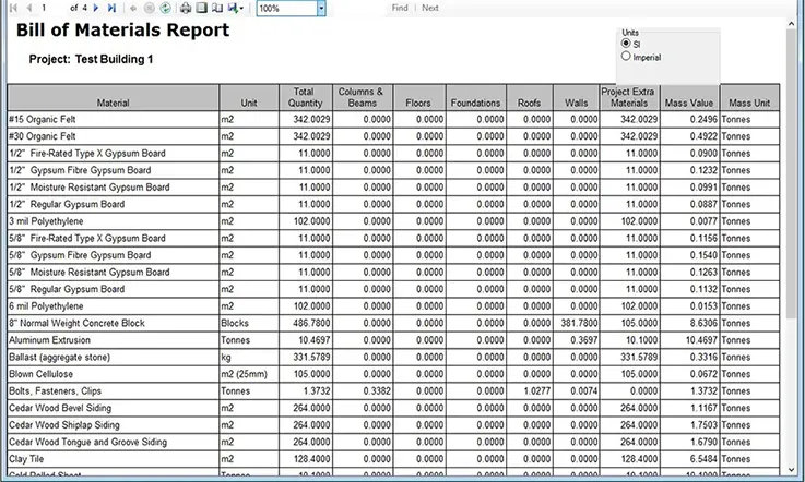
The Bill of Materials (BOM) is a document that lists all the components used in your PCB design, along with their quantities and reference designators. It helps the manufacturer identify and source the required components. To generate a BOM in Express PCB, follow these steps:
a. Open your PCB design in Express PCB.
b. Go to the File menu and select “Export”.
c. Choose the option for Bill of Materials (BOM).
d. Specify the output file name and location.
e. Adjust any additional settings or options, such as including attributes like part numbers or descriptions.
f. Click on the “Export” or “Generate” button to create the BOM file.
The generated BOM file can be provided to the manufacturer along with the Gerber files.
It’s important to note that the specific steps and options for generating manufacturing files may vary slightly depending on the version of Express PCB you are using. It’s recommended to refer to the software’s documentation or help resources for detailed instructions tailored to your version. Additionally, it’s always a good idea to communicate with your PCB manufacturer to ensure you provide them with the correct files and any additional requirements they may have.
Tips and Best Practices
Here are some tips and best practices to consider when working with Express PCB or any PCB design software:
Plan your design: Before diving into the PCB layout, spend time planning your design. Consider the components, their placement, power and ground connections, signal routing requirements, and any design constraints. Planning ahead will help you avoid mistakes and make the layout process smoother.
Component placement: Place components strategically to optimize signal integrity, minimize trace lengths, and ensure proper heat dissipation. Group related components together and place critical components first. Consider factors like component height, clearance, and accessibility for assembly and maintenance.
Trace routing: Follow good routing practices to minimize noise, crosstalk, and signal integrity issues. Use appropriate trace widths based on current requirements and impedance control. Keep traces as short and direct as possible and avoid sharp angles. Use ground and power planes whenever possible.
Design rule checking (DRC): Run the DRC feature to check for errors and rule violations. This helps ensure that your design meets the fabrication and assembly requirements. Pay attention to DRC warnings and resolve them to improve the overall quality of your design.
Use design layers effectively: Utilize different layers available in Express PCB to separate different types of signals, power and ground planes, and component outlines. This improves readability, simplifies debugging, and optimizes the PCB layout.
Document your design: Properly annotate and document your design to provide clear information to yourself and others involved in the project. Add reference designators, component values, and other necessary information to the PCB layout.
Test and verify: Before sending your design for fabrication, perform a thorough review and testing. Use the built-in simulation and analysis tools if available. Double-check component footprints, net connections, and design specifications to minimize the risk of errors.
Collaboration and version control: If you’re working in a team, establish a collaboration and version control system to manage design iterations, track changes, and avoid conflicts. This ensures smooth collaboration and prevents accidental overwriting or loss of work.
Seek community and online resources: Join PCB design forums, communities, or online platforms to connect with other designers, share knowledge, and seek advice. Many resources, tutorials, and design guidelines are available online to supplement your learning and help you overcome challenges.
Stay updated: Keep up with the latest updates, bug fixes, and new features released for Express PCB or any PCB design software you’re using. Regularly update your software to benefit from improvements and ensure compatibility with the latest industry standards.
Remember, practice and experience are key to becoming proficient in PCB design. Don’t be afraid to experiment, learn from mistakes, and continuously improve your skills.
Troubleshooting and Support
When working with Express PCB or encountering issues during the PCB design process, here are some troubleshooting tips and support options to consider:
Documentation and User Guides: Start by reviewing the official documentation and user guides provided by Express PCB. These resources often contain troubleshooting sections that address common issues and provide solutions.
Online Forums and Communities: Join online forums and communities dedicated to PCB design, such as the Express PCB user forum or general electronics design communities. Post your questions or search for existing threads related to your issue. Often, experienced users or even Express PCB representatives can provide guidance and solutions.
Knowledge Base and FAQs: Check the Express PCB website for a knowledge base or a frequently asked questions (FAQ) section. They often contain answers to common queries and troubleshooting steps for known issues.
Customer Support: If you’re unable to find a solution through online resources, reach out to Express PCB’s customer support. They can provide assistance and guidance for resolving specific issues related to their software. Contact information for customer support is typically available on the Express PCB website.
Software Updates: Ensure that you have the latest version of Express PCB installed. Software updates often include bug fixes and improvements that can address known issues. Check for updates regularly and install them as necessary.
Error Messages and Logs: Pay attention to any error messages or warnings generated by the software. These messages can provide valuable information about the cause of the issue. Take note of the specific error message or code and include it when seeking assistance. Additionally, check log files or error logs generated by Express PCB for additional details.
Double-Check Design Rules: If you’re encountering issues during the design or manufacturing file generation process, review your design rules. Ensure that your design adheres to the specified rules and constraints, such as trace widths, clearances, and component placement rules. Adjusting or relaxing certain design rules might resolve issues.
Hardware Compatibility: Check that your computer system meets the minimum requirements specified by Express PCB. Inadequate hardware resources can lead to software performance issues or instability. Verify that your operating system, processor, memory, and graphics capabilities are compatible with the software.
Reinstall or Repair: If you’re experiencing persistent issues that are not resolved through other troubleshooting steps, consider reinstalling or repairing the Express PCB software. This can help resolve any corrupted or missing files that might be causing the problem. Follow the instructions provided by Express PCB for reinstalling or repairing the software.
Remember to provide clear and detailed information when seeking support or troubleshooting assistance. Include relevant error messages, steps to reproduce the issue, and any specific circumstances surrounding the problem. This will help support personnel or community members better understand your situation and provide accurate guidance.
A Reliable Express PCB Manufacturing Service:JarnisTech
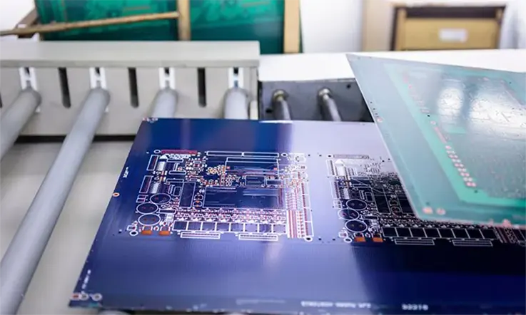
JarnisTech is dedicated to providing hobbyists and engineers worldwide with top-notch Quick Turn PCBs at competitive prices. Our expedited service ensures a swift turnaround time of just 24 hours, allowing you to meet tight project deadlines. To take advantage of our same day quick turnaround service, kindly ensure that your files are submitted before 9am. For further details regarding this service, we encourage you to reach out to us directly.
Engineers rely on JarnisTech due to our exceptional track record of delivering orders punctually and our commitment to manufacturing excellence. By opting for our accelerated service, you can significantly reduce the standard lead time of 2 weeks, enabling quicker prototyping of your critical PCBs. With our cost-effective pricing and unwavering reliability, you can minimize the risk of subpar PCBs while maximizing the return on investment for your PCB prototyping endeavors with JarnisTech.
Final Thoughts
This article has provided an overview of getting started with Express PCB, a popular software tool for designing printed circuit boards. We discussed the installation process, navigating the user interface, creating a new PCB project, designing the layout, performing design rule checks, generating manufacturing files, and shared some tips and best practices.
To sum up, mastering PCB design takes time and practice. Be patient with yourself, learn from your mistakes, and strive for continuous improvement. With dedication and a thirst for knowledge, you can become proficient in Express PCB and create high-quality PCB designs. Good luck on your PCB design journey!
Related Posts:
1. Everything You Should to Know on Altium PCB Design Software
2. Which One Are the Best Auto-route PCB Software?
3. PCB Traces: The Critical Role of Traces in PCB Design and Manufacturing
5. Avoid These 5 Common PCB Design Mistakes
6. You Need to know the PCB Design Software: Eagle PCB
7. Kicad PCB: How to Understand It?
8. What Is the Difference Between Altium and Eagle?
9. How to Make a Arduino PCB – You Must to know Everything About It
10. EDA Design Software: Definition, Kinds and Important