
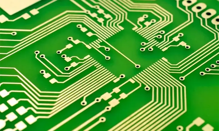
When it comes to printed circuit boards (PCBs), the term “trace” refers to the interconnected network of wiring, copper elements, insulation, and even fuses that collectively form the board’s structure.
In the majority of cases, when an electronic device exhibits a malfunction, it is highly likely that issues arise from inconsistencies within the PCB trace.
Are you frequently experiencing frustration and expending significant effort attempting to troubleshoot a circuit board, unsure of which calculations to perform?
If you are seeking a comprehensive guide that precisely outlines the calculations required (if necessary) for identifying trace resistance, you have come to the right place. This resource will provide you with all the essential information you need.
What Are PCB Traces?
A PCB trace refers to a collective network of wiring, copper elements, fuses, and insulation that form an integral part of a printed circuit board. It serves as a highly conductive path responsible for interconnecting various components such as ICs, capacitors, and resistors on the PCB.
To effectively conduct electricity, PCB traces require a material with high conductivity and stability. Copper is the most commonly used material for trace fabrication, although alternatives like gold and aluminum are also viable options.
The significance of PCB traces cannot be overstated, as inconsistencies or errors within them often lead to malfunctions in electronic devices. Therefore, meticulous attention to detail is crucial during the design phase, considering the PCB trace as a fundamental element of PCB fabrication.
When designing PCB traces, several essential parameters must be carefully considered. These parameters encompass trace width, trace thickness, trace resistance, trace current, and various other factors that contribute to the optimal performance and reliability of the PCB.
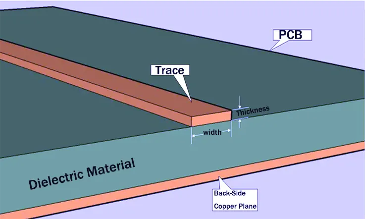
Thickness of a PCB Trace
The thickness of a PCB is a crucial aspect in its design, and electronic designers attach great importance to this factor. It significantly impacts the overall balance and functionality of the PCB. Neglecting the significance of thickness can lead to various issues with the circuit board’s performance.
In the present market, there are different types of PCB boards available. These include single-sided boards, double-sided boards, and multi-layered PCB boards. Each version of the printed circuit board has its own track thickness specifications. Generally, the PCB trace thickness ranges from 0.008 inches to 0.240 inches, providing a range of options to accommodate different design requirements.
Maintaining an appropriate track thickness is essential for ensuring the structural integrity and electrical performance of the PCB. It is a critical consideration that electronic designers carefully evaluate to guarantee optimal functionality and reliability of the circuit board.
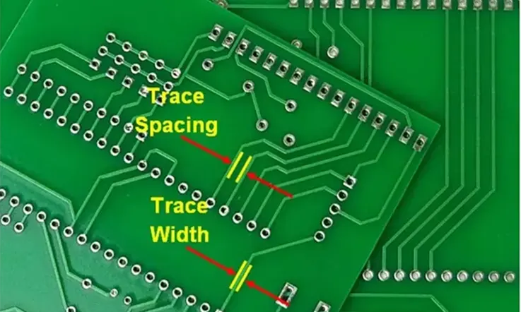
PCB Trace Width
Trace width is a fundamental and critical parameter in PCB design and layout. It plays a vital role in carrying currents through circuit boards while ensuring that trace temperatures remain below specified limits to prevent overheating.
Traces serve the purpose of conducting signals to and from the pins of soldered components on the circuit board, carrying varying amounts of current depending on the specific net. Certain signal traces may have unique electrical requirements that influence their size, necessitating careful regulation of trace widths to ensure accurate and efficient board manufacturing.
Typically fabricated from copper during the circuit board etching process, traces are subject to an aggressive etching process. Fabricators must exercise caution to prevent over-etching, which can result in traces being thinner than their intended widths.
Isolated traces on the board are susceptible to being more heavily etched compared to traces that are grouped together. This is due to the concentration of etching in a specific area. To mitigate this, it is advisable to slightly increase the width of isolated traces to prevent excessive etching. Over-etched traces pose a risk to the signal integrity of the circuit board, underscoring the importance of meeting target trace widths.
The weight or thickness of the copper being etched also warrants careful consideration, as traces with greater copper weight cannot be etched down as much as other traces due to their inherent thickness. Copper layers used in PCBs typically come in standard thicknesses, often measured in ounces per square foot (oz/sq ft) or Mil. Generally, thicker copper layers require narrower trace widths. For most PCBs, a common copper thickness is 35µm, equivalent to 1oz/square foot.
Trace widths can also impact the soldering processes employed during PCB assembly. Wide traces used for power and ground routing can act as heat sinks, resulting in uneven soldering temperatures and poor solder joints. This issue becomes particularly challenging when dealing with large components such as high pin-count ball grid arrays (BGAs) or surface mount connectors, as identifying and rectifying defects may require costly inspection and rework procedures.
Beyond the complexities associated with accurate trace width fabrication, it is crucial for the electrical performance of circuit boards. Trace widths play a critical role in maintaining both the signal and power integrity of the board, underscoring their significance in achieving optimal functionality and reliability.
PCB Trace Width Calculator
Trace width is a critical design parameter that significantly impacts PCB design. It is imperative to establish an appropriate trace width to facilitate the safe and efficient transportation of current without risking overheating or damage to the board. To assist in this process, an online tool is available for estimating the minimum trace width based on specific current requirements and the copper weight used. It is important to note that higher current demands necessitate thicker traces, whereas a thicker copper weight allows for the use of thinner traces. By leveraging this tool, designers can accurately determine the optimal trace width for their PCB design, ensuring the reliable and effective operation of the circuitry.
So, PCB Trace Resistance-What Is It and How To Use?
When designing printed circuit boards (PCBs), calculating and analyzing trace resistance is vital. All conductive materials exhibit inherent resistance, along with other parasitic characteristics.
While copper serves as the predominant PCB trace material, its composition and properties can vary. As circuit complexity increases, higher trace resistance can lead to several performance and reliability issues during PCB design and operation.
Carefully evaluating trace resistance based on factors like material quality, trace dimensions, and circuit current demands is crucial. This helps designers minimize overall trace resistance and its associated impacts, including resistive power losses, signal degradation, and component overheating. Proactively optimizing PCB trace resistance through simulation, calculations, and design choices results in more efficient, functional, and resilient circuit board layouts.
The below is the formula for resistance of a trace:
●Resistance = Resistivity*Length/Area*(1 + (Temp_Co*(Temp – 25)).
●Where, Area = Thickness*Width.
●A copper Thickness of 1 oz/ft^2 = 0.0035 cm.
●Copper Resistivity = 1.7E-6 ohm-cm.
●Copper Temp_Co = 3.9E-3 ohm/ohm/C.
●Voltage Drop is Current * Resistance.
●Power Loss is Current^2 * Resistance.
Something you need to know before calculating trace width:
Proper trace width calculation for printed circuit boards (PCBs) requires consideration of several key factors. The maximum current capacity is an essential input, as this will significantly impact the necessary trace width. Other key inputs include:
●Trace thickness (in mils or microns).
●Trace temperature (in Celsius), both the temperature during operation and ambient temperature.
●Desired voltage drop across the trace (in volts).
●Acceptable power dissipation (in watts).
By inputting these parameters into a trace width calculator, the appropriate trace width can be determined (typically measured in mils). The calculator will also output resulting values for trace resistance (in ohms), trace temperature (in Celsius), voltage drop (in volts), and power dissipation (in watts).
Careful evaluation of these inputs and outputs helps PCB designers determine optimal trace dimensions to handle required current levels, meet thermal constraints, and avoid excessive power loss across traces. This thoughtful trace width selection is crucial for overall PCB performance and reliability.
PCB Trace Current
The current-carrying capacity of a printed circuit board (PCB) trace refers to the maximum current that the trace can conduct without causing failure or overheating of electronic components on the board. The trace current capacity is primarily determined by the physical dimensions of the copper trace – namely the width and thickness.
Wider and thicker traces can safely conduct higher levels of current. Thinner and narrower traces are more resistive, generating more heat at high currents. Excessive temperatures can damage solder joints, degrade insulation, or permanently alter conductive properties of the copper trace.
Max Current calculation
First, calculate the area according to the following formula:
A = (T · W · 1.378 [mils/oz/ft2])
Then, calculate the maximum current:
IMAX = (k · TRISEb) · Ac
Where:
A is the cross-section area [mils2]
T is the trace thickness [oz/ft2]
W is the trace width [mils]
IMAX is the maximum current [A]
TRISE is the maximum desired temperature rise [°C]
k, b and c are constants. According to IPC-2221A Section 6.2, their values for inner layers are as follows:
k = 0.048 b = 0.44 c = 0.725 [4]
Proper PCB design requires matching trace widths and thicknesses to anticipated current levels. Understanding the relationship between trace dimensions and current capacity is essential to ensure all conductive traces have appropriate capacity for their circuit location. This prevents trace overheating and avoids damage to connected components.
PCB Trace Width Vs PCB Trace Current
When designing a printed circuit board (PCB), the components are connected to various points through copper electrical traces. The proper functioning of the PCB traces depends on their width. As electrons pass through the copper, they generate thermal energy. The temperature of the board can be controlled by adjusting the trace width. Wider traces allow electricity to flow more smoothly.
While default trace widths may be used initially in a PCB design, the board may benefit from a custom trace width instead of the default. Current carrying capacity is a key factor when selecting an appropriate trace width. Using a width suited for the expected current levels can help manage heat generation and ensure reliable performance.
| PCB trace width | PCB trace current |
| A trace width of 6mil (or 0.152mm) is the bare minimum for most factories. The manufacturing method (etching) and desired output are responsible for this restriction. We utilize 10-12 mil (0.254-0.3 mm) traces to allow some wiggle room. | Less than five miles (0.005″) in width Lower than five-millimeter trace spacing. Holes for vias having a diameter of fewer than 8 micrometers. Sub-ounce or ounce-thickness traces (which equates to 1.4 mils) |
| Minimum PCB clearance (the clearance between any two wires) for general-purpose devices is 0.1 mm according to IPC 2221 standards. | This minimum PCB Trace Current spacing of 0.13 mm (or 5.1 mils) applies to power conversion components. |
| Trace width clearance on a PCB refers to the distance between adjacent traces and the width of the traces themselves. | Whereas clearance refers to the smallest distance between two conductor traces in the air, creepage refers to the shortest distance of conductor traces on a PCB along the surface of the insulating material. |
Considerations For PCB Traces
The design and layout of a printed circuit board (PCB) are crucial factors that directly impact the production cost and operational efficiency of the board. A well-thought-out layout design not only helps to save production costs but also ensures the effective functioning of the circuit board. Neglecting proper layout considerations can lead to issues such as electromagnetic interference, circuit failures, and other serious problems. Therefore, it is essential to take practical considerations into account when designing the layout, including material and component quality, component placement, power and heat management, and the limitations of the circuit board, in order to achieve a more rational layout and maximize its operational efficiency.
PCB trace spacing and width significantly affect the circuit board in various ways, necessitating attention to the following four factors:
Electrical performance and signal integrity:
Typically, most tracks on the board have default width and spacing values. However, specific applications may require different dimensional widths or spacing. For instance, controlled impedance networks require precise calculation of PCB trace widths when employing layered board configurations. Sensitive and high-speed traces require sufficient spacing to prevent signal crosstalk. Depending on the circuit’s requirements, special trace width and spacing considerations may be necessary, such as reducing the default PCB trace width in narrower areas.
Power and ground routing:
To accommodate higher current transmission, the paths for power sources and grounds should be wider. Thin traces are prone to heating up and can be easily damaged by high-power currents. Additionally, the internal wiring paths on the board should be wider than those on the outer layers to enhance heat dissipation. Minimizing trace length within the circuit board is crucial for reducing noise. When traces need to carry substantial current, appropriate spacing between them should be maintained to prevent arc formation.
PCB fabrication:
The fabrication process of circuit boards is influenced by trace width. Larger trace widths, such as 20 mil traces compared to 3 mil traces, offer greater tolerance for metal loss during fabrication. This implies that larger PCB trace widths are more favorable for the manufacturing process. The weight of copper used in the PCB fabrication also significantly impacts trace widths. Excessive copper weight makes it challenging to carve thin trace widths on the circuit board, emphasizing the importance of considering the design of PCB copper traces.
Circuit board assembly:
Excessively wide PCB trace widths can negatively affect the soldering process. Wide traces used for ground grids and power supplies can lead to uneven heating and blockage of soldering points.
By carefully considering these factors, designers can ensure that the PCB layout meets the necessary electrical, fabrication, and assembly requirements, promoting optimal performance and reliability of the circuit board.
Best Advice For PCB Trace Design
Designing Printed Circuit Board (PCB) traces effectively is essential to performance, reliability, and manufacturability of your board. Here are some key points to consider when designing your PCB traces:
Trace Width: The width of your traces should be sufficient to handle the current that will be flowing through them. There are online calculators that can help you to determine the appropriate width based on the current and the thickness of copper.
Trace Spacing: Keep enough space between traces to prevent cross-talk and short circuits. This is particularly important for high frequency signals.
Use 45 Degree Angles: Instead of using 90-degree angles, use 45-degree angles or curves. This helps to reduce signal reflections and electromagnetic emission.
Impedance Control: For high frequency signals, you’ll need to control the impedance of your traces. This involves careful consideration of the trace width, thickness, substrate material, and distance to the ground plane.
Power and Ground Planes: Use power and ground planes wherever possible. This provides a low-inductance path for power and return signals, which can improve signal integrity and reduce emissions.
Differential Pairs: If you’re using differential signaling, make sure to route the two traces of each pair close together and keep them the same length to maintain the differential impedance.
Avoid Loops: Loops can act as antennas and emit electromagnetic radiation, which can cause EMI problems. Always try to route traces in a way that avoids creating loops.
Thermal Considerations: Traces can heat up if they carry a lot of current. Make sure to consider thermal effects and ensure your design can handle the heat.
Layer Stacking: In multi-layer PCBs, carefully consider the stack-up of your layers. Adjacent signal layers should usually be routed in perpendicular directions to reduce crosstalk.
Test Points: Consider adding test points in your design for debugging and testing. They should be located on meaningful signals and are typically just exposed areas of copper.
Remember that these are general guidelines and the specific requirements of your design may necessitate different approaches. Always validate your design with appropriate simulation tools and prototyping.
How To Repair PCB Traces?
Acquiring knowledge on the process of repairing PCB trace issues holds significant importance, particularly when encountering problems such as display failure or unusual noise in the power supply unit. To effectively address these issues, the following detailed steps can be followed for PCB trace repair:
● Begin by identifying the location of the damaged trace on the PCB with precision.
● Utilize a cutting tool to carefully remove the damaged trace, exercising caution to avoid causing harm to nearby components.
● Clean the affected areas thoroughly until they exhibit the characteristic copper color, and proceed to apply solder to the exposed regions.
● Employ a cleaning paper towel or a solvent cleaning pen to meticulously clean the repair area. Additionally, apply flux to the existing track and utilize a soldering iron to facilitate the soldering process for both sections of the track.
● Select a suitable replacement wire that is in optimal condition and of an appropriate size.
● Apply a thin layer of solder (tinning) to the ends of the replacement wire.
● If the replacement wire is deemed suitable, remove the insulation from both ends and proceed to solder it in place.
● Initially, solder one end of the replacement wire, ensuring that a section of the new wire overlaps the existing trace by at least twice the width of the PCB trace. Secure the wire using tape, apply flux to the overlap, and solder the wire and trace together.
● Flexibly shape the wire according to specific requirements and needs.
● Securely attach the wire to the surface of the circuit board using tools such as tape or adhesive.
● Finally, solder the other end of the replacement wire, ensuring a strong and reliable connection.
● Upon completing the soldering process, finalize the repair procedure and thoroughly inspect the connection to ensure its normal functionality. Additionally, clean any remaining residue or stains diligently.
By adhering to these steps and maintaining a professional approach, one can effectively repair PCB trace issues, mitigating problems such as display failure or abnormal noise in the power supply unit.
What’s the role of PCB trace in PCB?
Effective management of impedance is crucial in maintaining the desired signal integrity for PCB traces. It involves adjusting the size and placement of traces to match the characteristics of the substrate material, ensuring that the signal intensity remains within an acceptable range. With the increasing switching rates of modern devices, engineers face challenges in dealing with signal integrity issues. Consequently, PCB traces cannot be treated simply as direct connections between two points; they must be treated as transmission lines to mitigate the impact on signal integrity, requiring impedance matching techniques. By adhering to sound design techniques and methods, many potential signal integrity concerns can be avoided or minimized.
The primary function of a PCB trace is to carry electrical current from the device, transmitting the signal to its intended receiver. Simultaneously, power must be delivered along the trace. However, to achieve optimal signal power, it is essential to establish impedance matching on the PCB. This ensures that as much of the driver’s power as possible reaches the receiver.
If the PCB layout stage does not pay careful attention, high-frequency signals will inevitably degrade as they propagate from the driver to the receiver. This degradation becomes evident in the form of distorted signals on an eye diagram, exhibiting varying amplitudes as they traverse from the signal source to the destination.
Conclusion
Having a comprehensive understanding of PCB trace routing is essential for achieving optimal board performance, reliability, and cost-effectiveness. It simplifies the PCB design and manufacturing process, making it crucial to acquire fundamental knowledge and skills in trace routing design. As a reputable PCB manufacturer, Jarnis Technology possesses extensive expertise in all aspects of circuit board knowledge. If you have any inquiries or require assistance regarding PCB traces, our team of experts at Jarnis Technology is readily available to provide you with the support you need. We are committed to delivering exceptional service and guidance to ensure your PCB trace routing meets the highest standards.
In addition, JarnisTech offers an instant quote service that caters to various PCB needs. We specialize in quick-turn PCB prototyping, PCB assembly, as well as medium and small volume PCB fabrication. Our services include a 24-hour lead time, prompt component quoting within 24 hours, and efficient prototype PCB assembly within 24 hours. We strive to meet your specific requirements for PCB fabrication and assembly while adhering to the highest industry standards.
For any inquiries or questions you may have, please don’t hesitate to contact us at [email protected]. We are dedicated to providing assistance and support, and we will be more than happy to assist you.
Related Posts:
1. Everything You Should to Know on Altium PCB Design Software
2. Which One Are the Best Auto-route PCB Software?
4. ExpressPCB Design Tool: A Comprehensive Guide to Using ExpressPCB
5. Avoid These 5 Common PCB Design Mistakes
6. You Need to know the PCB Design Software: Eagle PCB
7. Kicad PCB: How to Understand It?
8. What Is the Difference Between Altium and Eagle?
9. How to Make a Arduino PCB – You Must to know Everything About It
10. EDA Design Software: Definition, Kinds and Important