Introduction
High frequency PCBs (HFPCBs) are integral to the advancement of technologies in sectors like 5G, aerospace, and healthcare. As the demand for faster and more efficient electronic devices rises, designing these PCBs requires a sophisticated understanding of materials, design processes, and thermal management. Ensuring signal integrity at higher frequencies and maintaining performance across a range of conditions calls for precision manufacturing and expert engineering to meet the technical demands of modern electronics.
In this guide, we’ll explore the ins and outs of High Frequency PCBs—detailing their design, production, and testing processes. We’ll also highlight the ways manufacturers and designers can collaborate to tackle the challenges of working with these advanced circuits. Whether you’re involved in PCB engineering, medical device manufacturing, or sourcing high-frequency components, this article will equip you with the expertise needed to navigate this dynamic and complex field with confidence.
Key Principles of High Frequency PCB Design
When designing high-frequency PCBs, you’re walking a tightrope between theory and real-world application. Signals zooming from the MHz to GHz range demand a delicate touch when it comes to material choices and trace layout. To make sure your board doesn’t skip a beat, you’ll need to lock in on factors like signal quality, routing strategies, thermal control, and the right materials. All of these elements must be dialed in just right to avoid any hiccups. It’s a bit like tuning a high-performance engine—you’ve got to get everything firing on all cylinders.
Signal Integrity and Trace Routing in High Frequency PCB Design
Signal integrity is a primary concern in high-frequency PCB design, as even small imperfections in the circuit can result in signal degradation, leading to failures in communication, timing issues, or data corruption. The electromagnetic environment (EMI) also comes into play, where noise and interference must be mitigated at all stages.
Key factors that affect signal integrity in high frequency designs include:
●Trace Impedance: The impedance of PCB traces must be controlled to prevent reflection and signal loss. In high-frequency designs, even a slight mismatch between the transmission line impedance and the load impedance can cause reflections, leading to signal degradation.
●Trace Width and Spacing: The width of the traces and the spacing between them directly affect the impedance and signal quality. For high-speed signal propagation, traces need to be designed with precise measurements.
●Via Design: Vias introduce inductance and resistance into the signal path, impacting signal integrity. Minimizing via usage and optimizing via size and placement can drastically reduce performance losses.
Here’s a simple guide for calculating trace width based on different impedance values and frequency ranges:
| Trace Width (mil) | Impedance (Ohms) | Frequency Range (GHz) | Material | Loss Factor |
| 4 | 50 | 1-5 | FR4 | High |
| 6 | 75 | 5-10 | Rogers 4003C | Moderate |
| 8 | 100 | 10-20 | Taconic TLY-5 | Low |
The impedance control here is key for minimizing losses in high-frequency signal transmission. Understanding how these trace parameters interact at various frequencies can give you a significant edge in achieving robust performance.
Design for Low-Loss Materials in High Frequency PCBs
Choosing the right PCB raw materials for your high-frequency PCB is one of the most important decisions you can make. The dielectric constant (Dk) and dissipation factor (Df) of materials directly affect signal loss and overall signal integrity.
Low-loss materials ensure minimal signal attenuation, high thermal stability, and minimal dielectric heating. Here are some of the best materials for high-frequency designs:
●Rogers: A go-to material for high-frequency applications, especially RF and microwave circuits. Rogers offers low Dk and Df, making it perfect for 5G and military applications that require high-performance, low-loss characteristics.
●Taconic: Known for high-performance and low dielectric loss, Taconic is widely used in high-frequency communications and high-speed circuit applications.
●PTFE (Polytetrafluoroethylene): Common in microwave PCBs due to its low Dk and Df. It helps maintain signal integrity by resisting high-frequency signal attenuation.
Let’s take a look at the relative loss for various high frequency PCB materials:
| Material | Dielectric Constant (Dk) | Dissipation Factor (Df) | Loss at 10 GHz |
| Rogers 4350B | 3.48 | 0.0035 | Low |
| Taconic TLY-5 | 2.55 | 0.0040 | Moderate |
| PTFE | 2.2 | 0.0002 | Very Low |
Materials like Rogers and PTFE are highly recommended for signal integrity in high-speed designs and RF circuits.
Managing Heat in High-Frequency PCBs
As frequencies increase, the amount of power loss and heat generation in a circuit also grows. This can lead to thermal runaway, which degrades both signal quality and the longevity of the components. Managing heat in high-frequency PCB designs is a crucial aspect that shouldn’t be overlooked.
To effectively manage heat, consider the following methods:
●Thermal Via Design: Thermal vias act as the heat transporters within the PCB, redirecting heat from the outer layers to internal layers or heat sinks. Getting the placement and size right ensures efficient heat dissipation, preventing overheating and avoiding damage to the components. It’s like installing the perfect exhaust system in a car—if the pathways aren’t optimized, the system struggles, and the performance can take a hit. Precision here helps maintain both longevity and reliability in your design.
●Heat Sink Application: Attach heat sinks to components that generate substantial heat, especially in high-frequency power amplifiers or RF components.
●Copper Pouring: Copper pour, or the use of large copper areas to dissipate heat, is another method to help reduce thermal buildup.
Here’s a look at how different thermal via designs affect heat dissipation:
| Via Type | Thermal Resistance (°C/W) | Max Power Handling (W) | Cost |
| Standard Via | 15 | 0.5 | Low |
| Thermal Via | 10 | 1.0 | Moderate |
| High-Density Via | 5 | 2.0 | High |
Using high-density thermal vias or larger vias can significantly improve heat dissipation but may add to the cost.
Designing Multi-Layer Stack-Ups for High-Frequency PCBs
Designing multi-layer stack-ups for high-frequency PCBs involves a meticulous approach to impedance control, signal routing, and managing electromagnetic interference (EMI). The success of these designs is predicated on balancing electrical and thermal performance, optimizing layer organization, and using advanced materials to maintain the integrity of high-speed signals. Below, we break down key aspects that go into designing these high-performance stack-ups.
Layer Configuration for Impedance Control in High-Frequency PCBs
Impedance control is one of the most critical aspects of high-frequency PCB design, especially in applications that handle RF or microwave signals. The layer stack-up must be carefully configured to ensure that the PCB maintains consistent impedance, preventing signal reflection, and minimizing transmission loss. It’s kind of like making sure all the lanes on a highway stay the same width—if they don’t, things slow down or even crash. Get the impedance right, and your signals flow without a hitch, keeping everything in sync and running at peak performance.
Key Techniques in Layer Configuration-
1.Balanced Stack-Up: A balanced stack-up ensures uniform dielectric properties between layers, which is crucial for maintaining stable impedance. For example, in a 4-layer PCB, a typical configuration could be:
●Layer 1: Signal
●Layer 2: Ground
●Layer 3: Power
●Layer 4: Signal.
This configuration minimizes signal distortion, as the signal traces are positioned symmetrically around the ground and power planes.
2.Dielectric Thickness and Trace Width: The relationship between the trace width and the thickness of the dielectric material dictates the impedance of a signal trace. For example, a wider trace increases the surface area and lowers impedance, while a narrower trace increases impedance. Proper calculations are required to achieve the target impedance, typically 50 ohms for single-ended signals or 100 ohms for differential pairs.
3.Materials Selection: Materials with low dielectric constants (Dk) and low loss tangents (Df) are preferred. These materials help preserve signal integrity by reducing signal loss and ensuring that the signal travels at an appropriate speed.
Example Configuration: A stack-up for a high-frequency application like a 5G base station might look like this:
●Layer 1: Signal
●Layer 2: Ground (adjacent to signal layer for reduced noise)
●Layer 3: Power (for stable voltage supply)
●Layer 4: Signal This setup ensures efficient impedance control, minimizing signal reflections and power loss.
Impedance Control Design Guidelines-
| Trace Width | Impact on Impedance | Recommended Design Considerations |
| Wider Trace | Lowers impedance | For low-frequency signals |
| Narrower Trace | Increases impedance | For high-speed or high-frequency signals |
| Dielectric Thickness | Thinner = Higher Impedance | Adjust for specific signal needs |
| Material (Dk) | Lower Dk = Faster Signal Propagation | Use low-Dk materials like PTFE or Rogers |
Ground and Power Plane Integration
A well-designed ground and power plane setup in high-frequency PCBs helps reduce noise and improve the reliability of the circuit.Well-designed ground and power planes not only reduce noise but also ensure signal integrity by providing clear return paths for high-frequency signals. Without effective grounding, high-frequency designs are vulnerable to performance degradation due to noise and cross-talk.
Ground Plane Placement-
1.Proximity to Signal Layers: Placing ground planes immediately below signal layers reduces loop inductance, providing a direct path for returning currents. For example, in a 4-layer PCB, the ground plane is typically located right under the signal trace to ensure low inductive impedance.
2.Stitching Vias: Vias, often referred to as stitching vias, are used to connect the ground plane between different layers. This creates a solid and continuous return path for high-frequency signals and helps to minimize the impact of electromagnetic interference (EMI).
3.Power Plane Distribution: Power planes ensure that the voltage supply is stable and evenly distributed across the PCB. For RF applications, decoupling capacitors are often placed between the power plane and the signal layers to filter out noise and stabilize voltage levels.
Multi-Layer Design Considerations for Complex RF Applications
For advanced RF and microwave applications like 5G, satellite communications, and radar, multi-layer PCBs are a must. These designs have to handle not just high-frequency signals but also the intricate routing of RF components and proper heat dissipation. With multiple layers, these PCBs provide the structure needed to efficiently manage signal integrity and thermal challenges.
Design Considerations for Multi-Layer RF PCBs-
1.Microstrip vs. Stripline:
●Microstrip: A type of transmission line where the signal trace is on the outer layer of the PCB, and the reference ground is immediately beneath it. Microstrip is often used in less complex designs or those requiring fewer layers.
●Stripline: A transmission line where the signal trace is sandwiched between two ground planes, providing superior signal isolation and reduced EMI. This configuration is preferred in high-density, high-performance RF designs.
2.RF Layer Stack-Up:
●In a typical 5G PCB stack-up, several signal layers may be interspersed with power and ground planes, with microstrips on the outer layers and stripline traces on internal layers. The integration of multiple ground and power planes ensures the integrity of high-frequency signals while minimizing interference.
3.Thermal Management:
●High-frequency RF designs tend to generate a lot of heat. To keep things from going sideways, designers often rely on strategies like embedding heat sinks or using materials with high thermal conductivity—think copper or aluminum—in the core. These materials pull heat away from the critical components, ensuring the board doesn’t overheat and suffer from a performance hit.
Example: In a phased-array radar system, a 10-layer PCB is used, where two layers are dedicated to power, three for ground, and five for signal routing, including high-speed microstrip traces for transmitting RF signals and high-density stripline for critical signal processing.
Common Multi-Layer RF PCB Stack-Up Configurations-
| Application | Layer Configuration | Benefits |
| 5G Base Station | 8 Layers: Microstrip and Stripline | Efficient signal routing, reduced EMI |
| Satellite Communication | 10 Layers: Mix of Microstrip and Stripline | Superior isolation, heat management |
| Automotive Radar | 6 Layers: Microstrip, Ground, Power Plane | Compact, high-performance design |
PCB Layout Optimization for High-Frequency Signals
High-frequency PCB layouts demand precision and attention to detail due to the sensitivity of RF signals to various layout parameters. Proper optimization is required to ensure signal integrity, minimize interference, and ensure the board performs reliably in high-speed applications. This section explores key techniques for optimizing PCB layouts specifically designed to handle high-frequency signals effectively.
Impedance Matching in High-Frequency PCB Layouts
Impedance matching is one of the first steps in designing a high-frequency PCB layout. This technique ensures that signal traces transmit without reflection, maintaining signal integrity. Whether you’re working with microstrip, stripline, or other transmission lines, achieving proper impedance matching prevents signal degradation and data loss.
Impedance Matching Techniques-
1.Microstrip vs. Stripline:
●Microstrip: This technique involves signal traces on the outer layer of the PCB, with the reference ground plane typically placed just below it. The characteristic impedance of microstrips is largely affected by the trace width, the dielectric material, and the trace’s proximity to the reference plane.
●Stripline: Used in multi-layer PCBs, the stripline design has signal traces sandwiched between two ground planes, offering better signal integrity, as there is less exposure to external interference.
2.Calculating Trace Width and Dielectric Spacing:
●The trace width and dielectric spacing must be carefully selected to achieve the required impedance (typically 50 ohms for single-ended signals and 100 ohms for differential pairs). This is determined by the PCB material’s dielectric constant (Dk), the trace width, and the thickness of the dielectric layer.
Example: A typical microstrip trace may have a width of around 0.15 mm for 50-ohm impedance on FR4 material with a dielectric constant of 4.5. If using Rogers material (Dk = 3.5), the trace width will be narrower to maintain the same impedance.
Impedance Matching in Different PCB Configurations-
| Layer Type | Impedance Control Technique | Benefits |
| Single Layer | Microstrip | Simple design, low cost |
| Multi-Layer (e.g., 4 layers) | Stripline | Improved signal isolation, lower EMI |
| High-Density Designs | Differential Pairs (Microstrip/Stripline) | Reduced crosstalk, high-speed capability |
Minimizing Crosstalk and Interference in High-Frequency PCB Layouts
Crosstalk and interference are significant challenges in high-frequency PCB designs. As signal frequencies increase, the possibility of signals coupling between adjacent traces grows, leading to unwanted noise and data corruption. Several strategies can be implemented to reduce crosstalk and maintain signal clarity.
Minimizing Crosstalk-
1.Ground and Power Planes: The use of dedicated ground and power planes significantly reduces the risk of crosstalk. These planes provide a low-resistance return path for currents and help shield sensitive traces from external noise. A solid ground plane beneath signal traces minimizes the chance of signal coupling into adjacent lines.
2.Trace Separation and Routing: Increasing the distance between traces carrying high-speed signals can reduce crosstalk. In critical high-frequency areas, signal traces should be routed far apart, especially when they carry different signals or when one is prone to higher noise levels.
3.Shielding: Shielding is another effective technique for minimizing interference. By surrounding critical traces with ground or power planes or even using dedicated shielding layers, the PCB design can prevent signals from radiating and disturbing other nearby components. Additionally, edge shields on high-speed PCB sections can contain electromagnetic interference (EMI) and direct it away from sensitive areas.
Example: For a high-speed data bus in a telecommunications PCB, separate the power and ground planes between the traces to prevent cross-talk and interference from compromising signal quality. This minimizes delays and maintains the system’s reliability in transmitting signals.
Techniques for Reducing Crosstalk in PCB Layout-
| Technique | Benefit | Application |
| Use of Ground and Power Planes | Provides isolation, reduces EMI | Power-sensitive circuits like RF modules |
| Trace Separation | Minimizes electromagnetic coupling | High-speed signal paths, differential pairs |
| Shielding (Internal/External) | Reduces radiated EMI, prevents signal leakage | High-frequency circuits in dense layouts |
Effective Routing Strategies for High-Frequency Signals
Signal integrity in high-frequency PCBs hinges largely on routing strategies. The layout must prevent signal distortion, reduce latency, and ensure that high-frequency signals travel through the PCB with minimal interference.
Routing Best Practices-
1.Optimizing Trace Width and Spacing: The width and spacing of the signal traces must be optimized based on the required impedance. To maintain signal integrity, traces should be as short as possible while ensuring they are wide enough to carry the desired current without excessive heating.
2.Avoiding Acute Angles in Traces: Routing high-frequency signals with sharp angles causes signal reflections, leading to distortions. It’s best to use smooth curves or 45-degree bends to ensure that the signal travels without interruption.
3.Via Placement and Design: Vias, which are used to interconnect layers in multi-layer PCBs, must be minimized in high-frequency designs. Vias add inductance and resistance, which can lead to signal loss. When vias are necessary, they should be placed strategically to minimize their impact on high-frequency signals.
4.Length Matching for Differential Pairs: When routing differential pairs, it’s essential to match the length of the signal traces. Any mismatch in length can cause skew between the two signals, which can lead to timing issues or data errors in high-speed circuits.
Example: For a high-speed HDMI signal in a consumer electronics PCB, the signal traces are routed with precise width and spacing to maintain impedance, with smooth bends and length-matched differential pairs to avoid signal degradation.
Routing Strategies for High-Frequency Signals-
| Routing Consideration | Impact on Signal Integrity | Best Practice |
| Trace Width and Spacing | Ensures proper impedance and reduces signal loss | Use calculators to optimize width/spacing |
| Trace Bends | Sharp bends cause reflections and signal distortion | Use 45-degree or curved bends for smoother paths |
| Via Minimization | Reduces added inductance and resistance | Use fewer vias or via-in-pad designs for signal integrity |
| Differential Pair Length Matching | Prevents skew and timing issues | Match trace lengths within tight tolerances |
Advanced Materials for High-Frequency PCB Manufacturing
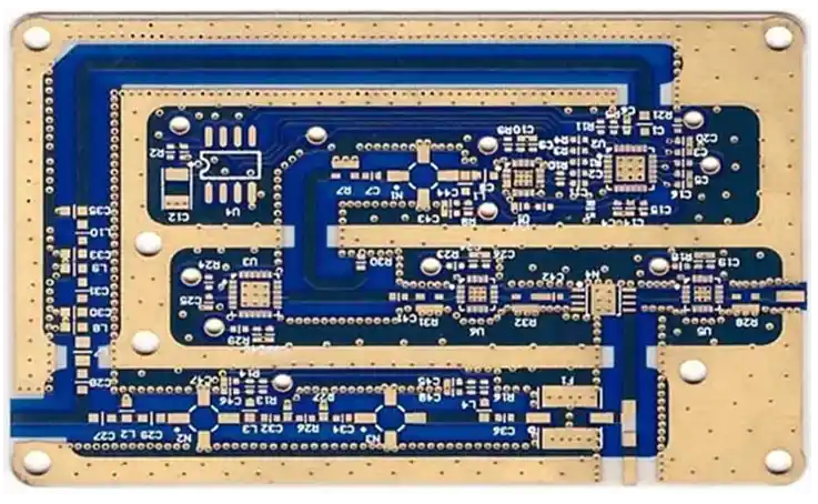
Material selection for high-frequency PCBs is a technical cornerstone, as these substrates dictate the electrical performance, environmental resilience, and cost-efficiency of the end product. Below is an in-depth exploration of the key material categories and their roles in high-frequency PCB production.
Low-Dielectric Constant (DK) Materials for High-Frequency PCBs
The dielectric constant (DK) is crucial for maintaining signal integrity at high frequencies. Materials with a low and stable DK reduce signal delay and power loss, making them indispensable in high-frequency designs.
Technical Overview-
1.PTFE (Teflon):
●Often preferred for applications above 10 GHz, PTFE exhibits a DK around 2.1 and a loss tangent (DF) as low as 0.001. However, its high thermal expansion requires careful handling during multilayer fabrication.
2.Rogers Laminates:
●Rogers 4350B: DK ~3.48, suitable for RF and microwave applications.
●Rogers RT/duroid 5880: DK ~2.2, optimal for high-frequency antennas due to minimal signal dispersion.
3.Other Notable Brands:
●Taconic RF-35: Offers similar low-loss properties to Rogers.
●Shengyi S7136: Cost-effective and well-suited for mid-frequency ranges.
Dielectric Properties-
| Material | DK (Frequency) | DF | Application |
| Rogers 4350B | 3.48 (10 GHz) | 0.0037 | Microwave circuits, amplifiers |
| Taconic TLY-5 | 2.17 (1 GHz) | 0.002 | Radars, satellite systems |
| PTFE-based Generic | ~2.1 | ~0.001 | High-speed data transmission |
High-frequency PCBs demand accuracy. Selecting the appropriate DK material ensures that RF energy remains precisely where it belongs—on the signal path.
Environmental Durability of High-Frequency PCB Materials
Environmental factors like moisture absorption and temperature stability can drastically affect PCB performance. High-frequency PCB materials must withstand these challenges while maintaining electrical and mechanical reliability.
Key Attributes to Assess-
1.Moisture Resistance:
●Arlon 25N: Absorption rate <0.1%, ideal for humid environments.
●Ventec VT-47: Designed for low moisture absorption with stable thermal performance.
2.Thermal Properties:
●Nelco N7000: Offers high Tg (>200°C), reducing warping in high-heat applications.
●Isola Astra MT77: Balances excellent thermal conductivity with low DK.
3.Durability in Field Applications:
●High-frequency boards in military radars or aerospace systems benefit from Arlon and Rogers materials due to their consistent performance under extreme fluctuations.
Environmental Properties Comparison-
| Material | Moisture Absorption (%) | Thermal Conductivity (W/m·K) | Tg (°C) |
| Arlon 25N | 0.05 | 0.25 | 190 |
| Nelco N7000 | 0.12 | 0.22 | 210 |
| Isola Astra MT77 | 0.10 | 0.30 | 200 |
Don’t let your design fail in the field. Choose materials engineered to handle moisture, heat, and unpredictable environments.
Cost vs. Performance in High-Frequency PCB Materials
While premium materials like Rogers or Teflon provide unparalleled performance, cost considerations often determine material selection for mass production. Here’s how to weigh the trade-offs:
Factors to Consider-
1.High-End Performance:
●Rogers RT/duroid: Exceptional for defense and aerospace due to low DK and DF, but costs $15–20 per sq. ft.
2.Budget-Friendly Options:
●Shengyi and Nanya: Offer competitive DK and DF values at a reduced price, suitable for consumer electronics.
3.Balancing Cost and Function:
●Mid-range laminates like Panasonic MEGTRON 6 provide stability for telecom infrastructure without the high expense of PTFE.
Cost vs. Performance Breakdown-
| Material | Cost ($/sq ft) | DK Stability | Primary Use |
| Rogers 4350B | 15–20 | Excellent | 5G, aerospace systems |
| Shengyi S7439 | 8–12 | Good | Consumer RF devices |
| Panasonic MEGTRON 6 | 10–15 | Very Good | Telecom infrastructure |
The right balance of cost and performance depends on your application’s demands. Why not optimize for the best of both worlds?
Critical Manufacturing Techniques for High-Frequency PCBs
High-frequency PCBs are precision-engineered to handle high-speed signals and complex applications in telecommunications, aerospace, and medical fields. Each manufacturing step demands meticulous attention to maintain signal integrity, reliability, and performance. This section explores critical techniques, offering detailed explanations, examples, and tables for clarity.
Precision Drilling and Via Technology in High-Frequency PCBs
When it comes to building solid signal pathways for high-frequency PCBs, drilling and via technologies are a game plan you can’t afford to miss. Methods like laser drilling, microvias, and buried or blind vias step up to the plate, helping minimize parasitic effects and boost signal flow. These advanced techniques allow for more compact designs and better control over signal integrity, ensuring that your high-frequency signals stay sharp and crisp. It’s all about crafting the right pathways to keep your signals on point and your design on track.
Key Considerations-
1.Laser Drilling: This technique allows for incredibly small hole diameters, as small as 0.1 mm, with a smooth surface finish, a must-have for high-frequency RF and microwave designs.
2.Microvias: Ensure short and direct signal paths, reducing losses and crosstalk in multi-layer designs.
3.Plating Quality: Ensures conductive layers are consistent, especially for high-frequency transitions.
Comparison of Drilling Techniques-
| Technique | Hole Size | Cost | Applications |
| Mechanical Drilling | >0.2 mm | Lower | Low-frequency PCBs, prototypes |
| Laser Drilling | <0.1 mm | Higher | RF, microwave, and high-frequency designs |
| CO2 Laser | Small, clean cuts | Moderate | Flex circuits and microvias |
●Example: A 6-layer RF communication PCB with microvias improved signal-to-noise ratio by 15%, meeting stringent telecom standards.
●Pro Tip: Always analyze the trade-offs between cost and performance when selecting a via structure.
Surface Finishes for High-Frequency PCB Reliability
Surface finishes directly influence solderability, oxidation resistance, and electrical performance in high-frequency environments. Selecting the appropriate finish ensures longevity and consistent signal propagation.
Common Surface Finishes-
1. ENIG (Electroless Nickel Immersion Gold): ENIG is one of the most widely used finishes for high-frequency PCBs due to its flat surface, excellent corrosion resistance, and strong mechanical properties. The nickel layer provides a barrier against copper diffusion, while the gold layer offers superior conductivity for RF signals.
2. HASL (Hot Air Solder Leveling): HASL applies a layer of molten solder over the PCB to protect the copper traces. While it is a cost-effective solution, it may not be ideal for high-frequency designs due to uneven surfaces and potential signal loss.
3. Lead-Free HASL: Lead-free HASL uses environmentally friendly solder and provides similar properties to traditional HASL. It offers better compatibility with RoHS regulations but still struggles with uneven surfaces.
4. Immersion Silver: Immersion Silver is often chosen for its excellent electrical conductivity, making it ideal for high-frequency PCBs where signal loss is a concern. It forms a thin, even layer over the copper traces.
5. Immersion Tin: This finish applies a layer of tin over the copper to prevent oxidation. It is cost-effective and provides a smooth surface but is prone to whisker growth, which can lead to short circuits.
6. ENEPIG (Electroless Nickel Electroless Palladium Immersion Gold): ENEPIG, also known as the “universal finish,” offers enhanced reliability with a palladium layer between nickel and gold. It ensures excellent wire bonding and protects against black pad issues.
7. OSP (Organic Solderability Preservative): OSP is a simple and environmentally friendly finish that protects copper surfaces during storage. While it provides a flat surface for soldering, it lacks the robustness needed for harsh environments.
8. Hard Gold and Flash Gold: Hard gold is an electroplated finish known for its abrasion resistance, while flash gold is a thinner version used to reduce costs. Both finishes provide excellent conductivity and durability.
Comparison Table of Surface Finishes-
| Finish Type | Flatness | Conductivity | Durability | Cost | Best Application |
| ENIG | Excellent | High | High | High | RF/Microwave, automotive |
| HASL | Poor | Moderate | High | Low | Prototypes, general use |
| Immersion Silver | Good | High | Moderate | Moderate | High-frequency applications |
| Immersion Tin | Good | Moderate | Low | Low | Consumer electronics |
| ENEPIG | Excellent | High | Very High | Very High | Aerospace, telecommunications |
| OSP | Excellent | Moderate | Low | Low | Low-complexity designs |
●Case Study: For a military-grade RF project, ENEPIG was selected to meet both high signal precision and environmental stress requirements.
●Pro Tip: Match your finish to the environmental conditions of the end application to avoid costly signal degradation.
Quality Assurance and Testing for High-Frequency PCBs
High-frequency PCBs are no easy feat to handle—they demand accuracy at every step, from design through to testing. PCB Manufacturers need to test everything, from how well the signals hold up to the thermal management setup, ensuring the board works seamlessly across its intended frequencies. Success is all about using top-tier tools and testing methods, ensuring the design not only looks good on paper but also holds up in real-world conditions. Let’s dive into the techniques and tools that ensure these designs pass the real-world test.
RF Signal Testing in High-Frequency PCB Manufacturing
In high-frequency PCB production, RF signal testing involves using sophisticated measurement equipment to verify the electrical characteristics of the circuit under real-world conditions. Vector Network Analyzers (VNAs) are the go-to for assessing key parameters like S-parameters, insertion loss, and return loss. These tests ensure the circuit maintains the desired frequency response without excessive attenuation or reflections that can degrade signal integrity.
When testing high-frequency PCBs, two key factors to focus on are return loss and insertion loss. Return loss shows whether the impedance between the trace and signal source is well-matched, which helps minimize signal reflection and loss. On the other hand, insertion loss measures the power loss as the signal travels through the PCB. Too much insertion loss can cause signal weakening and degradation, impacting the overall performance of the PCB. Ensuring these aspects are well-managed leads to reliable, high-quality signal transmission.
| Test Parameter | Test Equipment | Frequency Range | Typical Tolerance |
| Return Loss | VNA | 1 MHz to 40 GHz | ≥ 10 dB for proper signal transmission |
| Insertion Loss | VNA, Oscilloscope | 1 MHz to 40 GHz | < 0.5 dB per foot of trace |
| Crosstalk | Network Analyzer, VNA | 1 MHz to 40 GHz | ≤ -40 dB for isolated signal paths |
This kind of RF testing is not just about looking at numbers; it’s about making sure that the final PCB will hold up against real-world electromagnetic interference (EMI), which could easily compromise signal integrity if not tested and controlled.
Thermal Testing for High-Frequency PCB Durability
Thermal stress is a common cause of PCB failures, especially in high-frequency applications. As these PCBs operate at high speeds and frequencies, they generate heat, which can alter material properties, cause warping, and lead to component failure if not properly managed. Thermal cycling tests help simulate these extreme conditions and assess how well the PCB can handle temperature shifts without degrading.
Key aspects include thermal expansion matching between different layers of the PCB and the components, as mismatched thermal coefficients can lead to delamination. Thermal shock testing evaluates the PCB’s resilience to sudden temperature changes, ensuring that it can withstand conditions such as a sudden drop in temperature, which could cause cracks in solder joints or traces.
| Test Type | Equipment | Temperature Range | Test Objective |
| Thermal Cycling | Thermal Cycling Chamber | -55°C to +125°C | Stress test for material expansion and contraction |
| Thermal Shock | Thermal Shock Tester | -40°C to 150°C | Identify cracks or delamination caused by rapid shifts |
| Hot Spot Testing | IR Thermography | Ambient to 150°C | Detecting excessive localized heating during operation |
Testing for Impedance Control and Signal Integrity
Impedance control is one of the most challenging aspects of designing high-frequency PCBs. The PCB must ensure that each trace, via, and component is designed to match the system’s impedance and prevent reflections. If the impedance is inconsistent, it leads to signal integrity issues, including reflections, crosstalk, and noise. This can result in data corruption, loss of synchronization, and poor overall performance.
Time Domain Reflectometry (TDR) is commonly used to test impedance on PCBs. TDR sends a pulse through the trace and measures the reflected signal to calculate the impedance at different points along the PCB. This technique helps engineers detect mismatch issues, especially at high frequencies where signal behavior becomes non-linear. Bit Error Rate Testing (BERT) also helps evaluate the impact of signal loss and distortion on digital data transmission by measuring the rate of errors in the transmitted bits.
| Test Type | Test Equipment | Measurement Range | Purpose |
| Impedance Control | TDR, VNA | 1 MHz to 40 GHz | Checking consistency of impedance throughout traces |
| Signal Reflection | TDR, VNA | 1 MHz to 40 GHz | Identifying signal reflections due to impedance mismatch |
| Signal Integrity | BERT, Oscilloscope | DC to 40 GHz | Monitoring data transmission errors and signal quality |
Ensuring that the impedance is perfectly controlled in high-frequency designs is not just about maintaining signal integrity; it’s also about preventing costly operational failures in the long term.
Comparing High-Frequency PCBs with High-Speed PCBs
High-frequency PCBs and high-speed PCBs are often thought of as similar, but in reality, they are tailored for different types of signal transmission. The key differences between the two lie in their application, material requirements, and performance. Let’s break down how they differ and how their design considerations and real-world applications vary.
Frequency Range and Application Differences
The frequency range of a PCB determines its suitability for different applications, and this is a major distinction between high-frequency and high-speed designs. While high-speed PCBs focus on maintaining signal integrity in high-data-rate, digital environments, high-frequency PCBs are specialized for operating at GHz frequencies in RF and microwave applications.
1.High-Frequency PCB (1 GHz and above)-
●Typical Range: 1 GHz to 100 GHz (or more)
●Application: Used primarily in RF, microwave applications, wireless communications, military radar systems, 5G infrastructure, satellite communications, and aerospace.
●Signal Characteristics: At these frequencies, signal integrity is impacted more by the physical properties of the PCB material (e.g., dielectric constant, loss tangent) and electromagnetic interference (EMI).
2.High-Speed PCB (less than 1 GHz)-
●Typical Range: Up to 1 GHz (generally below)
●Application: Typically used in digital applications where signal transmission is high-speed but the frequency is not as high as GHz. Common applications include data transmission, computer circuits, memory cards, communication networks, and consumer electronics.
●Signal Characteristics: Focuses on achieving low-latency transmission and signal timing in high-data-rate environments.
Key takeaway: High-frequency PCBs excel in environments that demand stable performance at GHz frequencies, whereas high-speed PCBs are designed to manage the rapid flow of digital data, typically in lower frequency ranges (sub-1 GHz).
Design Challenges and Material Requirements
The design and material selection for both high-frequency and high-speed PCBs play a massive role in their performance, but there are critical differences based on the operating conditions.
1.High-Frequency PCBs-
●Low-Loss Dielectrics: These boards require materials that exhibit low dielectric loss to minimize signal attenuation. Materials like Rogers 4003C, Taconic TLY-5, and PTFE (Polytetrafluoroethylene) are commonly used for their low dielectric constant (Dk) and low dissipation factor (Df).
●Controlled Impedance: Impedance matching is critical for high-frequency applications. Transmission line theory must be applied to prevent reflection, ensuring the signal maintains its integrity.
●Thermal Considerations: High-frequency circuits often generate more heat due to high power densities. Thermal vias, heat sinks, and thermal pads are essential for managing this heat.
2.High-Speed PCBs-
●Signal Integrity and Crosstalk Prevention: While high-speed PCBs also require attention to impedance control, the primary focus is on maintaining digital signal integrity in a high-speed environment. Special routing techniques such as differential pairs and via stitching are employed to prevent crosstalk and noise.
●Material Flexibility: For high-speed PCBs, FR4 is often used due to its cost-effectiveness and reasonable electrical performance at lower frequencies. Polyimide materials are also used for their mechanical stability and flexibility.
Comparative Material Chart-
| Material Type | Application | Dielectric Constant (Dk) | Dissipation Factor (Df) | Max Frequency | Thermal Performance |
| Rogers 4003C | High-frequency PCBs | 3.48 | 0.0035 | 20 GHz+ | High |
| Taconic TLY-5 | High-frequency applications | 2.55 | 0.0040 | 10 GHz+ | Moderate |
| FR4 | High-speed digital PCBs | 4.4-5.2 | 0.02 | 500 MHz | Low |
| Polyimide | High-speed flex PCBs | 3.2-3.5 | 0.005 | 2 GHz | High |
Performance in Real-World Applications
In the real world, high-frequency PCBs and high-speed PCBs serve different industries, and understanding their performance in these fields can help in choosing the right type for a given application.
1.High-Frequency PCBs in RF and Microwave Applications-
●Applications: RF (Radio Frequency) and microwave systems (used in cellular networks, 5G technology, and aerospace radar systems) require stable, high-performance signal transmission over long distances and at very high frequencies.
●Example: A 5G base station needs high-frequency PCBs to handle millimeter-wave frequencies, which demand the use of low-loss materials and the ability to maintain signal fidelity over greater distances. Poor performance in these applications could lead to poor network speeds and coverage.
2.High-Speed PCBs in Data Transmission and Communication Networks-
●Applications: High-speed PCBs are used in systems that manage large volumes of data in applications like computers, network switches, and data centers. These boards prioritize fast digital signaling and low latency.
●Example: In a data center, high-speed PCBs are used in routers and switches to support high-volume data traffic. For instance, in high-frequency trading platforms, these boards help process large amounts of information quickly and efficiently.
Comparing the real-world performance of high-frequency and high-speed PCBs in common applications:
| Application | PCB Type | Frequency Range | Key Material Requirements | Performance Indicators |
| RF Communication | High-frequency PCB | 1 GHz – 100 GHz+ | Low-loss dielectrics (e.g., PTFE) | Signal Integrity, Low Attenuation |
| Microwave Communication | High-frequency PCB | 2 GHz – 40 GHz | Rogers, Taconic | Impedance Matching, Low Df |
| Data Transmission (Ethernet) | High-speed PCB | 500 MHz – 1 GHz | FR4, Polyimide | Low Latency, High-Speed Data Transfer |
| Data Center Infrastructure | High-speed PCB | 1 GHz – 10 GHz | FR4, Polyimide | High Data Throughput, Low Crosstalk |
Why Choose JarnisTech Circuit Board Manufacturer?
At JarnisTech, we understand the challenges of high-frequency PCB manufacturing. We focus on selecting premium materials and making smart design decisions to ensure optimal performance. With years of experience and expertise, we’ve established a solid reputation for delivering precise and reliable PCBs. Our solutions are built to meet the rigorous demands of high-speed applications, ensuring your projects perform at their best, every time.
1. Precision Engineering for Complex Designs
At JarnisTech, we’re not just about putting pieces together. We specialize in advanced techniques like depth-controlled drilling and precision back-drilling, also known as controlled-depth milling. These methods allow us to work with multi-layer, high-frequency designs with a focus on preserving signal integrity. By minimizing interference from vias and trace connections, we ensure your PCB works exactly how it’s meant to—no surprises. With our expertise, your designs will meet the performance standards needed for complex applications.
Our team leverages state-of-the-art technology, such as automated depth control during drilling, to minimize parasitic capacitance in high-frequency designs. This precision ensures that the drilled holes align perfectly with the signal path, preventing any interference that could affect the performance of the PCB. By focusing on every detail of the manufacturing process, we ensure that the final product performs consistently and efficiently across all high-frequency applications.
2. End-to-End Services: From Design to Assembly
Unlike many other PCB plates manufacturers, JarnisTech handles every stage of the PCB development process under one roof. From initial design consultation to material selection, prototype creation, and full-scale assembly, we manage the entire project lifecycle. This in-house capability not only streamlines the manufacturing process but also ensures superior quality control at each step.
When you partner with us, you’re not just getting a PCB; you’re gaining access to a dedicated team of engineers and technicians who work closely with you to refine your design and bring it to life. Whether it’s troubleshooting complex signal integrity issues or optimizing your layout for better performance, we’re with you every step of the way.
3. Why We’re Different: Expertise and Technology Combined
Our unique combination of expertise, technology, and a vast engineering team means we can confidently take on even the most complex projects. We are proficient in the intricacies of high-frequency PCB designs, ensuring that every component is carefully chosen, every trace is meticulously routed, and the final product meets your performance goals.
We also stay ahead of the curve by continuously integrating the latest advancements in PCB manufacturing, such as advanced material selection, precision via technologies, and customized surface finishes to ensure longevity and reliability. Whether it’s working with ceramic materials for better thermal management or high-speed laminates for faster data transmission, we have the tools and expertise to support a diverse range of applications.
4. Our Manufacturing Capabilities: Tailored to Your Needs
At JarnisTech, we don’t just follow industry standards; we set them. We have the experience to manage every aspect of PCB manufacturing, from basic single-layer boards to multi-layer complex high-frequency designs.
Our Manufacturing Capabilities:
| Specification | Capability |
| Layer Counts | 1-60 |
| Normal Lead Time | 5-6 days |
| Expedited Lead Time | 24-48 hours |
| Materials | FR4, High TG FR4, Halogen-Free CEM-3, Rogers HF, and more |
| Copper Thickness (Finished) | 1/3OZ-40OZ |
| Overall Board Thickness | 0.2-6 mm |
| Minimum Line/Track Width & Space | 2.5Mil/2.5Mil |
| Technology | Blind vias, impedance control, rigid-flex, and more |
| Other Technology | Gold finger, peelable mask, non-blind vias, and more |
| Solder Mask Color | Green, black, blue, white, red, yellow, matte, etc. |
| Legend/Silkscreen Color | White, yellow, black, etc. |
| Surface Treatment | HASL, Lead-Free HASL, Immersion Gold, OSP, Immersion Tin, etc. |
| Wrap and Twist | ≤0.7% |
| Qualifications | ISO 14001:2015, ISO 9001:2015, IATF 16949:2016 |
Global Reach with Local Expertise
Our reach extends across industries such as telecommunications, automotive, medical devices, aerospace, and more. With a focus on high-frequency RF circuits, we have helped clients across the world optimize their PCB designs for microwave frequencies, 5G applications, satellite communications, and other specialized applications requiring tight tolerance and robust performance.
By choosing JarnisTech, you’re not just getting a PCB manufacturer—you’re getting a partner with the experience, technology, and hands-on expertise to solve your most challenging PCB design and manufacturing needs.
FAQ& High Frequency PCB
What is the impact of temperature on High-Frequency PCB performance?
High temperatures can cause materials in high frequency PCBs to expand or contract, affecting signal integrity and impedance. Thermal management techniques and suitable materials are required to ensure performance consistency.
Can High-Frequency PCBs be used for both analog and digital signals?
High frequency PCBs can support both analog and digital signals, but careful design considerations are needed to maintain signal integrity, especially for high speed digital circuits.
How do High Frequency PCBs handle electromagnetic interference (EMI)?
High frequency PCBs often incorporate shielding, proper grounding, and careful layout design to minimize EMI and prevent interference from other electronic devices.
What is the significance of trace width in High Frequency PCB design?
Trace width directly affects impedance and signal integrity. For high frequency signals, precise control of trace width is required to minimize losses and reflection.
How does substrate material affect signal propagation speed in High Frequency PCBs?
The substrate material determines the signal’s propagation speed. Materials with low dielectric constants, like PTFE, are often used in high frequency PCBs to ensure faster signal transmission with minimal loss.
What are the challenges in manufacturing multi-layer High Frequency PCBs?
Multi-layer high frequency PCBs require precise alignment, impedance control, and specialized materials. The complexity increases with more layers, especially when managing signal integrity across multiple layers.
How does High Frequency PCB design differ for 5G and IoT applications?
5G requires higher frequency ranges, stricter impedance control, and low-loss materials compared to typical IoT designs, which may prioritize power efficiency and compact size.
What are the benefits of using flexible substrates in High Frequency PCB designs?
Flexible substrates allow for more compact, lighter designs that can bend without compromising signal integrity. These are ideal for wearable devices and applications requiring flexibility without sacrificing performance.

