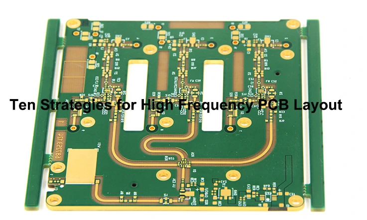
Designing and implementing high-frequency PCB layout necessitates cautious contemplation of various aspects to guarantee optimal performance and signal integrity. This post presents ten cardinal tactics for high-frequency PCB layouts. By following these guidelines, designers can effectively mitigate signal degradation, interference, and other challenges associated with high-frequency applications.
1.Multi-layer Board Wiring
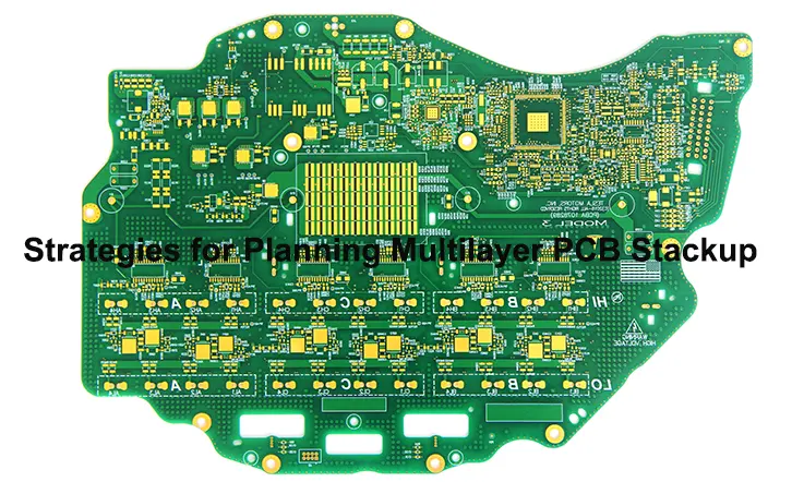
High-frequency circuitry typically stipulates significant integration coupled with dense wiring, achievable via the use of multi-layer PCB boards. These boards are instrumental in ensuring efficient wiring, and also provide a robust solution to diminish interference. During the PCB Layout stage, it is important to select a reasonable size for the printed board with a specific number of layers in order to fully utilize the intermediate layers for shielding purposes. By doing so, near grounding is improved, parasitic inductance is significantly reduced, signal transmission lengths are minimized, heightening the dependability of high-frequency circuits via crosstalk reduction and resolution of other signal-associated anomalies.
Based on available data, it has been observed that four-layer board exhibits a noise level 20dB lower than that of a double-panel board. Nonetheless, it’s imperative to recognize that augmenting the count of layers within a PCB invariably results in a more intricate fabrication process, and subsequently, elevated per-unit expenses. Therefore, it becomes crucial to carefully select the appropriate number of layers for the PCB layout. This selection should be accompanied by proper component layout planning and adherence to routing rules to successfully accomplish the design objectives.
The wiring process in multi-layer boards involves connecting various components and circuit elements through conductive traces, vias, and pads. Here are the key steps involved in multi-layer board wiring:
Component Placement:
The first step is to strategically place the components on the board to optimize signal flow, reduce signal coupling, and minimize parasitic effects. Proper placement of components secures shorter signal trajectories and promotes proficient routing.
Layer Assignment:
Depending on the complexity of the circuit and the desired signal integrity, the layers of the multi-layer board are assigned specific functions. These layers typically include signal layers, power and ground planes, and potential shielding layers for noise reduction.
Signal Routing:
After component placement, signal traces are routed to establish connections between components. High-frequency signals require careful consideration of trace lengths, impedance matching, and signal integrity. Differential pair routing may be necessary to minimize crosstalk and maintain signal integrity.
Power and Ground Planes:
Multi-layer boards often include dedicated power and ground planes, typically on internal layers. These planes provide a low impedance path for power distribution and serve as a reference for signal return currents, reducing noise and improving signal integrity.
Via Placement:
Vias are used to connect traces between different layers. Placing vias strategically helps to minimize signal distortion and reduces the overall impedance of the circuit. Care must be taken to avoid excessive via stubs that can introduce signal reflections.
Differential Pair Routing:
For high-speed and high-frequency circuits, differential pair routing is essential. This technique involves routing two traces that carry complementary signals in close proximity to maintain signal integrity and reduce electromagnetic interference.
Design Rule Check (DRC):
Once the routing is complete, a DRC is performed to ensure that the design meets the specified manufacturing and assembly guidelines. The DRC checks for any rule violations, such as clearance violations, minimum trace widths, and other design constraints.
Signal Integrity Analysis:
Signal integrity analysis tools can be employed to validate the design’s performance in terms of impedance matching, signal propagation delay, crosstalk, and reflections. This analysis helps identify any potential issues and allows for necessary adjustments to optimize signal integrity.
By following these steps, multi-layer board wiring can be effectively executed, resulting in improved integration, reduced interference, and enhanced signal performance for high-frequency circuits.
2.Minimizing Lead Bend for Enhanced High-Speed Electronic Device Performance
The preference generally leans towards reduced the quantity of lead bends connecting the pins of high-speed electronic devices. The reason behind this preference is that lead bends can introduce impedance variations, signal reflections and signal degradation. By reducing the number of bends, signal integrity can be better maintained, ensure the reliable and efficient high-speed signal transmission.
Excessive bends in the lead can cause the signal path to lengthen, resulting in delays and distortion. Additionally each bend adds capacitance and inductance which may impact signal quality and raise concerns, about reflections and crosstalk.
To achieve optimal signal integrity, to keep the lead length and routing as straight as possible, minimizing unnecessary bends. However, it is important to strike a balance between lead length and other design considerations. Such as, component placement, space constraints and manufacturability. Careful planning and adherence to design guidelines can help achieve a balance between minimizing lead bends and meeting other design requirements while maintaining signal integrity in high-speed electronic devices.
3.Optimizing High-Frequency Circuit Device Performance with Shorter Lead Length
The radiant intensity of a signal is directly proportional to the length of the trace of the signal line, consequently amplifying the chance of coupling with adjacent components on longer high-frequency signal leads. It is hence essential to be mindful in maintaining the signal lines pertinent to crucial data – such as signal clock, crystal, DDR, and high-frequency lines like LVDS, USB, HDMI – at the shortest length attainable.
By minimizing the length of these signal lines, the risk of coupling or interference with neighboring components is reduced. This is particularly important for high-frequency signals, as longer leads can result in increased electromagnetic radiation and susceptibility to external noise sources.
Shortening the signal lines helps to maintain signal integrity, minimize signal degradation, and reduce the potential for signal reflections and crosstalk. By ensuring these high-frequency signal lines are kept to their minimal length feasible, the comprehensive performance and dependability of the circuit can be augmented, assuring precise and steady data transmission.
4.Enhancing High-Frequency Circuit Device Performance by Reducing Interleaving between Lead Layers
The principle of “minimizing the number of layer transitions for leads” suggests that it is advantageous to minimize the usage of vias in the interconnection process of components. This is because each via introduces distributed capacitance, typically around 0.5pF, which can have a notable impact on signal performance. By reducing the number of vias, the speed of signal transmission can be significantly increased, and the likelihood of data errors can be reduced.
Vias, while necessary for vertical interconnections between different layers of a multi-layer PCB, can introduce parasitic effects such as capacitance, inductance, and signal reflections. These effects can degrade signal integrity, increase signal propagation delay, and potentially introduce noise or interference.
Decreasing the quantity of vias results in less overall capacitance and inductance in the signal route, which leads to ameliorated signal quality and boosted transmission velocities. Additionally, lessening the counts of vias smooths the routing and interlinking process, thereby cumulating the manufacturability and possibly cutting down the associated costs.
Nonetheless, a delicate equilibrium should be struck between minimizing vias and meeting other crucial design requirement, such as the arrangement of the components and board density. Careful consideration should be given to the specific circuit requirements and signal integrity analysis to determine the optimal number and placement of vias for a given design.
5.Mitigating Crosstalk in High-Frequency PCB Designs: Managing Parallel Signal Lines
In high-frequency circuit wiring,, effectively dealing with the matter of ‘crosstalk’ – a byproduct of parallel signal lines, becomes imperative. Crosstalk refers to the undesired coupling phenomenon between signal lines that are not directly connected. When High-frequency signals travel via transmission lines shaped as electromagnetic waves, hence signal lines inherently perform as antennas, disseminating electromagnetic energy. This mutual coupling of electromagnetic fields leads to the generation of undesired noise signals, known as crosstalk, between the signals.
Diverse factors, encompassing PCB layer parameters, distance between signal lines, electrical properties of drivers and receivers, along with signal line termination, have the propensity to affect cross-talk. Consequently, to mitigate cross-talk in high-frequency signal wiring, the following considerations should be taken into account:
●Inserting a ground or ground plane between signal lines with significant crosstalk can provide isolation and reduce crosstalk, provided that the available wiring space permits it.
●When parallel distribution of signal lines is unavoidable in the presence of time-varying electromagnetic fields, placing a large ground area on the opposite side of the parallel signal line can significantly reduce interference.
●Within the limit of wiring space, increasing the spacing between adjacent signal lines and minimizing the parallel length of the signal lines is recommended. It is also advisable to ensure that clock lines are perpendicular to key signal lines rather than running in parallel.
●Should it be unavoidable to have parallel traces on the same layer, it becomes critical to ascertain that the traces on layers adjacent to each other exhibit a perpendicular orientation.
●In digital circuits, clock signals typically exhibit fast edge changes, making them more susceptible to external crosstalk. To mitigate this, the clock line should be surrounded by ground lines and incorporate additional ground holes to reduce distributed capacitance and minimize crosstalk.
●For high-frequency clock signals, utilizing low-voltage differential signaling and employing ground shielding are recommended. Attention should be given to package integrity to ensure effective signal transmission.
●It is important not to leave unused input terminals floating. Instead, they should be grounded or connected to the power supply (which is also considered ground in high-frequency signal loops).
Leaving a line floating can act as an emitting antenna, while grounding it suppresses emissions. This method has proven effective in reducing crosstalk immediately in certain cases.
6.Enhancing High-Frequency Decoupling: Increasing Power Supply Capacitance at IC Blocks
To lessen high frequency harmonics and disruption on the power supply terminals of integrated circuit segments, a widely accepted method includes the incorporation of a high-frequency decoupling capacitor. This capacitor functions to efficaciously quash high frequency disturbances present on the power supply conduits.
By integrating a high frequency decoupling capacitor to the power supply terminal of each integrated circuit segment, the capacitor initiates low impedance route for high frequency currents. It contributes to the stabilization of the power supply voltage and curtails voltage fluctuations instigated by high-frequency harmonics. Consequently, this diminishes the possibilities for interference and guarantees the reliable operation of the integrated circuit.
The high-frequency decoupling capacitor functions by contributing an alternate current route for high-frequency components of the load current. It acts as a bank of charge, promptly reacting to sudden alterations in current demand during high-frequency toggling. By this action, it helps to conserve a stable and pure power supply voltage for the integrated circuit, averting the dispersal of high-frequency noise throughout the electronic circuit.
The determination of fitting high frequency decoupling capacitor should take into account factors including capacitance value, equivalent series resistance (ESR), and equivalent series inductance (ESL). These traits influence the efficacy of the decoupling capacitor in dampening high frequency noise and reducing voltage fluctuations on the power supply terminals.
7.Isolating Grounds: High Frequency Digital Signal Ground and Analog Signal Ground Separation
When integrating analog ground lines with digital ground lines onto a common ground line, addressing the possible complications brought about by high-frequency noise becomes critical. To alleviate these complications, implementing high-frequency ferrite beads for connection or opting for direct isolation is suggested. Moreover, choosing an appropriate location for a single-point interconnection is advisable.
The ground potential of high frequency digital signal ground lines often exhibits inconsistency, resulting in a voltage difference between them. However, the ground of high frequency digital signals often include numerous harmonic constituents of high-frequency signals. When there is a direct connection between the digital signal ground and the analog signal ground, the harmonics of the high frequency signal can disrupt the analog signal via ground coupling.
To mitigate such disturbances, isolating the ground of the high frequency digital signal from that of the analog signal is commonly suggested. This can be accomplished by leveraging a single-point interconnection at a strategically chosen location or by incorporating the use of high-frequency ferrite beads for the purpose of interconnection.
Isolation of the grounds can substantially diminish the spread of high frequency harmonics and noise between the digital and analog signals. As practical filters, the high-frequency ferrite beads assist in reducing high frequency noise and obstructing its propagation through the ground links. This approach of isolation helps uphold the authenticity of the analog signal and lower the likelihood of disruption as a result of high-frequency harmonics.
Conscious thought should be placed on the placement and routing of the high-frequency ferrite beads or the choosing of an apt location for single-point interconnection. This strategy ensures maximum isolation and constricts the influence of high-frequency noise on the analog signals, allowing for reliable and accurate analog signal processing.
8.Avoid Loops Formed by Traces
Minimization of loop formation in high-frequency signal traces is an essential practice wherever practicable. In scenarios where the creation of a loop is inevitable, attempts should be made to confine the loop area to the smallest possible size. This practice plays a fundamental role in preserving signal integrity and lowering the chances for adverse implications.
Forming loops in high-frequency signal traces can introduce various issues, including increased inductance, stray capacitance, and electromagnetic interference. These factors can adversely impact signal quality, introduce signal degradation, and lead to crosstalk or noise coupling.
By minimizing the formation of loops, the overall loop area is reduced, which helps to mitigate the aforementioned issues. A smaller loop area results in reduced inductance and stray capacitance, minimizing the potential for signal distortion and interference. It also helps to limit the loop’s susceptibility to external electromagnetic fields.
In circumstances where the creation of a loop is inescapable, it’s still prudent to restrain the loop area to the smallest extent achievable. This can be accomplished through careful placement and routing of the signal traces, assuring that the loop is restricted within a confined scope. By adapting such measures, the harmful impacts correlated with expansive loop areas can be alleviated.
In addition, it’s critical to acknowledge that loop formation should be reduced in all classifications of high-frequency signal traces. This includes clock lines, data lines, and power delivery lines. The consistent observance of the principle of minimizing loops or ensuring loop areas are compact contributes to the total signal integrity and diminishes the potential for interference or signal degradation.
9.Ensuring Optimal Signal Impedance Matching
During signal transmission, mismatches in impedance can lead to signal reflections in the transmission channel. These reflections can cause the synthesized signal to overshoot and result in signal fluctuations around the logic threshold.
Maintaining a continuous ground plane offers several advantages. It furnishes a low impedance reference for signal return courses, reduces the effect of electromagnetic interference (EMI), and supports to sustain a stable ground potential throughout the circuit. Consequently, it guarantees accurate signal conveyance, mitigates noise coupling, and boosts the entire system’s performance.
Additionally, it is important to avoid abrupt changes or corners in the transmission line on the PCB. Maintaining continuous impedance at each point of the transmission line is essential to prevent reflections between different segments of the transmission line.
To achieve these goals, certain wiring rules should be followed when performing high-speed PCB routing for specific applications:
USB Wiring Rules:
USB signal differential routing requires a line width of 10 mils, a line spacing of 6 mils, and a separation of 6 mils between the ground and signal lines.
HDMI Cabling Rules:
HDMI signal differential routing necessitates a linewidth of 10 mils, a line spacing of 6 mils, and a spacing of at least 20 mils between each pair of HDMI differential signal pairs.
LVDS Routing Rules:
LVDS signal differential traces should have a linewidth of 7 mils and a line pitch of 6 mils. These guidelines aim to control the impedance of the HDMI differential signal pairs within a range of 100±15 ohms.
DDR Routing Rules:
For DDR1 routing, it is advisable to minimize signal paths passing through holes, maintain equal line widths, and ensure equidistant spacing between lines. Following the 2W principle helps to reduce crosstalk between signals. For high-speed devices using DDR2 and above, where high-frequency data transmission is involved, it is essential to maintain equal line lengths to ensure impedance matching of the signals.
10.Preserving Signal Transmission Integrity
To ensure the integrity of signal transmission and prevent the occurrence of “ground bounce” resulting from ground segmentation, it is essential to implement proper design practices.
Ground bounce is an undesirable variance in the ground potential instigated by the segmentation of the ground plane. This occurrence could result in a multitude of issues like signal integrity complications, amplified noise levels and potential dysfunctions in the circuitry.
To address this, it is crucial to maintain a continuous and unsegmented ground plane whenever possible. By avoiding unnecessary ground segmentation, designers can minimize the potential for ground bounce and its associated detrimental effects.
Maintaining a continuous ground plane offers several advantages. It provides a low impedance reference for signal return paths, reduces the impact of electromagnetic interference (EMI), and helps to maintain stable ground potential throughout the circuit. This, in turn, ensures proper signal transmission, minimizes noise coupling, and enhances overall system performance.
In situations where ground segmentation is unavoidable due to design constraints, it is important to implement appropriate measures to mitigate ground bounce. This can be achieved by employing techniques such as the use of ground stitching vias, which help to establish connections between different ground segments and maintain a more uniform ground potential.
Moreover, it is vital to meticulously observe the placement and routing of delicate signals concerning ground segmentation. Signal traces should be orchestrated in a manner that they possess a return course on the same ground segment, thereby diminishing the probability of encountering signal integrity problems aroused by ground bounce.
Final Thought
Designing high-frequency PCB layouts demands a systematic and meticulous approach. By implementing the ten essential strategies outlined in this article, designers can optimize signal integrity, minimize electromagnetic interference, and ensure reliable high-frequency performance. From proper component placement and optimized trace routing to impedance matching and ground plane considerations, each strategy plays a crucial role in achieving successful high-frequency PCB designs.
By complying with these guidelines and capitalizing on suitable simulation tools along with best practices, designers are able to exploit the maximum capabilities of high-frequency circuitry, thus allowing for sturdy and proficient operation. Adopting these strategies will authorize designers to confront the intricacies involved in high-frequency PCB layouts and supply innovative solutions in a diverse span of applications.

