
The landscape of mobile phone PCB design and manufacturing has grown to be one of the most technically challenging yet rewarding aspects of the electronics world. Whether it’s creating HDI designs for compact smartphones or innovating with flexible PCBs, every aspect of mobile PCB technology demands both a deep technical understanding and an agile approach to problem-solving. Let’s break down the current best practices, design considerations, and manufacturing innovations that are reshaping this field.
Types of Mobile Phone PCBs and Structural Considerations
When diving into the design of mobile phone PCBs, one must consider a range of PCB types that each serve different applications, depending on device needs. Let’s break down the key types: Single-layer, Double-layer, Multilayer, and more advanced designs like HDI and Rigid-Flex boards. Understanding the structural requirements is key to crafting the perfect mobile PCB.
Single-layer, Double-layer, and Multilayer Phone PCB Applications
Single-layer PCBs are the simplest and most cost-effective option, but they have limitations. Commonly used in basic mobile devices or peripheral accessories, they only provide one conductive layer, making them less efficient for handling multiple high-speed components.
Double-layer PCBs, on the other hand, are widely used in smartphones. They offer more space for routing signals and providing power distribution across two conductive layers. This design choice enhances the ability to integrate more components without sacrificing performance.
Multilayer PCBs take the cake for performance. With three or more layers, these PCBs enable engineers to pack even more components into the device. This type of PCB is perfect for advanced smartphones with numerous high-speed processors, sensors, and wireless communication modules. For example, Apple’s latest iPhone series relies on multilayer PCBs for both efficiency and performance, making it possible to handle 5G speeds, large batteries, and multiple cameras without overheating or sacrificing space.
Here’s a handy comparison:
| PCB Type | Advantages | Disadvantages | Common Use |
| Single-layer | Low cost, simple design | Limited space, fewer components | Basic mobile accessories |
| Double-layer | Better space utilization, good for medium complexity | Still space-constrained compared to multilayer | Mid-range smartphones |
| Multilayer | High performance, compact, can handle complex circuits | More expensive, complex to manufacture | High-end smartphones (e.g., iPhone, Galaxy) |
HDI (High-Density Interconnect) Mobile Phone PCB Innovations
As smartphones get thinner and more powerful, High-Density Interconnect (HDI) PCBs have taken center stage. HDI PCBs enable the packing of even more components in smaller spaces. They employ microvias and stacked vias, allowing engineers to place components closer together without sacrificing performance. These boards are particularly useful for devices that need high-speed data transfer, such as 5G phones or augmented reality (AR) headsets.
A great example? The Samsung Galaxy S21 relies on HDI technology to keep its small form factor, while integrating powerful processors, high-resolution cameras, and extensive connectivity options. Engineers working with HDI boards must be precise, as the technology involves high levels of density that require expert PCB layout.
HDI is not just about density but about managing the heat and electrical noise that come with more compact designs. When engineers go the HDI route, they have to ensure signal integrity and minimize interference, while optimizing thermal performance.
Flexible and Rigid-Flex Mobile Phone PCBs
While rigid PCBs are the go-to for traditional smartphones, flexible and rigid-flex PCBs are becoming more popular for modern devices that require adaptability and more complex designs.
Flexible PCBs offer the ability to bend and conform to unique shapes, making them ideal for foldable phones and wearables like smartwatches. Think of how the Samsung Galaxy Z Fold integrates flexible PCBs to achieve its foldable form factor. Flexible PCBs allow for more freedom in device design and can reduce weight, especially in compact devices that demand space-saving solutions.
Rigid-flex PCBs, as the name suggests, combine the benefits of both rigid and flexible PCBs, and they’re particularly used when designs need both flexibility and durability. These PCBs can be found in applications like wireless charging modules or embedded systems, where the PCB needs to remain rigid in certain areas but flexible in others to meet mechanical constraints.
| PCB Type | Applications | Benefits | Challenges |
| Flexible PCBs | Foldable screens, wearables, compact designs | Compact, lightweight, adaptable | Higher manufacturing costs |
| Rigid-Flex PCBs | Wearables, wireless charging, internal circuits | Combines the best of rigid and flexible | Complex design and assembly |
When considering which type of PCB to use, it’s all about matching the design requirements with the form factor and the performance needs of the device.
Key Components in Mobile Phone PCB Layout
Designing a mobile phone PCB requires a thorough understanding of various components that influence the overall performance and efficiency of the device. Let’s break down the key elements of a mobile PCB layout, focusing on how microprocessors, power management, and signal processing are integrated into modern smartphones.
Microprocessors and Battery Connections on Phone PCBs
Microprocessors are at the heart of every smartphone, and their placement on the PCB is a careful art. The microprocessor controls everything from the operating system to the application layer, making it a primary focus in PCB design.
In mobile phone PCB layouts, the microprocessor must be placed in a location that minimizes heat buildup and maximizes signal routing efficiency. Engineers also pay special attention to the battery connections since the power distribution must be optimized to ensure the device lasts longer on a single charge. Poor power management and inefficient connections can lead to shorter battery life and overheating.
Let’s use the Qualcomm Snapdragon 888 as an example. This microprocessor, used in many high-end Android phones, features high processing speeds and energy efficiency. Its positioning on the PCB layout directly impacts the signal integrity and thermal management of the device. Placing it too close to other heat-sensitive components can result in performance throttling, which no smartphone user wants.
Power Management in Mobile Phone PCB Design
Power management is a big deal in mobile phone PCB design. With modern smartphones demanding power like never before, the system needs to keep up without skipping a beat. Components like voltage regulators, capacitors, and power ICs need to be placed and routed with precision to ensure power flows smoothly to every part of the device, from the screen all the way down to the processor. Think of it as making sure every part of the car gets fuel to keep the engine running at full speed.
Power management systems in mobile PCBs are responsible for efficiently distributing power from the battery to various components without causing excessive heat generation or reducing performance. Effective thermal dissipation techniques such as heat sinks and thermal vias are crucial in keeping the power system under control.
Consider how the Apple iPhone utilizes power management ICs (PMICs) for dynamic voltage scaling (DVS), which adjusts power consumption based on the phone’s processing load. These components help maintain the balance between performance and power consumption. If you’re working on designing power-efficient boards, keeping an eye on power distribution pathways and reducing unnecessary voltage drops should be a priority.
Power Management Components Comparison-
| Power Management Component | Function | Typical Use in Mobile PCBs | Impact on Design |
| Power ICs (PMICs) | Manages voltage levels and power distribution | Handling power for processors, displays, and peripherals | Ensures smooth power flow, reduces power consumption |
| Voltage Regulators | Converts input voltage to a usable level | Regulating voltage to specific components | Crucial in ensuring correct voltage for optimal performance |
| Capacitors | Stores and releases electrical energy | Filtering power supply, stabilizing voltage | Helps smooth out power fluctuations and minimizes noise |
| Inductors | Stores energy in a magnetic field | Power supply filters and smoothing | Essential for stable power output and noise reduction |
| Thermal Vias | Channels heat away from sensitive components | Placed near high-power ICs like processors | Reduces overheating and improves thermal efficiency |
Signal Processing and RF Design in Phone PCBs
Signal processing and RF (Radio Frequency) design are fundamental in modern smartphones, enabling everything from Wi-Fi and Bluetooth connectivity to cellular communication. In the PCB layout, signal routing for RF components must be precise to avoid interference and signal degradation.
RF components like antennas and radio chips are strategically placed on the PCB to ensure the best reception and transmission. Engineers use specialized techniques like differential signaling and ground planes to shield and isolate signals for optimal performance. PCB layers must be designed to support high-frequency signals while minimizing electromagnetic interference (EMI).
A great example of RF engineering can be seen in 5G mobile phones, which use multiple antennas to handle high-frequency 5G signals. Engineers must account for both the antenna’s size and placement, ensuring they can maintain a stable connection while minimizing space usage.
When designing for RF, picking the right materials is just as crucial as the layout. High-performance RF designs often use PTFE (Polytetrafluoroethylene) and ceramic-based PCBs because of their low dielectric loss, which ensures a solid signal transmission. Plus, making sure the signal routing paths match impedance is key to prevent reflections and signal degradation. It’s like making sure your road is smooth and clear—no bumps or detours to slow down the signal.
RF Components Comparison-
| RF Component | Function | Impact on Mobile PCB Layout | Considerations in Design |
| Antenna | Transmits and receives radio signals | Placement and routing impact signal quality | Must be carefully positioned to avoid interference and signal loss |
| RFIC (Radio Frequency IC) | Handles RF signal processing | Must be placed in a way that minimizes EMI | Needs careful routing to avoid noise and power loss |
| Microstrip Lines | Conducts RF signals with minimal loss | Affects signal integrity, especially in 5G and Wi-Fi bands | Impedance matching is critical to prevent signal reflection |
| Filters and Switches | Filters out unwanted signals and frequencies | Protects system from noise and interference | Needs to be placed in areas where they won’t interfere with signal routing |
Essential Design Principles for High-Performance Phone PCBs
Designing a high-performance mobile phone PCB requires a fine balance of several key elements. From efficient component placement to precise signal routing, every detail can affect the final performance and durability of the device. Let’s break down the core principles behind creating robust mobile PCBs that keep up with modern demands.
Optimizing Component Density in Mobile Phone PCBs
As mobile devices get smaller and the need for faster processing ramps up, packing more components into a smaller space without sacrificing performance or durability becomes a top priority. Getting this balance right means bringing together cutting-edge design strategies and high-end manufacturing methods. It’s like fitting a high-powered engine into a compact car: making the most of every inch while keeping things running like a well-oiled machine. This requires precision and expertise to ensure everything fits and functions seamlessly.
Component density is influenced by various factors such as:
1.Miniaturization of Components: To boost performance while keeping things compact, smaller components like chipsets and capacitors are a game plan for increasing PCB density. With advancements in HDI (High-Density Interconnect) technology, parts can now be packed tighter together, all without stepping on each other’s toes. This innovation allows for more powerful devices in smaller footprints, so designers can push boundaries without running into interference issues. It’s like finding a way to fit more gear in a suitcase without it all getting jumbled up.
2.Layered Design: Multi-layer PCBs are commonly used in mobile phone designs to allow for higher component density. By creating stacked layers, more components can be placed in a smaller footprint while maintaining clean signal paths.
For example, Apple’s iPhone has incorporated advanced multi-layer PCBs to fit more powerful hardware into increasingly compact designs. This not only saves space but also ensures that components are adequately shielded from noise, which is a big deal when managing high-speed signals.
Let’s look at how HDI can benefit PCB density:
| Component Type | Size | Impact on Design | Design Optimization |
| Microprocessors | Small, high-performance | Central to design, need precise routing | Optimized placement to reduce heat and noise |
| Capacitors | Tiny, multi-layered | Used for power filtering, crucial in high-density PCBs | Placement must minimize parasitic inductance |
| Resistors | Small and flat | Key in signal processing and power regulation | Ensure spacing to avoid signal distortion |
The challenge is keeping the signal integrity intact, ensuring that power distribution remains even, and ensuring the PCB doesn’t get too hot due to component density.
Managing Signal Integrity on Dense Phone PCB Layouts
Keeping signal integrity in check is no small feat when it comes to mobile PCBs. With more and more tech packed into tighter spaces, even a little noise can throw off your whole setup, causing glitches and slowdowns. It’s like trying to hear your favorite song at a noisy concert—if the signal isn’t clean, you’ll get nothing but static. To avoid that, designers need to ensure every signal stays crisp and clear, or things could start to get messy fast.
In densely packed PCBs, the following methods are key for maintaining signal quality:
1.Grounding and Shielding: Proper grounding layers and shielding techniques ensure that high-frequency signals don’t interfere with each other. A common solution is the power-ground plane where a continuous, low-resistance path is provided for both power and ground signals.
2.Impedance Matching: Ensuring that signal traces are matched with the impedance of the components they connect to reduces reflection and loss of signal. Precision in trace width and materials used (like Teflon or PTFE) can significantly improve performance.
3.Differential Signaling: In high-speed circuits, differential signaling uses two opposite signals to keep transmission steady and reduce noise. This is especially true for fast technologies like 5G and Wi-Fi 6, where smooth, uninterrupted communication is a must. By sending signals in pairs, it minimizes interference, ensuring the data flows cleanly, even when speeds go through the roof. This method keeps devices firing on all cylinders, providing reliable, high-quality connectivity when you need it most.
Signal Integrity Example in High-Density Layouts-
| Signal Issue | Solution | Best Practice |
| Signal Reflection | Use controlled impedance traces | Match trace width and material for impedance |
| Electromagnetic Interference (EMI) | Use shielding and guard bands | Apply ground planes to reduce EMI |
| Cross-talk Between Traces | Increase trace spacing, optimize routing angles | Isolate critical signal traces from noisy ones |
An excellent example of managing signal integrity is Qualcomm’s Snapdragon processors, which have integrated power-efficient signal processing, ensuring that despite the compact layout, performance remains stable and high.
Material Choices for Durable Mobile Phone PCBs
The material selection for mobile phone PCBs significantly impacts the device’s durability, performance, and thermal stability. As phones become more advanced, materials used for the PCBs must be robust, heat-resistant, and electrically conductive.
Here are the most common materials used:
●FR4 (Flame Retardant 4): This is the most widely used material for standard mobile phone PCBs. It’s cost-effective, offers a good balance of electrical properties, and can be used for most basic designs.
●Polyimide: Ideal for flexible PCBs and applications where the PCB needs to bend or flex without cracking. It’s often used in foldable phones and compact designs where flexibility is needed.
●PTFE (Teflon): A preferred material in high-frequency applications like RF and 5G. Its low dielectric constant and minimal signal loss make it a go-to choice for high-performance mobile PCBs.
●Ceramic-based PCBs: Ceramic is widely used in high-power and high-heat scenarios. These PCBs are great for power management ICs and areas where heat dissipation is paramount.
Material Comparison for Mobile Phone PCBs-
| Material | Properties | Ideal Use Cases | Design Benefit |
| FR4 | Flame retardant, good electrical insulation | Most mobile phone PCBs | Cost-effective, reliable for standard designs |
| Polyimide | Flexible, heat-resistant, electrically stable | Flexible and foldable phones | Enables flexible and rugged designs |
| PTFE (Teflon) | Low dielectric constant, minimal loss at high frequencies | High-frequency, RF, and 5G applications | Enhances signal integrity in RF communication |
| Ceramic | High thermal conductivity, durable | High-performance, power-intensive components | Efficient thermal management and high reliability |
The use of these materials is a testament to the evolving landscape of mobile PCB design. By choosing the right material, we can not only enhance the performance but also prolong the lifespan of the mobile device.
Advanced Manufacturing Techniques for Mobile Phone PCBs
As the mobile industry moves toward more compact, more powerful devices, the demand for advanced mobile phone PCBs is rising. The manufacturing process is no longer just about laying down copper traces. Modern mobile phone PCBs require cutting-edge technologies and precision to meet the high expectations for performance and durability. In this section, we’ll explore some of the most advanced manufacturing techniques driving the industry forward.
HDI and Microvia Technology in Mobile Phone PCB Production
High-Density Interconnect (HDI) and microvia technology are reshaping the way mobile phone PCBs are designed and produced. These technologies enable manufacturers to achieve higher component density while maintaining excellent electrical performance. HDI technology, which uses finer lines and smaller holes than conventional PCBs, is a go-to solution for modern mobile devices that need to pack more power into smaller spaces.
Microvia technology, a subset of HDI, involves drilling extremely small vias—sometimes as small as 0.1mm in diameter—into the PCB to create connections between layers. This process allows for the miniaturization of components without sacrificing signal integrity or causing interference. The result? A mobile phone PCB that is not only compact but also efficient and high-performing.
Benefits of HDI and Microvia in Mobile Phone PCBs-
| Technique | Benefits | Impact on Design |
| HDI Technology | Enables smaller trace widths, higher routing density | Allows for compact designs with more power, like 5G antennas |
| Microvia | Allows for dense, multi-layer designs | Reduces the space required for via holes, optimizing component placement |
For example, Samsung’s premium Galaxy models rely on HDI-based PCBs to meet the demand for more compact components, ensuring performance isn’t sacrificed. The use of microvias allows for denser designs, optimizing space, and improving signal integrity. This design not only fits more components into smaller spaces but also supports high-speed data transfers like those required for 5G, making the phone’s connectivity sharp and smooth as butter. The result is a reliable, fast device that performs without a hitch, even under heavy use.
Manufacturing Processes for Flexible Phone PCBs
Flexible PCBs are becoming an essential part of mobile phone PCB design, especially for devices like foldable phones and wearables. These flexible circuits allow for bending and folding without damaging the electronic components, providing a whole new level of design freedom for manufacturers.
The manufacturing process for flexible PCBs involves the use of specialized materials like polyimide or PET (polyethylene terephthalate), which can withstand bending without cracking. The key to producing high-quality flexible PCBs lies in precise etching and lamination, which ensures that the flexible material can handle stress without losing signal integrity.
For example, Motorola’s Razr smartphone incorporates flexible PCBs to enable its foldable screen, showcasing how flexibility doesn’t have to come at the cost of performance.
Flexible PCB Production Process-
| Step | Description | Example Application |
| Material Selection | Choosing polyimide or PET for flexibility and durability | Used in foldable phones and wearables |
| Etching and Lamination | Creating the circuit layers and bonding them to the flexible material | Essential for maintaining electrical connections in flexible designs |
| Testing | Ensuring flexibility, durability, and signal performance | Foldable phones like the Motorola Razr rely on these tests for durability |
The success of flexible PCBs in the mobile industry shows how far technology has come, where bending and folding have moved from gimmicks to standard features in high-performance smartphones.
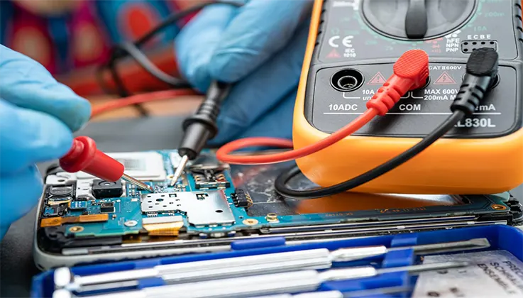
Quality Control for Reliable Mobile Phone PCB Production
A reliable mobile phone PCB depends heavily on stringent quality control (QC) processes throughout the manufacturing cycle. With the increasing complexity of mobile PCBs, quality control has become more sophisticated, ensuring that each board meets high standards for signal integrity, thermal performance, and durability.
Advanced QC procedures typically include automated optical inspection (AOI), X-ray inspection for hidden layer verification, and electrical testing to ensure that all connections are properly made and no shorts or breaks exist in the PCB.
In the world of mobile phone manufacturing, a single defect in a PCB can render an entire device unusable, leading to significant financial losses. That’s why manufacturers like Apple and Huawei utilize top-notch quality control systems to ensure every board is up to spec before it’s sent out for assembly.
QC Methods in PCB Manufacturing-
| Method | Purpose | Why It’s Important |
| Automated Optical Inspection (AOI) | Detects surface defects, missing components, or incorrect placement | Helps catch issues early, reducing rework costs |
| X-ray Inspection | Verifies internal layers and solder joints | Essential for inspecting multi-layer boards |
| Electrical Testing | Ensures all traces are properly connected and working | Prevents faulty PCBs from reaching the assembly line |
PCB Manufacturers use these techniques to catch even the most minute defects, ensuring that mobile phone PCBs meet strict industry standards for both reliability and performance.
Assembly Best Practices for Phone PCBs in Mobile Devices
When assembling mobile phone PCBs, it’s crucial to pay attention to precision in every step. From placing components with accuracy to ensuring reliable connections between boards, every move counts. The right assembly process ensures that your device works as expected in any scenario, providing stable performance. This section will explore best practices for PCB assembly, like precise component placement, maintaining solid connections, and meeting inspection standards. Getting these details right guarantees that your mobile device works flawlessly, with no room for mistakes.
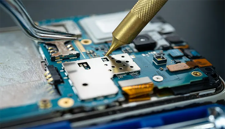
High-Precision Placement and Soldering on Mobile Phone PCBs
When it comes to assembling mobile phone PCBs, precision is everything. Each component must be placed exactly where it needs to go, without any mistakes. With smartphones becoming more complex, using advanced technologies during assembly is a must. These technologies help ensure that every component is soldered in the right spot and works as expected, ensuring the end product functions properly. Precision during this stage can make all the difference in creating a well-performing and reliable device.
The soldering process typically involves surface-mount technology (SMT) for most components. SMT allows for precise placement of tiny components like resistors, capacitors, and ICs directly onto the PCB surface. Automated placement machines (pick-and-place machines) help achieve the required accuracy, reducing human error and increasing production speed.
Reflow soldering is the most common soldering technique used to fuse components onto the mobile phone PCB. In this process, solder paste is applied to the PCB before the components are placed. The PCB is then passed through a heated oven, which melts the solder paste and securely attaches the components to the board.
Benefits of High-Precision Placement and Soldering-
| Method | Advantages | Impact on PCB Quality |
| Automated Placement | Reduces human error, increases speed | Ensures accurate component positioning |
| Reflow Soldering | Creates strong, reliable joints with minimal defects | Promotes durability and consistent electrical connections |
For instance, Apple uses advanced automated placement and soldering technologies in the production of their iPhone PCBs, ensuring every component is perfectly aligned for high performance.
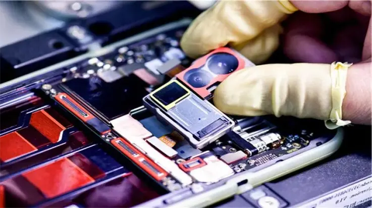
Ensuring Reliable Board-to-Board Connections in Phone PCBs
The connections between phone PCBs and other components, like modular boards or screen assemblies, need to be robust and reliable. To achieve this, it’s essential to focus on board-to-board connections. These connections ensure that the various parts of the smartphone work together seamlessly.
Connectors and flexible printed circuits (FPCs) are commonly used for these connections. The goal is to maintain a strong electrical connection that can handle the device’s high-speed data requirements while also ensuring physical durability, especially when subjected to regular handling or bending, as is often the case with foldable smartphones.
One emerging technology is the use of high-frequency connectors that can transmit high-speed signals between boards with minimal loss or interference. When it comes to 5G or performance-heavy devices, these connectors make sure the signal stays strong and clear, even under heavy usage. They’re the hidden heroes that keep data flowing with minimal lag, keeping your devices locked in and performing at their peak.
Board-to-Board Connection Examples-
| Connection Type | Application | Benefit |
| FPC Connectors | Used in flexible circuits for foldable smartphones | Flexible, lightweight, and durable connection |
| High-Frequency Connectors | Used for 5G signal transmission between boards | Reduces signal loss, enabling high-speed data |
| Standard Pin Header Connectors | Common for modular designs in smartphones | Provides a strong and reliable connection |
In Samsung’s Galaxy Fold, board-to-board connections are made possible with FPC connectors that allow the device to fold without interrupting data flow, ensuring continuous high-performance operation.
Inspection Standards for Assembled Mobile Phone PCBs
Once the assembly is complete, it’s time for inspection. Rigorous inspection standards are necessary to ensure that mobile phone PCBs meet all required functional and performance criteria before they are sent to the final product assembly.
A few of the most commonly used inspection techniques are:
●Automated Optical Inspection (AOI): This technique is used to check the surface of the assembled PCB for defects like misplaced components, short circuits, and soldering issues.
●X-Ray Inspection: For more complex, multi-layer boards, X-ray inspection is used to detect hidden defects like voids in solder joints or misaligned components that might not be visible on the surface.
●Electrical Testing: Electrical testing ensures that all the connections on the mobile phone PCB are intact and functioning as expected.
These inspection standards are designed to catch defects early and ensure that only the most reliable mobile phone PCBs make it into production.
Common Inspection Techniques and Their Benefits-
| Inspection Method | Purpose | Benefit |
| Automated Optical Inspection (AOI) | Surface-level defect detection, including misalignment of components | Ensures all components are correctly placed and soldered |
| X-ray Inspection | Detects defects in internal layers or hidden components | Prevents failure in multi-layer complex designs |
| Electrical Testing | Confirms proper connections and functionality | Ensures no faulty connections that could compromise device operation |
For Huawei, the use of X-ray inspection technology in their PCB assembly process ensures the internal components are correctly aligned and soldered, especially in complex multi-layer PCBs where errors could lead to device malfunction.
Future Innovations in Phone PCB and Mobile Phone PCB Design
The future of mobile phone PCB design is nothing short of exciting, with new technologies on the horizon that will drive the next generation of smartphones. From 5G to flexible designs, these innovations promise to revolutionize how mobile phone PCBs are built, improving both performance and user experience.
Meeting 5G Requirements in Mobile Phone PCBs
The demand for 5G connectivity has already started to reshape how mobile phone PCBs are designed. As the world transitions to 5G, mobile devices will need to handle faster speeds, more data, and better connectivity. This calls for PCB designs that can handle these increased demands without sacrificing performance.
To meet these requirements, mobile phone PCB designs need to be optimized for higher frequencies and lower signal loss. This means incorporating materials like high-frequency laminates and optimizing the PCB stack-up to reduce signal interference. 5G-compatible PCBs require tighter impedance control and better thermal management.
Key Components for 5G Mobile Phone PCBs-
| Component | Purpose | Benefit |
| High-Frequency Laminates | To support higher-frequency signals | Minimizes signal loss and interference |
| Optimized PCB Stack-up | Design layers for efficient signal transmission | Ensures consistent data flow at high speeds |
| Improved Thermal Management | Helps dissipate heat from high-speed components | Reduces overheating in 5G-enabled devices |
For example, Qualcomm’s Snapdragon 888 chipset, designed for 5G smartphones, integrates 5G antennas directly onto the PCB, showcasing how next-gen PCBs are adapting to emerging technologies.
System-in-Package (SiP) and Integration in Phone PCBs
One of the cutting-edge innovations in mobile phone PCB design is System-in-Package (SiP) technology. SiP allows multiple chips or components to be integrated into a single module, which reduces the size of the PCB while improving the performance and efficiency of the device.
SiP technology is especially useful for compact mobile devices that require small form factors but still need to house advanced components like processors, memory, and sensors. The integration of multiple components into a single package minimizes the number of interconnections, resulting in better signal integrity and reduced power consumption.
SiP Advantages and Application-
| Advantage | Impact | Application in Phone PCBs |
| Reduced Size | Allows for a more compact device design | Essential for slim smartphones |
| Enhanced Performance | Improves communication between components | Used in high-performance mobile devices |
| Lower Power Consumption | Minimizes energy use while maintaining performance | Perfect for battery-efficient designs |
Apple’s A-series chips are an excellent example of SiP technology. By integrating multiple processors, memory, and wireless components into a single package, Apple has been able to achieve powerful mobile devices in compact packages.
Advances in Flexible Mobile Phone PCB Applications
Flexible PCBs are transforming the mobile device industry by opening up new possibilities, including foldable smartphones and wearables. As mobile phone designs evolve to feature flexible and rollable displays, there’s an increasing demand for PCBs that can keep up with these dynamic shifts. The need for flexibility in design has pushed many circuit boards manufacturers to develop more adaptable, durable PCBs that can bend and twist without compromising performance. Simply put, the ability to innovate with these flexible boards is changing the way we think about device design.
The flexibility of these PCBs allows them to be bent and molded into various shapes, making them ideal for the next generation of smartphone designs. By incorporating flexible PCBs, Many manufacturers can produce lightweight, space-saving devices that still offer excellent performance.
In addition to foldable screens, flexible PCBs are used in wearables, smartwatches, and health monitoring devices where traditional rigid PCBs simply don’t fit. Conductive inks and advanced materials are used to create flexible circuits that maintain reliability, even in the most compact and dynamic environments.
Benefits of Flexible Mobile Phone PCBs-
| Feature | Benefit | Impact on Mobile Devices |
| Bendability | Allows for unique and compact designs | Essential for foldable and flexible phones |
| Lightweight | Reduces the overall weight of the device | Perfect for wearable tech and smartwatches |
| Durability | Stands up to wear and tear in daily use | Helps in creating long-lasting devices |
Samsung’s Galaxy Z Flip is a prime example of how flexible PCBs are pushing the boundaries of smartphone design, providing a high-performance device that’s both foldable and durable.
Flexible and Rigid-Flex Mobile Phone PCBs for Next-Gen Devices
In today’s mobile phone market, flexible and rigid-flex PCBs are becoming indispensable for designing next-gen devices. With smartphones, wearables, and foldable displays pushing the envelope of what’s possible in terms of form factor and performance, the demand for flexible phone PCBs is skyrocketing. These advanced technologies allow designers to create smaller, more compact devices without sacrificing durability or functionality.
Design Techniques for Foldable Mobile Phone PCBs
Designing foldable mobile phone PCBs is no small feat. When developing these devices, we need to address several unique challenges, including how to ensure reliability when the phone is repeatedly bent. The bending and folding action requires PCB designs that are both durable and flexible enough to withstand repeated use without compromising the performance of internal components.
One of the key design considerations for foldable PCBs is the use of flexible substrates. Materials such as polyimide film are commonly used for their ability to withstand bending without losing conductivity or signal integrity. Additionally, multi-layer flexible PCBs are designed with special materials that provide better mechanical stability during flexing. The integration of microvias and other advanced techniques enables smaller, more efficient designs that still meet performance standards.
Example: For a phone like the Samsung Galaxy Z Fold, the flexible PCB has to accommodate the bending mechanism without introducing any short circuits or signal loss. This is achieved through careful layer stacking and material choice, ensuring that the flexible design aligns with the device’s overall performance goals.
Key Design Considerations for Foldable Phone PCBs-
| Consideration | Solution | Benefit |
| Bending Resistance | Use of polyimide and other flexible materials | Enables foldable phones without performance degradation |
| Signal Integrity | Incorporating microvias and advanced materials | Maintains stable electrical connections despite bending |
| Component Miniaturization | Designing smaller, more efficient components | Reduces the overall footprint of the phone |
Reliability Testing for Flexible Phone PCBs
The durability of flexible PCBs is a major concern, particularly for foldable phones, which experience continuous bending and folding.To make sure these boards don’t fold under pressure, we put them through some serious stress tests. These tests mimic everything from daily bending to wild temperature changes and even moisture. It’s like giving them a workout at the gym, ensuring they stay tough and reliable long-term, no matter what gets thrown at them.
A common test for flexible phone PCBs is the flexural test, which bends the PCB to simulate real-life use. The goal is to assess whether the PCB can handle stress without cracking, delaminating, or losing electrical functionality. Along with mechanical testing, thermal cycling tests are also employed to simulate how the PCB will react to extreme temperature fluctuations that might occur during daily use.
Testing Methods for Flexible Phone PCBs-
| Test Type | Purpose | Outcome |
| Flexural Test | Simulates daily bending and folding of the device | Ensures the PCB remains intact after repeated bends |
| Thermal Cycling | Tests PCB performance under temperature fluctuations | Verifies stability in high and low-temperature conditions |
| Environmental Stress Test | Assesses PCB durability in varying humidity conditions | Confirms long-term reliability and resistance to corrosion |
By passing these tests, a flexible PCB can be certified as suitable for use in high-performance mobile devices like smartphones and wearables.
Advantages of Rigid-Flex PCBs in Compact Mobile Devices
Rigid-flex PCBs are a hybrid solution that combines the best features of both rigid PCBs and flexible PCBs. These boards have both rigid and flexible sections, allowing for a more compact and reliable design. Rigid-flex PCBs are ideal for compact mobile devices because they allow designers to pack more functionality into a smaller space, which is perfect for modern smartphones and wearable technology.
The primary advantage of rigid-flex PCBs lies in their space-saving nature. By incorporating both flexible and rigid components, we can eliminate the need for multiple interconnecting wires and connectors. This not only reduces the overall size but also enhances the reliability and performance of the device. Moreover, rigid-flex PCBs are often used in multi-functional devices like smartwatches and fitness trackers, where space is limited but performance cannot be compromised.
Benefits of Rigid-Flex PCBs in Mobile Devices-
| Benefit | Application | Impact |
| Space Efficiency | Smartphones, wearables | Reduces the overall size of the device |
| Improved Durability | Multi-function mobile devices | Offers increased resistance to bending and flexing |
| Enhanced Performance | High-performance consumer electronics | Minimizes signal loss and power consumption |
Apple’s Apple Watch uses rigid-flex PCB technology to maximize the use of limited space while maintaining a high level of reliability and performance. The rigid-flex design allows the board to curve around the device’s form factor while also maintaining rigid sections where traditional connections are necessary.
Your Leading Cell Phone PCB Supplier from China – JarnisTech!
Looking for top-quality mobile phone PCBs? Look no further! JarnisTech stands as one of the largest printed circuit board manufacturers in China, offering cutting-edge solutions for all your mobile phone PCB needs. With over 20 years of experience, we’ve become a trusted name in the industry, delivering innovative and reliable PCBs to companies around the globe.
At JarnisTech, we pride ourselves on our advanced manufacturing facilities, where we leverage the latest technology and materials to create high-performance PCBs that cater to your specific requirements. Whether you’re developing a new smartphone, designing a foldable device, or working on an innovative solar-powered phone charger, we have the capabilities to bring your vision to life.
1. High-Quality Materials for Superior Performance
Our cell phone PCBs are constructed from epoxy-fiberglass composite (FR-4), known for its non-conductive properties and superior electrical and mechanical performance. These durable materials ensure your PCBs stand the test of time, even in the most demanding applications. With multiple layers laminated together, our PCBs integrate components on both the top and bottom layers, enabling a higher density of circuits and more sophisticated designs.
2. Diverse Mobile Phone PCB Applications
As a leading manufacturer, we offer a broad range of mobile phone PCB solutions, including:
●Android Mobile Phone PCBs – Supporting Android devices with reliable, high-quality boards designed for everyday use.
●Mobile Phone Charger PCBs – Durable charging boards, optimized for both efficiency and safety.
●Solar Phone Charger PCBs – Powering devices with sustainable energy, ideal for eco-conscious users.
●Foldable Phone PCBs – With innovative designs for flexible and foldable phones, ensuring that advanced features work seamlessly.
3. Why Choose JarnisTech?
JarnisTech isn’t just another PCB manufacturer; we’re your partner in success. From initial cost calculations to production monitoring and quality control, we handle every aspect of the manufacturing process to ensure that you receive top-notch products at competitive prices.
| Service | Details | Benefit |
| Expert Manufacturing | State-of-the-art facilities and experienced team | Ensures precise and efficient PCB production |
| Global Reach | Supply to over 500 companies worldwide | Reliable and scalable PCB solutions |
| Quality Control | Strict quality standards at every production stage | Delivers consistent, high-performance products |
Proven Expertise and Reliability-
We’ve earned our reputation as a reliable PCB supplier by consistently delivering high-quality products that meet global standards. Whether you’re producing smartphones or creating innovative mobile accessories, you can trust JarnisTech to provide durable, efficient, and cost-effective solutions that exceed expectations.
Ready to make your next mobile phone design a success? Get in touch with us today and see how we can help streamline your PCB production and Assembly process!
FAQs about Phone PCBs
What is a Phone PCB?
A Phone PCB (Printed Circuit Board) is the central component that connects and supports all the electronic parts in a mobile phone, including processors, sensors, and memory.
What materials are used for Phone PCBs?
Most phone PCBs are made from FR-4 (epoxy fiberglass) due to its strong insulating properties and durability.
What types of Phone PCBs are there?
Common types include single-layer, double-layer, and multilayer PCBs, with HDI and rigid-flex options for advanced designs.
What is HDI in Phone PCB?
HDI (High-Density Interconnect) PCBs use microvias and small vias to support more complex designs, enabling smaller and more efficient circuits.
How are Phone PCBs manufactured?
Phone PCBs are produced using layered materials, precision etching techniques, and soldering processes to create circuits and connections.
What is the lifespan of a Phone PCB?
The lifespan varies, but with proper manufacturing and design, Phone PCBs can last many years, typically aligning with the phone’s overall durability.
What is the role of quality control in Phone PCB production?
Quality control ensures Phone PCBs meet strict standards for electrical performance, durability, and safety, reducing defects in the final product.


