
In today’s world of advanced PCB design and manufacturing, Via Filled and Via-in-Pad technologies have become central to creating high-performance circuit boards that meet the ever-growing demands of industries like electronics, automotive, and medical devices. These techniques, while complex, allow for innovative design approaches, enhanced signal integrity, and superior thermal performance in densely packed designs.
In this article, we will walk through these technologies step by step, explaining their applications, challenges, benefits, and the best practices to ensure they are used effectively. We’ll take a closer look at how these methods enable manufacturers to meet the increasingly sophisticated needs of modern PCBs.
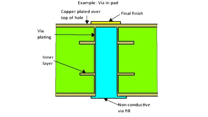
What is Via Filled Technology?
Via-filled technology involves filling the vias in a PCB with a material, typically copper or non-conductive epoxy, to enhance both the mechanical strength and electrical performance of the circuit. This technique has grown increasingly popular as the demand for miniaturized and high-density designs has risen. By filling the vias, the PCB can be made more robust and capable of handling higher electrical loads and thermal demands.
1.Definition and Significance in PCB Design
Via filling is the process of completely filling the hole, or via, with a specific material such as copper, epoxy, or non-conductive materials. The filled via eliminates the voids that can cause electrical performance degradation, thus improving the reliability and lifespan of the PCB. This method is often used in high-performance circuits where signal integrity and thermal management are non-negotiable.
2.Types of Via Filling Materials
●Copper-filled vias: These are the most commonly used type of via filling. They are essential when electrical conductivity between layers must be maintained without compromise. Copper-filled vias are ideal for high-frequency applications, as they minimize signal loss and reduce impedance mismatches.
●Epoxy-filled vias: This material is primarily used for non-conductive vias. It’s perfect for preventing cross-talk and short circuits, especially in designs that feature sensitive signal paths. Epoxy filling also enhances mechanical stability, making it ideal for flexible or rigid-flex PCBs.
●Non-conductive filled vias: These are commonly used in high-density designs, where certain vias must be insulated to prevent unwanted electrical conductivity. Non-conductive filled vias are often paired with specialized coatings to further improve the board’s thermal performance and durability.
If you’re looking for non-conductive epoxy to use to fill your via it is usually one of the Peters PP2795 epoxies. But, an alternative that has been popular in the past few times has been San-Ei-Kagaku PHP-900 epoxy. Both of them should be able to meet the basic requirements for an epoxy that is non-conductive.
3.Why Use Via Filling?
Via filling is often employed in designs that feature high-density interconnects (HDI), such as those found in smartphones, medical devices, and other compact consumer electronics. By filling the vias, the PCB achieves:
●Enhanced electrical performance: With no air gaps, signal loss and reflection are minimized.
●Improved mechanical stability: The filling process strengthens the board, making it more durable against thermal cycling and mechanical stress.
●Better thermal dissipation: Via filling helps in heat management, especially in high-power applications.
What is Via-in-Pad Technology?
On the flip side, via-in-pad technology involves placing the via directly in the pad area, which is typically where components like BGAs (Ball Grid Arrays) or other high-density packages are placed. This technique is often employed in the design of microvias and HDI PCBs, where space is at a premium. Let’s break down the specifics of this technique.
Role in Compact Designs with Microvias and BGA Layouts
Via-in-pad is particularly beneficial in compact designs, like those required for mobile devices, wearable technology, and medical electronics, where PCB space is scarce. By using microvias and placing vias directly under component pads, we can create a more compact, efficient, and space-saving layout. In short, Via-in-Pad makes it possible to push the boundaries of space-constrained technology while maintaining top-notch performance.
Benefits for Signal Performance and SMT Compatibility
Via-in-pad technology has a profound impact on signal integrity and SMT (Surface-Mount Technology) compatibility. By locating vias directly under the pads, you reduce the potential for signal loss and improve electrical performance, especially in high-speed designs. Additionally, this setup eliminates the need for external vias that could interfere with SMT assembly, which is an added benefit for automated assembly lines.
A classic example is the use of via-in-pad in high-performance BGA packages. The BGA’s balls or pads are placed directly over the vias, ensuring minimal signal degradation. By integrating via-in-pad, we can maximize performance in compact spaces without sacrificing speed or reliability, making it the go-to choice for next-gen tech that demands high performance in a small footprint.
Advantages of VIP Technology Over Blind Vias and Buried Vias
Via-in-Pad (VIP) technology has proven to be an advantageous choice when compared to traditional via technologies like blind vias and buried vias. Below, we will delve deeper into how VIP technology stacks up against these alternatives, highlighting the unique advantages it offers in high-performance, high-density designs.
1.Ideal for BGAs with Fine Pitch-
When dealing with Ball Grid Arrays (BGAs) with fine-pitch configurations, traditional vias can sometimes cause routing challenges. VIP technology, however, resolves these challenges by embedding the via directly into the pad, providing an efficient solution for connecting complex BGA pins.
●What’s the Big Deal?
For designs that require dense routing, VIP technology enables precise pad placement, reducing the chances of signal interference or connection problems. This technique is especially useful in devices that feature fine-pitch components like BGAs, commonly seen in smartphones, wearables, and high-end computing devices. With VIP, space is optimized, and signal paths are kept clean, allowing for strong and reliable connections even in compact, high-performance designs.
●Why VIP?
Fine-pitch BGAs demand a level of precision that VIP technology provides, leading to fewer routing constraints, even in highly congested areas of the PCB.
| BGA Pitch Size | Via-in-Pad Advantage | Traditional Via |
| 0.5 mm | No interference, accurate signal routing | May require more routing space, causing potential layout inefficiencies |
| 0.3 mm | Seamless pad integration, optimal for high-density layouts | Less suitable for fine-pitch designs due to size limitations |
2.Increasing PCB Density and Saving Space-
As electronics shrink in size, the demand for high-density interconnects increases. VIP technology is particularly beneficial for maximizing space on a PCB. By integrating vias into the pads, VIP eliminates the need for dedicated trace routing around each via, making it possible to fit more components into a smaller area.
●Space-Saving Design: VIP technology minimizes the amount of required surface area for vias, allowing PCB designers to add more components or features while maintaining the integrity of the design.
●What’s the Outcome?
The result? More efficient layouts with denser routing and smaller PCB footprints, ensuring that designs meet ever-shrinking space requirements in consumer electronics, automotive, and industrial devices.
| Design Objective | Via-in-Pad Technology | Blind/Buried Vias |
| PCB Real Estate | Smaller footprint, increased density | Occupy more surface area, limited routing flexibility |
| Performance Impact | Optimized for high-density, high-performance designs | Limited by routing space and internal layer connectivity |
3.Enhanced Thermal Performance-
VIP technology not only improves routing efficiency but also plays a significant role in thermal management. With the growing demand for higher power densities, especially in components like power ICs, effective heat dissipation is a top priority.
●Heat Dissipation Advantage: By placing vias directly in the pads, VIP technology helps to spread heat more evenly across the board, allowing thermal vias to directly channel heat away from sensitive components. This is especially beneficial for high-power electronics and automotive applications where heat management is a priority.
●How Does It Work?
When copper-filled vias are used, the via in pad technology can enhance thermal conductivity, reducing the risk of hot spots and improving overall system reliability. This approach is particularly effective in applications like LED lighting, automotive electronics, and RF modules.
| Thermal Management | Via-in-Pad Technology | Blind/Buried Vias |
| Heat Dissipation | Direct heat conduction via copper-filled vias | Less efficient heat flow, not directly addressing thermal hotspots |
| Power Electronics & LEDs | Enhanced cooling in high-power applications | Limited by surface area for heat dissipation |
4.Minimizing Inductance in High-Speed Designs-
High-speed designs demand minimal signal distortion, and one of the critical factors that can affect this is inductance. VIP technology mitigates this issue by shortening the signal path and reducing the distance between components.
●Inductance Reduction: With traditional vias, signal paths can become longer and more prone to signal loss and crosstalk. VIP allows for more direct routing, optimizing the signal path and enhancing signal integrity in high-speed circuits, such as those used in 5G technology or high-performance computing.
●What’s the Result? By utilizing VIP technology, designers can achieve low-inductance, high-speed interconnects, making it easier to manage high-frequency signals without interference or loss of data integrity.
| Signal Integrity | Via-in-Pad Technology | Blind/Buried Vias |
| Inductance | Shorter signal paths, minimal distortion | Longer traces may introduce signal integrity issues |
| High-Speed Performance | Optimal for high-frequency signals | Less efficient at higher speeds, with potential for delays |
5.Flat Surface for Component Attachment-
One of the standout advantages of via-in-pad technology is its flat surface, making it ideal for surface mount technology (SMT). This flat surface ensures uniform soldering and easy attachment of components.
●Simplified SMT Assembly: The even surface, with vias embedded directly in the pad, eliminates the risk of solder wicking, where solder flows down the vias during assembly, potentially disrupting the connection. It provides stronger, more reliable joints.
●Increased Manufacturing Efficiency: VIP technology allows for faster, more consistent manufacturing processes, ensuring that high-quality connections are achieved for even the most sensitive components.
| Component Mounting | Via-in-Pad Technology | Blind/Buried Vias |
| Surface Mount Technology | Flat surface for easy attachment | Surface irregularities may cause assembly issues |
| Soldering Reliability | Consistent solder joints, reduced risk of wicking | Risk of poor soldering due to via exposure |
6.Efficient Routing-
Finally, VIP technology allows for smarter routing. By embedding vias in the pads, we can eliminate redundant routing and use the same layer for both component attachment and via placement, saving both space and time.
●Efficient Routing: With fewer layers and minimized need for trace routing around vias, PCB layouts become simpler, enabling quicker designs and faster manufacturing cycles.
●Reduced Trace Length: Shorter traces lead to fewer opportunities for signal degradation, making VIP ideal for high-speed signal routing applications.
| Design Efficiency | Via-in-Pad Technology | Blind/Buried Vias |
| Layout Optimization | Saves space and simplifies design | Requires more routing space, adding complexity |
| Routing Complexity | Shorter, more direct traces | Longer traces may increase complexity |
Key Differences Between Via Filled and Via-in-Pad
While both via-filled and via-in-pad technologies serve the purpose of improving PCB performance, their applications and implementation are quite different. Here’s how they stack up:
1.Structural Differences
The most noticeable difference is in how the vias are treated. In via-filled technology, the via is completely filled with material, whereas in via-in-pad, the via is placed directly under the pad of the component, typically a BGA or QFN (Quad Flat No-lead) package. Via-in-pad is often used for high-density components that require precise routing paths, whereas via filling is used to enhance the overall structural integrity and electrical performance of the PCB.
2.Application Scenarios for HDI and Advanced PCBs
●Via-filled technology is frequently applied in high-density interconnects, flexible PCBs, and rigid-flex designs, where precise connections and performance are needed. This approach is commonly used in sectors like medical devices, military electronics, and automotive systems, where dependable and high-performing circuit boards are required. It helps improve signal integrity and offers better thermal management, making it suitable for applications that demand strong, consistent performance under challenging conditions.
●Via-in-pad technology finds its place in designs that demand extreme miniaturization, such as smartphones, tablets, laptops, and other compact electronics. When combined with microvias, this technique allows for precise routing in high-density layouts where space is limited. By placing vias directly under the component pads, we can maximize the PCB’s functionality while minimizing its footprint. This method proves particularly useful in applications where traditional routing strategies won’t meet the size and performance requirements, making it a go-to solution for high-performance, space-constrained circuits.
| Feature | Via Filled | Via in Pad |
| Material Used | Copper, epoxy, non-conductive materials | Copper, typically with non-conductive coating |
| Application | High-performance, high-density designs | Space-saving, microvia, and BGA integration |
| Purpose | Improve signal integrity, thermal dissipation | Ensure pad integrity and optimize layout for BGAs |
| Common Use Cases | Medical, aerospace, automotive, high-speed PCs | Mobile devices, consumer electronics, IoT |
| Primary Benefit | Enhanced electrical and mechanical stability | Optimized for compact designs and SMT |
Advantages of Using Via Filled and Via-in-Pad in PCB Manufacturing
Via-filled and via-in-pad technologies have proven to be essential tools for addressing several challenges in modern PCB manufacturing, especially when it comes to signal integrity, thermal management, and miniaturization. Let’s break down the real-world advantages of using these techniques in your designs.
Enhancing Signal Integrity with Via-in-Pad
In high-speed designs, signal integrity is everything. Via-in-pad technology ensures that the signals running through your PCB are delivered clean and without distortion—an absolute must in devices like smartphones and automotive electronics where every millisecond counts.
1.Minimizing Signal Distortion-
One of the main challenges in high-frequency designs is maintaining a steady signal without degradation. Vias, when placed incorrectly, can create unwanted resistance and signal loss. Via-in-pad addresses this issue by strategically placing the via directly beneath component pads, which minimizes the path for the signal to travel, reducing the chances for distortion or loss. This placement is particularly useful for BGAs (Ball Grid Arrays), where traditional via placements can lead to poor electrical performance.
Example: In a 5G module, signal distortion could lead to latency issues or even connection dropouts. By utilizing via-in-pad, manufacturers can maintain the integrity of high-speed signals, ensuring reliable, high-bandwidth transmission across the board.
2.Avoiding Interference-
When multiple layers of a PCB are stacked on top of one another, managing interference becomes a real challenge. Vias that aren’t properly optimized for signal routing can contribute to electromagnetic interference (EMI). Via-in-pad not only helps reduce this interference but also allows engineers to design with more flexibility, ensuring that vias don’t interrupt the path of sensitive signals.
Tip: To get the most out of via-in-pad technology, ensure that vias are properly plated and that the pads are well-aligned to avoid mechanical stresses, which could lead to yield issues during manufacturing.
3.Signal Integrity Comparison-
| Via Type | Signal Distortion | Resistance (Ohms) | Impact on High-Speed Signals |
| Standard Via | High | 0.25-0.5 | Can cause significant signal loss at high frequencies. |
| Via-in-Pad | Low | 0.05-0.1 | Minimizes signal loss and reduces distortion, enhancing signal clarity. |
Key Takeaway: Via-in-pad technology minimizes signal distortion by reducing the signal path length and improving signal quality at high frequencies.
Improving Thermal Dissipation with Via Filled Technology
When designing PCBs for heat-sensitive components, like those in power electronics or automotive systems, managing heat dissipation is a major focus. Via-filled technology helps keep components from overheating, which could otherwise lead to malfunctions or even serious safety risks. By effectively channeling heat away, this approach ensures the reliability and longevity of your devices, especially in environments where performance demands are high.
1.Role of Thermal Vias in Heat-Sensitive Components-
In many designs, particularly those that involve high-current or high-voltage systems, thermal vias are used to conduct heat away from sensitive areas, ensuring components remain within safe temperature limits. Via-filled technology enhances this process by filling vias with materials that offer better heat conductivity than standard PCB materials. Copper-filled vias, for example, can act as excellent heat sinks, directing heat away from critical areas and improving overall thermal performance.
Application: In electric vehicles (EVs), power modules often need to handle intense heat. By utilizing via-filled copper in areas where the heat is most concentrated, we can ensure that these power modules stay within safe operating temperatures, extending the life of the components and boosting overall system efficiency.
2.Application in Power Electronics and Automotive Systems-
Power electronics and automotive circuits often handle both high power and high heat, so our PCB designers need to come up with solutions that manage heat without affecting the circuit’s functionality. Via-filled technology is a great fit for these applications, especially in multi-layer PCBs. In these designs, thermal vias help distribute heat evenly across multiple layers. When filled with copper, these vias offer excellent heat transfer, keeping components like power transistors or motor controllers from overheating.
Example: In an electric car’s power supply unit (PSU), via-filled technology helps keep the unit from overheating. By filling vias with a conductive material, we channel the heat away from high-power components. This setup keeps the heat from spreading to nearby parts, preventing potential issues like thermal runaway and ensuring that the system stays stable.
3.Thermal Dissipation Efficiency-
| Via Type | Thermal Conductivity (W/m·K) | Application Areas | Efficiency |
| Standard Thermal Via | 200 | Used for moderate heat dissipation in general electronics. | Good for small power applications. |
| Copper-Filled Via | 390 | Ideal for power electronics, automotive circuits, and high-frequency devices. | Great for high-power components and efficient thermal management. |
Key Takeaway: Copper-filled vias significantly improve thermal dissipation, making them ideal for power electronics and high-heat applications like electric vehicles.
Enabling Miniaturization and High Routing Density
As consumer electronics continue to get smaller and more powerful, miniaturization becomes a must. This is where via-in-pad and via-filled technologies step in. These techniques let us push the boundaries of PCB design by allowing for denser routing and more compact layouts, all while keeping performance and reliability on point. These methods help us pack more power into a smaller space, delivering top-tier results without compromise.
1.Importance for HDI Boards and Multi-layer PCBs-
High-Density Interconnect boards, which are commonly used in smartphones, wearables, and medical devices, require extremely compact designs. Traditional designs with large vias and traces simply won’t cut it when you need to pack more functionality into less space. Via-in-pad and via-filled techniques help make this happen by offering smaller vias that don’t require the large copper pads that would traditionally take up precious space on the board. These designs can now include more routing paths, making it possible to fit more complex circuitry into a smaller form factor.
2.Case Studies on Achieving Compact PCB Designs-
Take the example of a smartphone motherboard. Modern phones are packed with features—cameras, processors, wireless modules—yet they still manage to stay slim. This is made possible by via-in-pad technology, which allows us to route signals underneath components without compromising space. By using this technique,we are able to achieve higher routing densities, reducing the overall size of the PCB while increasing its functionality.
Example: In a smartphone, the small size and high demand for performance often require using via-in-pad for placing high-speed connections underneath the BGA and other chip components. With this approach, we can achieve high-density routing without the need for large, space-consuming traces, allowing the phone to stay sleek and functional.
3.HDI Board Comparison-
| Technology | Routing Density | Size Reduction | Common Use Cases |
| Traditional Vias | Low | Limited | Suitable for larger, less complex designs. |
| Via-in-Pad | High | Significant | Used for compact, high-performance designs like smartphones and medical devices. |
Materials Used in Via Filled and Via-in-Pad Technologies
The materials used in via-filled and via-in-pad technologies play a central role in determining the performance and reliability of the final PCB. Each material type is chosen based on the application’s specific requirements, including thermal management, mechanical stability, and cost-efficiency. Whether you’re designing for aerospace systems, medical devices, or consumer electronics, understanding these materials’ properties and use cases will help you make informed decisions.
Below, we’ll break down the most common materials used in these technologies, discuss their applications, and compare their performance. Let’s dive in!
Copper-Filled Vias
Copper-filled vias are widely used in PCB manufacturing, thanks to their excellent thermal and electrical conductivity. Copper not only provides a robust pathway for heat dissipation but also enhances the mechanical stability of the vias, making them suitable for high-reliability applications.
1.Advantages of Copper-Filled Vias-
●Thermal Management: Copper is a great conductor of heat, with a thermal conductivity of approximately 390 W/m·K, making it ideal for applications that generate significant heat, such as power electronics or LED circuits.
●Mechanical Strength: The rigidity of copper-filled vias improves the board’s structural integrity, reducing the risk of delamination or cracking under mechanical stress.
●Electromagnetic Shielding: Copper also offers superior shielding for minimizing electromagnetic interference (EMI), making it indispensable in aerospace systems and medical devices.
| Parameter | Copper-Filled Vias | Impact |
| Thermal Conductivity | 390 W/m·K | Excellent for heat-sensitive designs |
| Mechanical Strength | High | Reduced risk of cracking or delamination |
| Cost | High | Suitable for high-performance PCBs |
Epoxy-Filled Vias
Epoxy, a non-conductive material, provides an affordable alternative to copper for via filling. While it doesn’t have the same thermal conductivity as copper, epoxy-filled vias are commonly used in HDI PCB production, where low cost and lightweight designs are top priorities. However, achieving solid adhesion and reliable solderability with epoxy can still present challenges.
1.Benefits of Epoxy-Filled Vias-
●Cost Efficiency: Epoxy is significantly more affordable than copper, making it a popular choice for consumer electronics and mid-range applications.
●Lightweight: Epoxy is ideal for designs where reducing the board’s overall weight is important, such as in wearable devices or portable medical equipment.
2.Challenges to Consider-
●Solderability: Improper curing of epoxy can lead to voids or weak solder joints, which can compromise reliability.
●Thermal Limitations: With a thermal conductivity of around 0.2 W/m·K, epoxy does not perform well in high-heat applications.
| Parameter | Epoxy-Filled Vias | Impact |
| Thermal Conductivity | ~0.2 W/m·K | Limited heat dissipation |
| Cost | Low | Affordable for budget-conscious designs |
| Solderability | Moderate | Requires careful processing |
Non-Conductive Filling Materials
Non-conductive filling materials, such as resin or epoxy variants, are commonly used for blind vias and buried vias in multi-layer PCB designs. These materials are chosen for their ability to maintain structural integrity without adding unnecessary weight or cost.
1.Applications of Non-Conductive Fillers-
●Blind Vias: These are vias that connect outer layers to inner layers without passing through the entire board. Non-conductive fillers prevent solder from flowing into these vias during reflow soldering.
●Buried Vias: Used in HDI PCBs, buried vias are completely encapsulated within the board, requiring filling materials that ensure long-term reliability under thermal cycling.
2.Comparison with Copper-Filled Vias-
While copper-filled vias excel in thermal and electrical conductivity, non-conductive materials are better suited for boards where cost and weight are more significant concerns. For example, in consumer electronics, non-conductive fillers offer a balance between performance and affordability.
| Parameter | Non-Conductive Fillers | Impact |
| Thermal Conductivity | Very Low (~0.2 W/m·K) | Not suitable for heat dissipation |
| Application | Blind and buried vias | Ideal for HDI boards |
| Cost | Moderate | Balanced for consumer electronics |
Manufacturing Processes for Via Filled and Via-in-Pad
The process of creating via-filled and via-in-pad PCBs demands precise attention to detail and strict adherence to manufacturing standards. It’s not simply about filling holes; this technique ensures that the PCBs are both reliable and perform at their best, particularly in HDI designs and cutting-edge applications.
Below, we outline the key manufacturing processes, potential challenges, and how to overcome them, supported by real-world examples and practical insights.
Steps in Copper Filling
Copper filling is an advanced method to fill vias, providing excellent thermal and electrical properties for demanding applications such as automotive electronics and aerospace systems.
1.Process Overview-
●Drilling and Cleaning: The first step involves drilling precise via holes, followed by cleaning to remove debris and contaminants that could compromise adhesion.
●Electroplating: A layer of copper is deposited inside the via using an electroplating process. Specialized plating baths are used to ensure uniform copper distribution across all vias, regardless of their size.
●Via Plugging: Copper paste or a similar conductive material is injected into the vias, followed by curing. This step eliminates voids and ensures that the vias can handle high currents and dissipate heat efficiently.
●Finishing: After curing, the board undergoes planarization to remove excess copper and ensure a smooth surface for subsequent layers.
2.Challenges and Solutions-
●Void Formation: Air pockets trapped during plating or plugging can lead to voids, which compromise electrical performance. Using vacuum-assisted filling systems significantly reduces void formation.
●Consistency in Microvias: For microvias, achieving uniform copper thickness is challenging. Optimized plating parameters and high-quality plating solutions address this issue effectively.
3.Example Use Case-
●In a 5G base station PCB, where high-speed signals demand superior thermal and electrical performance, copper-filled vias ensure minimal signal loss and efficient heat dissipation.
| Step | Objective | Key Equipment |
| Drilling and Cleaning | Prepares vias for uniform copper adhesion | Laser or mechanical drills |
| Electroplating | Deposits conductive copper layer | Plating baths with additives |
| Plugging | Ensures thermal and mechanical integrity | Vacuum via-fill systems |
Epoxy Filling Process
Epoxy filling offers a cost-effective alternative for via-filled applications, particularly in consumer electronics and low to mid-range HDI PCBs. While it doesn’t match copper in conductivity, epoxy excels in providing mechanical support and solderability.
1.Process Overview-
●Material Preparation: High-quality epoxy is mixed with additives to achieve the desired viscosity and thermal properties.
●Filling the Vias: Epoxy is injected under pressure to ensure complete filling. For microvias, automated systems are used to avoid incomplete fills.
●Curing: The board is subjected to controlled heating to cure the epoxy, solidifying its structure and ensuring long-term reliability.
●Surface Finishing: After curing, the excess epoxy is removed, and the surface is polished for smooth layering in subsequent steps.
2.Challenges and Solutions-
●Uniformity Issues: Uneven filling can lead to reliability issues. Advanced filling systems with real-time monitoring ensure consistent results.
●Solderability: Cured epoxy can sometimes interfere with solder adhesion. Using low-shrinkage, high-adhesion formulations helps address this.
3.Example Use Case-
In a smartwatch PCB, where compactness and cost control are key, epoxy-filled vias provide adequate mechanical support without inflating production costs.
| Step | Objective | Key Equipment |
| Material Preparation | Ensures viscosity and flow control | Epoxy mixers and dispensers |
| Filling | Prevents voids in blind and buried vias | Pressure-fill systems |
| Curing | Solidifies epoxy for durability | Controlled curing ovens |
Process Challenges and Solutions
Even the most advanced manufacturing processes are not without hiccups. Below, we explore common challenges faced in via filling and how we overcome them:
●Solder Wicking: In some cases, solder can flow into vias during assembly, causing connectivity issues. This is mitigated by using filled vias or applying solder mask over the vias.
●Misalignment: Misaligned vias can disrupt the entire PCB layout. Precision drilling and automated optical inspection (AOI) systems help maintain alignment.
●Thermal Expansion Mismatches: During thermal cycling, differences in expansion rates between the filler material and PCB layers can lead to cracks. Choosing materials with compatible coefficients of thermal expansion (CTE) is crucial.
| Challenge | Impact | Solution |
| Solder Wicking | Loss of electrical connectivity | Use filled vias or solder mask |
| Misalignment | Disrupted signal paths | Precision drilling and AOI |
| Thermal Mismatch | Cracks during thermal cycling | Use materials with matched CTE |
Design Challenges and Best Practices for Via-in-Pad and Via Filled
Designing printed circuit boards (PCBs) with via-in-pad and via-filled technologies demands a thorough understanding of their unique challenges and the adoption of advanced design practices. These approaches ensure optimized functionality, manufacturability, and cost-effectiveness, particularly in high-density, high-speed applications.
Addressing Solder Wicking Issues
Solder wicking occurs when solder flows into vias during surface mount technology (SMT) assembly, potentially leading to insufficient solder joints and defective connections. This issue becomes more pronounced in via-in-pad designs, where vias are placed directly under components like ball grid arrays (BGAs).
1.Strategies to Mitigate Solder Wicking-
●Filled and Capped Vias: Plugging vias with conductive or non-conductive materials and applying a copper cap prevents solder from seeping into the vias.
●Solder Mask Application: A carefully applied solder mask around the vias acts as a barrier, keeping the solder localized to the pad.
●Optimized Via Dimensions: Reducing the diameter of vias in sensitive areas minimizes solder wicking while maintaining mechanical and electrical reliability.
2.Best Practices for Reliable SMT Assembly-
●Ensure vias are thoroughly cleaned and filled to avoid solder voids.
●Utilize controlled reflow profiles to achieve consistent soldering.
| Method | Advantages | Challenges |
| Filled and Capped Vias | Prevents solder loss; reliable joints | Increases manufacturing complexity |
| Solder Mask Application | Simple and effective solution | Requires precise application |
| Optimized Via Dimensions | Reduces solder volume requirements | Limited by PCB design constraints |
Optimizing Layout for Signal Integrity
In high-speed PCB designs, keeping signal integrity in check is a must. Even the smallest disruptions in the signal path can lead to major performance issues. Where and how vias are placed can make or break a design, affecting everything from impedance control to signal delay and reducing the chances of unwanted cross-talk.
1.Best Practices for Via Placement-
●Strategic Via Spacing: Place vias at adequate distances to prevent overlapping electromagnetic fields, reducing interference and signal degradation.
●Via Stub Elimination: Utilize back-drilled vias to remove unnecessary via stubs, which can act as reflective surfaces and impair signal clarity.
●Microvia Utilization: Choose for microvias to shorten signal paths and minimize inductance, ensuring cleaner and faster signal transmission.
2.Reducing Cross-Talk-
●Ensure differential pair vias are symmetrically placed for balanced signal transmission.
●Use ground vias strategically to shield high-speed signals and dampen noise.
3.Performance Enhancement Guidelines-
●Implement controlled impedance for high-frequency traces.
●Conduct pre-layout simulation to identify and mitigate potential signal integrity issues.
| Technique | Benefit | Application Area |
| Back-Drilled Vias | Minimizes reflections and stub effects | High-speed digital circuits |
| Microvias | Shortens signal path for reduced loss | High-density interconnects |
| Ground Via Shielding | Dampens interference | Sensitive analog/digital interfaces |
Balancing Cost and Performance
Striking the right balance between cost efficiency and high performance requires careful consideration of materials, processes, and design choices. While advanced techniques like copper-filled vias offer superior electrical and thermal properties, they may not always be economically feasible for all applications.
1.Cost-Effective Alternatives-
●Epoxy-Filled Vias: These are less expensive than copper-filled options and suitable for low-power applications.
●Non-Conductive Fillers: Effective for mechanical support in non-critical applications, offering a balance of cost and reliability.
2.Material Selection Trade-offs-
●High-Performance Designs: Utilize premium materials like copper-filled vias for applications requiring exceptional thermal and electrical performance.
●Budget-Conscious Designs: For less demanding circuits, epoxy or non-conductive fillers provide adequate functionality without overshooting costs.
| Design Approach | Benefit | Limitation |
| Copper-Filled Vias | High thermal and electrical efficiency | Higher manufacturing cost |
| Epoxy-Filled Vias | Cost-effective for HDI boards | Limited thermal conductivity |
| Non-Conductive Fillers | Budget-friendly | Lower mechanical strength |
3.Guidelines for Balancing Costs-
●Prioritize performance-critical areas for premium solutions like copper-filled vias.
●Combine advanced and cost-effective materials within a single design to optimize resources.
When to Use Via Filled and Via-in-Pad in PCB Design?
Selecting between via filled and via-in-pad technologies hinges on the specific requirements of your PCB design, including performance, space constraints, thermal management, and cost considerations. These technologies are designed to address the demands of modern electronics, especially in high-density interconnects (HDI) and high-performance applications.
When to Choose Via Filled Technology?
Via filled technology is employed in scenarios where durability, thermal management, and electrical performance are key. This method involves filling vias with materials like copper, epoxy, or non-conductive resins, depending on the application.
Applications of Via Filled Technology-
1.Thermal Management:In power electronics or automotive systems, copper-filled vias are used to conduct heat away from components efficiently. For example:
●Power amplifiers in RF systems.
●High-current pathways in electric vehicle control boards.
2.Layer Interconnection: Via filled ensures robust electrical connections between multiple layers in HDI PCBs or multi-layer boards.
3.Mechanical Support: Provides enhanced structural stability for PCBs used in aerospace and medical devices, where reliability is non-negotiable.
| Scenario | Material | Advantages | Challenges |
| High heat dissipation | Copper-filled vias | Superior thermal conductivity | Higher manufacturing costs |
| Budget-sensitive designs | Epoxy-filled vias | Cost-effective and durable | Limited thermal performance |
| Mechanical reinforcement | Non-conductive fillers | Improves board stability | Reduced electrical conductivity |
When to Choose Via-in-Pad Technology?
Via-in-pad technology is favored for compact and high-speed designs where space constraints and signal integrity are top priorities. By embedding vias directly within component pads, we achieve shorter signal paths and enhanced routing density.
1.Applications of Via-in-Pad Technology-
●High-Density Designs: Commonly used in BGA layouts and microvias, where space is at a premium. This approach is indispensable for wearable devices, mobile phones, and IoT sensors.
●High-Frequency Circuits: Via-in-pad reduces signal distortion and ensures minimal impedance mismatch, making it ideal for 5G antennas and high-speed digital applications.
●Surface Mount Technology (SMT) Compatibility: Enables efficient soldering and alignment of components during assembly, ensuring high-quality connections.
| Use Case | Advantages | Considerations |
| Compact BGA packages | Reduces space consumption | Requires precise manufacturing |
| High-speed signal routing | Minimizes signal loss and distortion | May increase cost due to precision |
| Microvia designs | Enhances layer connectivity | Demands advanced fabrication tech |
Guidelines for Decision-Making
To determine whether to use via filled or via-in-pad technology, consider the following factors:
1.Performance Requirements: High-speed or high-frequency designs benefit from via-in-pad due to their superior signal integrity. Conversely, thermal-critical applications call for copper-filled vias.
2.Space Constraints:If space is tight and routing density needs to be maximized, via-in-pad is the go-to choice.
3.Budget and Fabrication Capability:While via filled can provide cost-effective solutions with epoxy or non-conductive fillers, via-in-pad may require advanced manufacturing capabilities, potentially increasing costs.
| Factors | Via Filled | Via-in-Pad |
| Heat dissipation | Excellent (Copper-filled) | Limited |
| Signal integrity | Moderate | High |
| Routing density | Moderate | Excellent |
| Manufacturing complexity | Moderate | High |
| Budget sensitivity | Suitable for low-cost applications | Typically higher cost |
Quality Control and Inspection Techniques for Via Filled and Via-in-Pad Technologies
Achieving robust and reliable PCBs hinges not only on design and manufacturing but also on the rigorous quality control processes that follow. For via filled and via-in-pad technologies, quality inspection ensures that these high-precision designs deliver exceptional performance across diverse applications. From uncovering hidden flaws to meeting industry certifications, meticulous testing safeguards your PCB’s journey from the lab bench to the field.
Leveraging X-Ray Inspection for Precision
X-ray inspection provides a powerful method for revealing hidden defects in vias and pads. This non-invasive technique allows for a detailed view into PCB layers, helping to identify issues like voids, misalignments, and incomplete fillings—concerns that could silently undermine your design’s reliability.
1.Key Applications-
●BGA Layout Verification: Detects misaligned vias beneath ball grid arrays (BGAs), ensuring proper signal connections and preventing costly failures during assembly.
●Void Detection in Via Filled Technology: Copper-filled vias must be void-free for optimal conductivity and thermal performance. X-ray inspection ensures the quality of each filled via.
| Inspection Parameter | Issue Detected | Impact on Performance | Solution |
| Void size and location | Thermal/electrical issues | Reduced heat dissipation and signal quality | Adjust filling/plating process |
| Misalignment in vias | Signal path disruption | Risk of circuit failure | Realign vias with drilling |
| Uneven copper plating | Impedance issues | Deteriorates high-speed performance | Adjust plating parameters |
Solderability Testing for Long-Lasting Performance
Solderability testing evaluates the PCB’s readiness for surface mount technology (SMT) processes. This is especially critical for via-in-pad designs, where solder wicking or uneven adhesion can wreak havoc during assembly.
1.Testing Techniques-
●Solder Paste Adhesion Testing: Ensures uniform application of solder paste, particularly around filled vias and pads. Irregularities can result in weak joints or voids beneath components.
●Reflow Simulation: Mimics real-world soldering conditions to test the interaction between vias, pads, and solder paste under high heat.
| Solderability Concern | Effect on PCB | Testing Method | Preventative Action |
| Uneven solder paste adhesion | Poor connection strength | Adhesion force testing | Optimize paste application process |
| Solder wicking into vias | Pad surface inconsistency | Cross-section microanalysis | Employ solder mask or via plugging |
| Voids in solder joints | Component instability | X-ray solder joint analysis | Adjust solder reflow profiles |
Reliability Testing for Extreme Conditions
In industries like automotive, aerospace, and industrial electronics, PCBs must endure harsh environments. Reliability testing simulates thermal cycling, mechanical stress, and vibration to ensure that via filled and via-in-pad technologies meet stringent durability standards.
1.Critical Testing Protocols-
●Thermal Cycling: Tests the PCB’s ability to withstand repeated temperature fluctuations, a common scenario in power electronics. Filled vias help distribute heat evenly, reducing stress-induced failures.
●Mechanical Stress Testing: Evaluates how vias and pads withstand stress, vibration, and physical deformation—particularly for PCBs used in high-impact fields such as automotive systems, where durability is put to the test.
| Test Type | Condition Simulated | Performance Metric | Benefits of Via Technologies |
| Thermal cycling | -55°C to 125°C for 1,000 cycles | Resistance to cracking/delamination | Via filled aids in thermal uniformity |
| Vibration testing | Frequency range 10-2,000 Hz | Structural integrity of via-in-pad | Enhanced mechanical stability |
| Moisture exposure | High humidity environments | Prevention of delamination | Epoxy-filled vias resist moisture |
Why Choose Us as Your PCB Manufacturer and Supplier?
In precision manufacturing, choosing the right PCB manufacturer ensures high-quality, reliable, and efficient designs. At JarnisTech, we take extra steps to offer tailored solutions for your PCB needs, including via-in-pad technology and via fill options. With years of experience in the field, we are well-equipped to handle complex PCB projects that demand high-performance and inventive solutions.
Our PCB Manufacturing Capabilities for Via Filled & Via in Pad:
| Capability | Via Filled | Via in Pad |
| Aspect Ratio | 12:1 (through-hole), 1:1 (blind/buried) | 1:1 (for high-density designs) |
| Via Diameter | 0.1mm – 0.8mm | 0.1mm – 0.6mm |
| Fill Type | Conductive (Copper), Non-Conductive (Epoxy) | Non-Conductive (Epoxy) |
| Via Type | Through-hole, Blind, Buried | Via-in-Pad (blind and buried) |
| Thermal Management | High thermal conductivity | Primarily mechanical |
| Soldering Compatibility | Reliable soldering, low voids | Requires precise filling to avoid defects |
| Drilling Precision | ±0.01mm | ±0.01mm |
| Layer Support | 4-46 layers | 2-46 layers |
| Material Used | Copper, Epoxy, Resin | Epoxy, Resin |
| Quality Control | X-ray for voids, plating control | Automated inspection for uniformity |
| Production Lead Time | 10-14 days (standard) | 12-16 days (standard) |
Ready to Take the Next Step?
At JarnisTech, we combine innovative technology, precision manufacturing, and expertise to deliver reliable, high-performance PCBs. Whether you’re working with via-in-pad or via fill technology, we’re ready to help you make the best choices for your design.
Get in touch with us today to start your journey toward the best possible PCB solution. Our team is excited to work with you and help you bring your vision to life!
FAQs related to Via Filled and Via-in-Pad
How does Via Filling help with thermal management?
Via Filled technology enhances heat dissipation by using thermal vias that effectively transfer heat from heat-sensitive areas to other parts of the PCB.
Can Via-in-Pad improve signal integrity?
Yes, Via-in-Pad minimizes signal distortion by reducing the inductance and improving the signal path for high-speed designs.
What materials are used for Via Fill?
Via Filled vias typically use copper or non-conductive materials like epoxy, while Via-in-Pad uses non-conductive epoxy or resin to ensure reliability and electrical isolation.
How does Via-in-Pad affect PCB manufacturing?
Via-in-Pad can complicate the manufacturing process, requiring precise alignment and special fill techniques, but it allows for smaller footprints and higher routing density.
What are the common challenges in Via-in-Pad technology?
Via-in-Pad can face issues like solder wicking or poor soldering, requiring additional quality control measures, including X-ray inspection.
Are there cost differences between Via Filled and Via-in-Pad?
Via-in-Pad tends to be more expensive due to the complexity of the process and the need for higher precision, while Via Filled is generally more cost-effective for standard designs.
Related Posts:
1. Important of Capped Vias Technology in PCB Design and Manufacturing


